Article

GaN-Based DC-DC Resonant Boost Converter with Very High Efficiency and Voltage Gain Control

Department of Power Electronics and Energy Control Systems, Faculty of Electrical Engineering, Automatics, Computer Science and Biomedical Engineering, AGH University of Science and Technology, al. Mickiewicza 30, 30-059 Krakow, Poland
*
Author to whom correspondence should be addressed.
Energies 2020, 13(23), 6403; https://doi.org/10.3390/en13236403
Submission received: 29 October 2020 / Revised: 26 November 2020 / Accepted: 30 November 2020 / Published: 3 December 2020

Abstract

:
This paper presents a concept for the operation of a resonant DC–DC switched-capacitor converter with very high efficiency and output voltage regulation. In its basic concept, such a converter operates as a switched-capacitor voltage doubler (SCVD) in the Zero Current Switching (ZCS) mode with a constant output voltage. The proposed methods of switching allow for the switched-capacitor (SC) converter output voltage regulation, and improve its efficiency by the operation with Zero Voltage Switching (ZVS). In this paper, various switching patterns are proposed to achieve high efficiency and the output voltage control by frequency or duty cycle regulation. Some examples of the application of the proposed switching patterns are presented: in current control at the start-up of the converter, in a bi-directional converter, and in a modular cascaded system. The paper also presents an analytical model as well as the relationships between the switching frequency, voltage ratio and efficiency. Further, it demonstrates the experimental verification of the waveforms, voltage ratios, as well as efficiency. The proposed experimental setup achieved a maximum efficiency of 99.228%. The implementation of the proposed switching patterns with the ZVS operation along with the GaN-based (Gallium Nitride) design, with a planar choke, leads to a high-efficiency and low-volume solution for the SCVD converter and is competitive with the switch-mode step-up converters.

1. Introduction

The switched-capacitor (SC) conversion principle applied in power electronic converters is a promising technology [1]. Switched-capacitor topologies are often proposed for the DC–DC conversion, which can achieve favorable features such as a high voltage ratio or light weight [1,2,3,4,5,6,7,8,9,10,11,12,13,14,15,16,17,18,19,20,21,22,23,24,25,26,27]. In some concepts, the SC converters can achieve continuous voltage regulation, as in references [2,3,4]. The SC converters, such as multipliers, can operate with a fixed voltage gain [5,6] or a discrete voltage ratio variation [7]. A switched-capacitor power converter can operate as a zero-current-switching (ZCS) circuit with limited current stress of its components by the application of oscillatory circuits for the recharging of the capacitors. Zero current switching (ZCS) converters can achieve high efficiency, which is demonstrated in [5,6,7]. A substantial part of losses in the SC converters results from conduction losses. This is reported in [4] for a resonant converter, discussed in detail in [5] for a voltage multiplier, and analyzed in [8] in a generic losses model of losses in the SC converters. However, the switching loss is still an important subject of an investigation into SC converters. Previous works related to the efficiency of the SC multipliers (SCVMs) [5,6,7] show that the losses associated with the discharging of the transistor output capacitance (COSS loss) can be significant. The reason for this is that the transistors of an SC converter operating in the ZCS mode are turned-on with the output capacitance charged. However, in the SC resonant doubler (SCVD—such as that presented in Figure 1), their output charge can be reduced by the reverse current flow in the transistor before its turn-on. Therefore, this paper introduces a method of switching off the SCVD (Figure 1), where the switching pulse is shorter than half the period of the oscillations in the resonant circuit. The method of efficiency improvement, by phase-shift control in a resonant switched capacitor converter (RSCC), has been demonstrated in [2] and developed in [3] with the use of the (Gallium Nitride) GaN switches. In the classic switched-capacitor voltage multiplier [5], the Zero Voltage Switching (ZVS) operation (with hard turn-off of the switches) is not applicable, as the topology does not allow for the current termination in the resonant circuits.
For the highest-efficiency operation, the switch needs to be turned off shortly before the zero-crossing of the oscillating current, and the other switch is turned on during its reverse conduction. In this mode, the ZVS and the low-current switching (LCS) is achieved when sufficiently fast switches are used. This can be accomplished by applying GaN switches. Other features of a GaN switch can also be favorable for the resonant SCVD. The linear function of the output capacitance COSS versus drain-source voltage Vds is meant to improve the shape of the currents in the oscillatory circuits. The drain-source on resistance Rds(on) increase versus temperature is lower than in the case of silicon MOSFETs, which allows for operating at a higher temperature with high efficiency. A smaller area of GaN devices versus Si devices is beneficial for high power density design as well. Furthermore, a low gate charge of the GaN switch is important in this converter. Other features of GaN switches can be found in [28]. In [5], an impact of the dead-time between the input current pulses on the efficiency is demonstrated. The method of the reduction in Qoss losses (the losses resulting from the output charge Qoss discharge at transistor turn-ons) that is proposed in this paper improves the input current shape and allows for a decrease in both the root mean square (RMS) value of the currents in the SC converter, and its resistive losses. In [29], a comparison of power dissipation under the soft switching operation is presented between Si MOSFET 650 V, SiC MOSFET 900 V, GaN E-HEMT 600 V and GaN GIT 600 V. The lowest losses are reported there for the GaN GIT transistors (such type of switches is used in the experimental tests presented in this paper). In an SCVD design, this requires the application of switches with blocking voltage above 650 V (voltage limit of majority superjunction MOSFETs and GaN commercial devices); therefore, a SiC switch can be the most favorable option. In [29], the SiC power dissipation is located between those of GaN and Si superjunction MOSFET, and in [30], it has been concluded that 1200 V SiC devices have a better switching performance than those of 600 V. The application of SiC switches in a bidirectional MRSCC (multilevel resonant switched capacitor converter) converter with voltage ratio 0.5/2 kV is demonstrated in [31], where efficiency of 98.5% was achieved.
The amount of the dissipated energy associated with COSS losses may be difficult to predict on the basis of COSS datasheet parameter. In [32], a problem of underestimation of the energy stored in the output capacitance for a large signal operation of superjunction Si MOSFETs is presented. Therefore, the experimental results presented in this paper allow a credible characterization of the parameters of the switches associated with COSS losses: they present a comparison of efficiencies obtained in the ZCS and ZVS operation. This is one of the important contributions of the paper.
The major disadvantage of SC converters is that they have a limited regulation capability. In the vast majority of cases, the SC converter is a constant-voltage-ratio converter. However, the output voltage regulation is achievable by the use of a suitable topology and control. In this paper, an output voltage regulation capability of the SC doubler is investigated using suitable switching patterns. The method is based on the control of the switching frequency fS in the range above the frequency of the oscillations in the resonant circuit of the converter and/or the turn-on time of the transistors. This method introduces a hard termination of the current in a transistor, which involves the reverse conduction of the second transistor and its turn-on at zero voltage.
A number of methods for the output voltage regulation in SC converters are analyzed in [2,3,4,7,9,10,11,12,13,14,15,16,17,18,19,20,21,22,23,24]. The phase-shift control in the RSCC presented in [2,3], aside from the improvement of efficiency, introduces the output voltage regulation. However, the methods proposed in this paper use the phase-shift concept as well, but introduce a number of switching patterns, present selected applications of the switching patterns and the analysis of voltage gain and efficiency. The proposed research brings an important contribution to the area of voltage regulation when compared to that presented in [2,3]. Further improvement in the SC resonant converter control by the use of phase shift method, switching frequency and dead-time control depending on the load conditions can be found in [23]. The reference [24] proposes modified Dickson RSCC step-down converters with ZVS operation and full-range regulation via modulation.
In [4], the voltage gain is controlled by the time delay introduced between the switching cycles. In [7], a method of regulation by reducing the number of active switching cells in the multiplier is proposed. This method enables the operation of the converter with various output voltage values in a steady state. The composition of the converter with switched capacitors and switched inductors [9,10,11,12,13,14] allows for the output voltage regulation by the duty cycle control. However, it requires additional passive magnetic components of significant values when compared with those used in the SCVD analyzed in this paper. A decrease in the volume and weight of converters by reducing the values of their inductive components is an important contemporary trend. Similarly, the elimination of ferrite components in the converter allows for an operation at higher temperatures, which is also favorable in many applications. This is achieved in the proposed SCVD. In [9], a 95 μH choke is used in the system combining SC circuits and a switch-inductor circuit that transfers the energy to the output. In [10], a converter integrating an SC converter and a cell that stores energy in an inductor (430 μH) to achieve high voltage gain with the output voltage regulation is presented. In [11], a converter utilizing a series/parallel connection of inductors (200 μH) and capacitors is proposed for high voltage gain with regulation. A converter operating on the principle of integration of a switch-mode DC–DC regulated converter (with the input inductance of 1.33 mH) with a simple SC circuit composed of diodes and capacitors is presented in [12]. In comparison to the inductors used in [9,10,11,12], with values that could be also typical for a DC–DC boost converter, the proposed resonant DC–DC converter uses an inductance of 10.4 μH in the experimental setup.
Some voltage gain control methods utilize the switching frequency variation. Such concepts can be found in [13] for a ladder resonant SC converter (RSC), and in [14,15] for two-switch SC converters.
A method for a variable number of voltage gains is presented in [7], and in [16,17,18,19,20]. In [16], a multilevel output voltage is generated by the appropriate connection of SC components, which gives the input voltage of a half-bridge inverter in the multilevel inverter. In [17], a multilevel DC–DC converter utilizes multiple DC sources. The methods and topologies presented in [18,19,20] demonstrate the ability for fractional voltage gain control. However, the method analyzed in this paper allows for continuous voltage regulation. Aside from the output voltage control, the proposed switching methods allow for controlling overload states or the start-up of the converter that may lead to an overcurrent.
Another issue, which is novel and presented in this paper, is associated with the bi-directional operation of the SCVD. This example is presented in Section 5, where the reverse conduction of the switch is used. The application of a GaN switch, in this case, makes it possible to avoid the losses connected with a reverse recovery charge (Qrr losses).
All in all, the major contributions of this paper related to efficiency improvement include: the proposition of various switching concepts for power loss reduction, analysis and the development of a model of efficiency, an implementation of the ZVS operation in an SCVD converter, experimental research with a GaN-based SCVD setup, and the demonstration of results related to operation and efficiency of the converter. Some issues such as analysis of various methods of switching and power losses modeling in the SCVD are novel in relation to previous works. This research is a follow-up to the contemporary trends of efficiency improvement and the analyses of prospective topologies for GaN switches favorable implementations.
The major contributions of this paper related to the output voltage regulation in the SCVD converter include the proposition and analysis of various switching methods with a model of voltage gain, and the presentation of examples of their capabilities. Some experimental results of steady-state voltage gain of the converter as well as the dynamical states of the output voltage control are also presented. The application of GaN switches [33,34] makes it possible to implement the proposed switching concepts in high-frequency converters.
The SC converters can be attractive in photovoltaic or fuel-cell low-power systems, where the ability for a high voltage gain is required. The demonstration, in this paper, of bi-directional DC–DC conversion suggests the possibility of implementing it in battery-powered systems. Low weight and volume, achieved in an inductiveless design, can be very favorable in such applications as well. When ferrites are not used in an SC-based converter, it can operate at a higher temperature, which allows the optimization of the converter towards a low volume of heat sink or operation in a higher temperature environment.
The paper is organized in the following way. Section 2 introduces the principle of operation of the SCVD and various switching patterns. The most advantageous patterns are selected and their operation, efficiency, voltage ratio and rated power are presented. Section 3 contains an analysis of the voltage gain control in the SCVD and demonstrates models of output voltage versus switching frequency and power for two switching patterns. Section 4 shows the model of efficiency of the SCVD. In Section 5, we present selected examples of the use of mixed switching patterns for the start-p control of an SCVD, in a bi-directional SCVD, and in a modular SC system. Section 6 presents the laboratory model of the SCVD converter as well as the experimental results which confirm the proper operation, regulation ability and high efficiency of the converter.

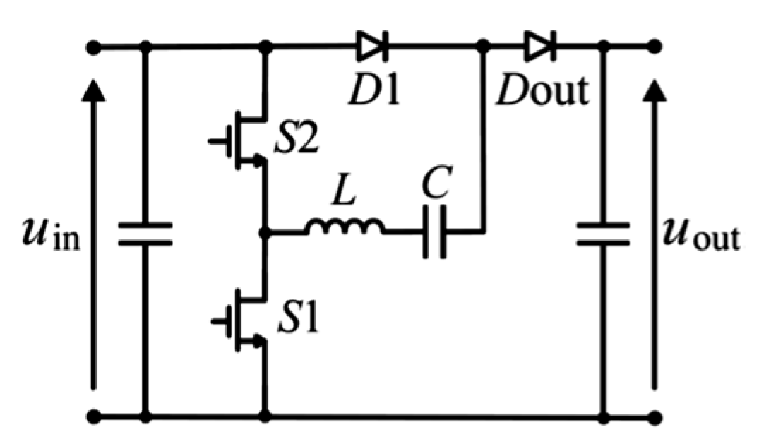
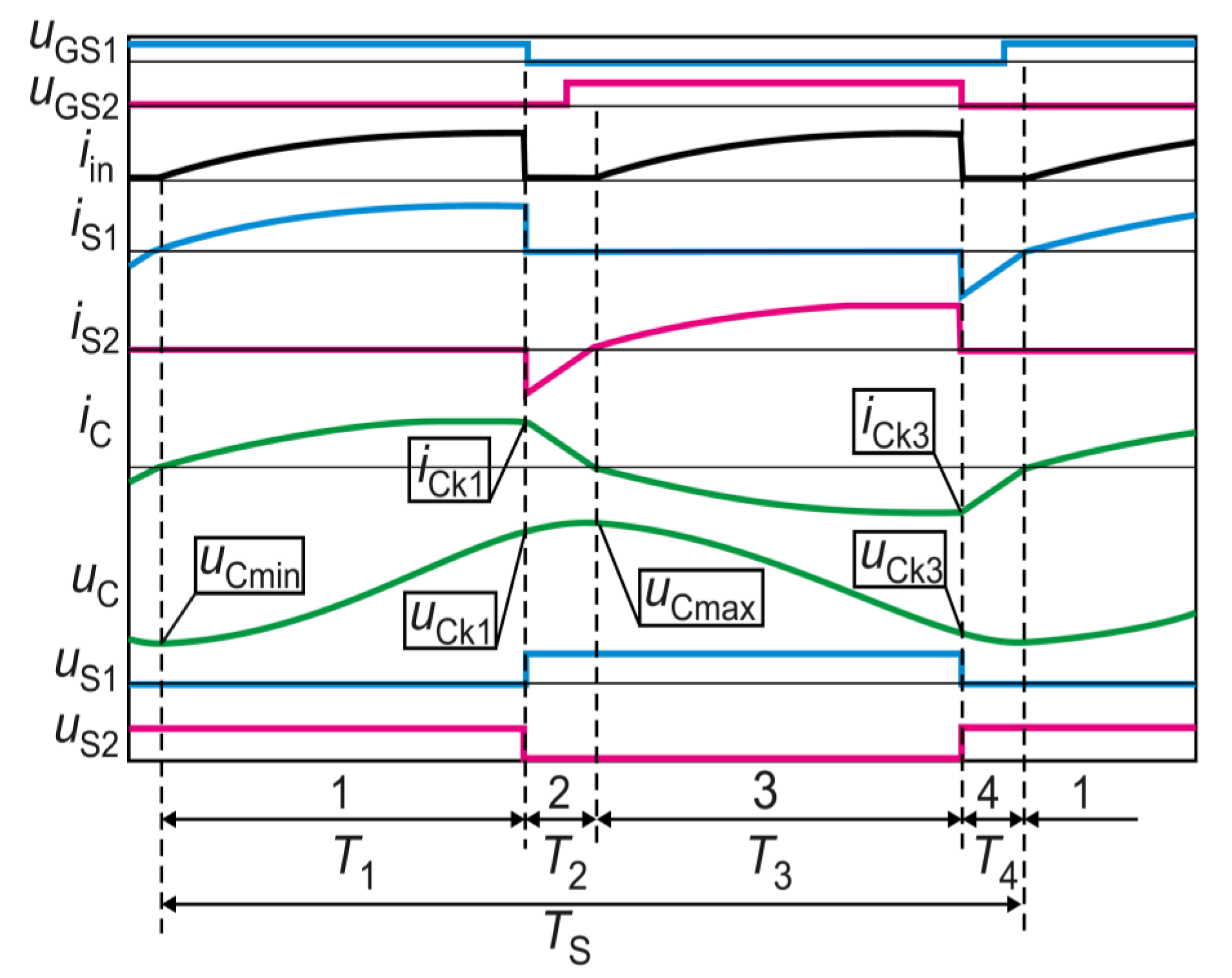
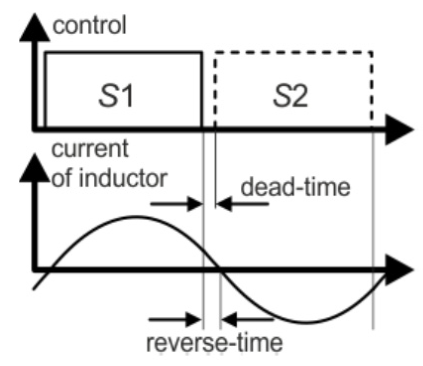
2. Operation Principle of the Resonant Power SCVD

According to the basic principle of the operation of a Switch-Capacitor Voltage Multiplier (SCVM) or an SCVD described in [5,6], the converter operates in the ZCS mode. The topology presented in Figure 1 is explained in [6] and in [2,3] (in the case of a converter equipped with four transistors). Both in the charging and discharging cycle of the switched capacitor, the current oscillates and reaches zero value (Table 1, pattern P1). In such a switching method, the theoretical voltage gain of the SCVD equals
GU = Uout/Uin = 2
In the ZCS mode, conduction losses and switching losses of the SCVD are caused by the discharging of the transistor output capacitance during the turn-on transitions (COSS loss). Using that soft-switching mode, the efficiency of the SCVD has the following analytical model (based on [5]):
η   =   1     π 2 16 P in r U in 2 T S T 1     Δ U D U in     Δ W Sn f S P in
where Uin is the input voltage, Pin is the input power, r denotes the total resistance, both of the circuit of charging and discharging the switched capacitor, including the resistance of the switch, and ΔUD is the voltage drop across each diode, assumed to remain constant in the forward-conducting state. T1 is the conduction time of the transistors, TS is the switching period, fS is the switching frequency, and ΔWSn is the energy lost at turn-ons in the resistances of both the switches in a single switching period.
Figure 1 shows that the voltage on the switches of an SCVD equals the input voltage. However, in an SCVM, the voltages on the switches exceed the input voltage, and they increase in the switching cells nearer to the output [5].
In the case of the application of GaN switches, it is assumed that the converter can operate with very high efficiency under modes when the switches are turned-off while conducting. Therefore, each switching period can consist of four states that are presented in Figure 2.
  • State 1: transistor S2 is switched-off and transistor S1 conducts the source current that charges the switched capacitor (SC);
  • State 2: transistor S1 is switched-off and transistor S2 conducts reversely until the inductance current reaches zero; the charging of the SC is continued in this state;
  • State 3: transistor S1 is switched-off and transistor S2 conducts the current that is forced by the source and the switched capacitor to flow to the output;
  • State 4: transistor S2 is switched-off and transistor S1 conducts reversely until the inductance current reaches zero; the charging of the output capacitor is continued.
Assuming a hard termination of the transistor current, various switching patterns can be proposed (Table 1). Pattern P1 with the ZCS switching is also shown for comparison.
Under the ZVS operation, the inductor current can discharge the capacitance of a switch before it starts flowing in the reverse direction (Figure 3). This can occur when the switch output capacitance is low, because a high-frequency SC converter is designed with a very low parasitic inductance. Therefore, a GaN or a superjunction MOSFET switch is very favorable in such an operating mode, due to short transition times. As the ZVS operation is more efficient than the ZCS switching, pattern P2 appears to be the most attractive. Furthermore, using pattern P2, switching can be achieved in the ZVS and nearly ZCS mode (LCS–low current switching), which is discussed in more detail in Section 4.

3. Output Voltage Control of SCVD

An idea of the output voltage regulation of the SCVD assumes the shortening of the charging and/or discharging process of the switched capacitor. Thus, a lower amount of energy is transferred through this component. At the same time, high efficiency of operation can be achieved by reducing the RMS current and eliminating turn-on losses. Thus, when a wide range of switching frequency is assumed on the stage of the design, pattern P2 (Table 1) seems to be the most favorable, and the operation under this pattern will be further analyzed in more detail.
The analysis below refers both to the switching patterns P2 (T1 + T2 + T3 + T4 = TS, Figure 3) and P3 (T1 + T2 + T3 + T4 < TS) (Table 1). It assumes ideal power electronic switches, fixed values of input voltage Uin and power Pin, equal values of resonant frequency f0 and characteristic impedance ρ of each current path in Figure 2, as well as neglecting parasitic resistances and voltage drops across the power electronic devices, where
ω 0 =   2 π f 0   =   1   / ( L C ) ,   ρ   =   ω 0 L   =   L / C
The capacitor is being charged in states 1 and 2 (Figure 2 and Figure 3). The capacitor current and voltage are described by Equations (4)–(11) (time is counted from zero from the beginning of each state)). They present the current of a typical series LC circuit supplied from a voltage source, and the voltage across its capacitor, taking into account the initial values of the currents and voltages (Figure 3). The capacitor current and the voltage across it are given by
i C ( t ) =   U in   U C min ρ   sin ω 0 t = I m sin ω 0 t
u C ( t ) = U in   ( U in   U C min ) cos   ω 0 t
in cycle 1, with iC (T1) = ICk1, uC(T1) = UCk1, and by (6) and (7)
i C ( t ) =   I C k 1 cos   ω 0 t U C k 1 ρ   sin ω 0 t
u C ( t ) = U C k 1 cos   ω 0 t + ρ   I C k 1 sin ω 0 t
in cycle 2, with iC (T2) = 0, uC(T2) = UCmax.
The capacitor is being discharged in states 3 and 4 (Figure 2 and Figure 3). The capacitor current and voltage are as follows:
i C ( t ) = ( U in   U out +   U C max )   / ρ   sin ω 0 t
u C ( t )   =   U out     U in +   ( U in U out   + U C max )   cos   ω 0 t
in cycle T3, with iC (T3) = ICk3, uC(T3) = UCk3, and
i C ( t ) =   I C k 3 cos ω 0 t   +   ( U out   U C k 3 ) / ρ   sin ω 0 t
u C ( t )   =   U out   ( U out U C k 3 )   cos   ω 0 t   +   ρ   I C k 3 sin ω 0 t
in cycle 4, with iC (T4) = 0, uC(T4) = UCmin.
For further analysis, it is assumed that
T1 = T3, T2 = T4
ICk3 = −ICk1
Im (4) is the amplitude of the input current and the switched capacitor current, and can be calculated based on the expression
I inav = P in U in = 2 T S 0 T 1 I m sin ω 0 t d t   =   1 π   f S f 0 I m [ 1 cos ( 2 π T 1 T 0 ) ]
All the currents and voltages in the SCVD can be computed based on (4)–(14).
Introducing normalized quantities
I _ mn =   I m U in / ρ ,   I _ C k 1 n =   I C k 1 U in / ρ ,   P _ in _ n =   P in U in 2 / ρ U _ Ck 1 n =   U Ck 1 / U in ,   U _ C min n =   U C min / U in ,   U _ C max n =   U C max / U in ,   U _ outn =   U out / U in U _ outn =   U out / U in f _ Sn =   f S / f 0 ,   T _ 1 n = T 1 / T S ,   T _ 2 n =   T 2 / T S
we obtain
I _ mn   = π P _ in - n / f _ Sn 1     cos ( 2 π T _ 1 n / f _ Sn ) ,   I _ C k 1 n =   I _ mn sin ( 2 π T _ 1 n / f _ S n )
U _ C min n =   1     I _ mn ,   U _ C k 1 n   =   1     I _ mn cos ( 2 π T _ 1 n / f _ S n )
T _ 2 n =   f _ Sn arctg ( I _ C k 1 n / U _ C k 1 n )   / ( 2 π )
U _ C max n = U _ C k 1 n cos ( 2 π T _ 2 n / f _ S n ) +   I _ C k 1 n sin ( 2 π T _ 2 n / f _ S n )
U _ outn =   U _ C min n   + U _ C max n ,   U _ C k 3 n   = U _ outn   U _ C k 1 n

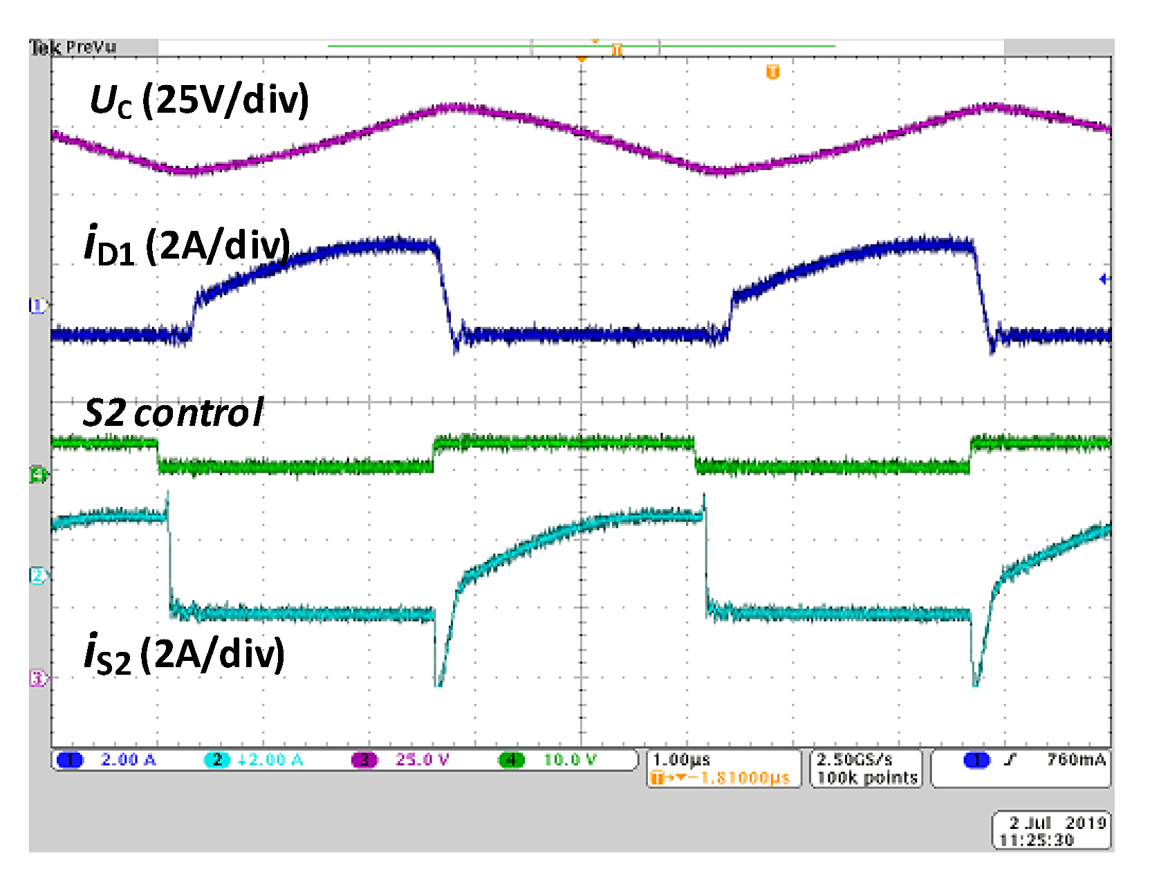
3.1. Pattern P2—Continuous Capacitor Current Mode

The capacitor current is continuous if T1 + T2 + T3 + T4 = TS (pattern P2—Table 1 and Figure 3), which corresponds to (12)
TS = 2(T1 + T2)
This switching pattern can be easily obtained by varying TS and using long gate pulses, as shown in Table 1 for pattern P2–times T1 and T2 (Figure 3) will be set automatically.
Using (16)–(20) and taking into account that (21) T2n = ½ – T1n yields
π ( 1 2 T _ 1 n ) = f _ Sn arctg [ π P _ in - n / f _ Sn sin ( 2 π T _ 1 n / f _ Sn ) 1     ( 1 + π P _ in - n / f _ Sn )   cos ( 2 π T _ 1 n / f _ Sn ) ]
From (22), normalized conduction time T1n = T1/TS of the transistor can be computed numerically. Figure 4 presents T1n (a), and normalized output voltage Uoutn (b) as a function of fSn for three values of Pin-n = Pin/(Uin2/ρ): 0.0344, 0.0688, and 0.1031. The value of Pin-n = 0.0688 corresponds to, e.g.,: Uin = 200 V, Pin = 400 W, and ρ = 6.876, which can be obtained for, e.g., L = 10.4 μH and C = 0.22 μF. These parameters correspond to those of the experimental setup presented in Section 6.
In switching pattern P2, the theoretical lower limit of the normalized switching frequency fSn is 1, which corresponds to switching pattern P1 (Table 1) with zero dead-times. The upper limit of fSn results from (21), and it depends on power, which can be seen in Figure 4.
The normalized conduction time T1/TS of the transistors decreases with increasing frequency, and the power is larger as the decrease rate is higher. Moreover, it is very important that varying fS affects the output voltage. In switching pattern P2, it is possible to control the output voltage in the range of ca. 1.45 Uin to 2 Uin. An increase in fS results in decreasing voltage gain [see Figure 4b]. As in the case of T1/TS, the larger the power, the higher the decrease rate.
In the discussed switching pattern P2, the capacitor is never discharged to zero volts.

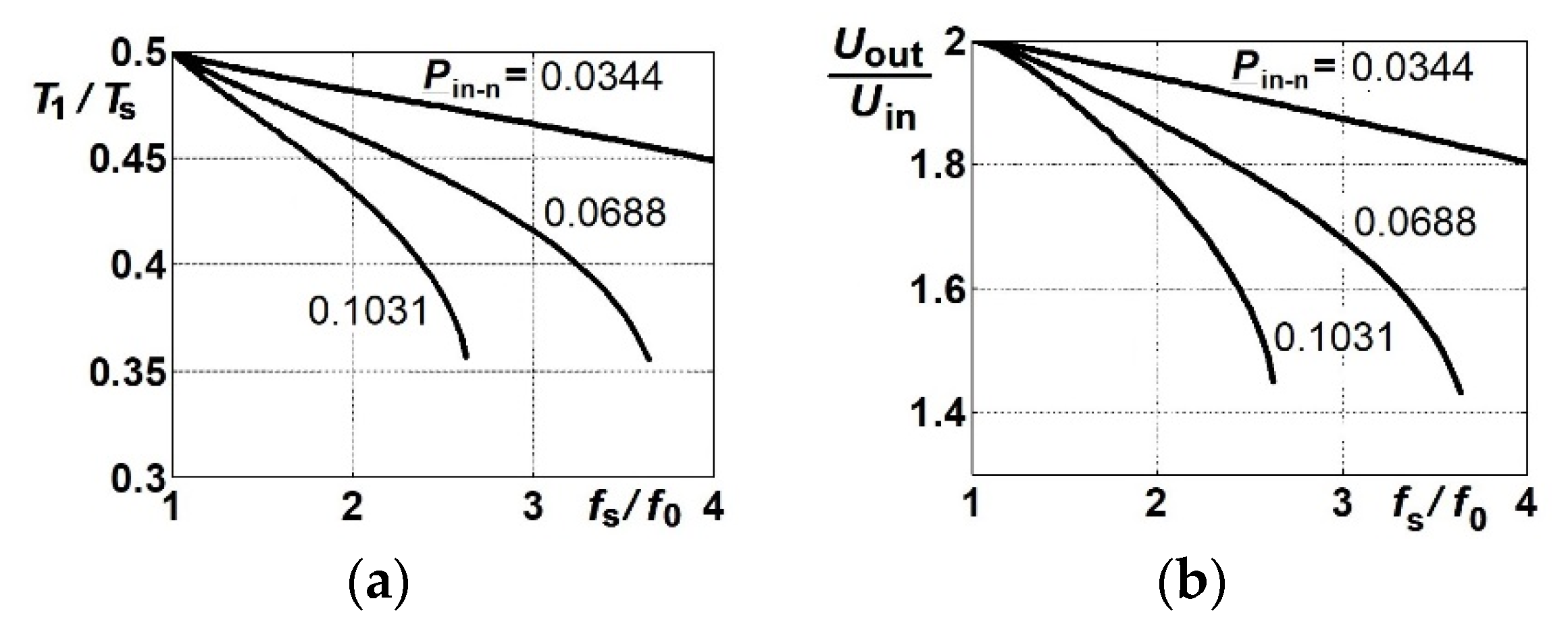
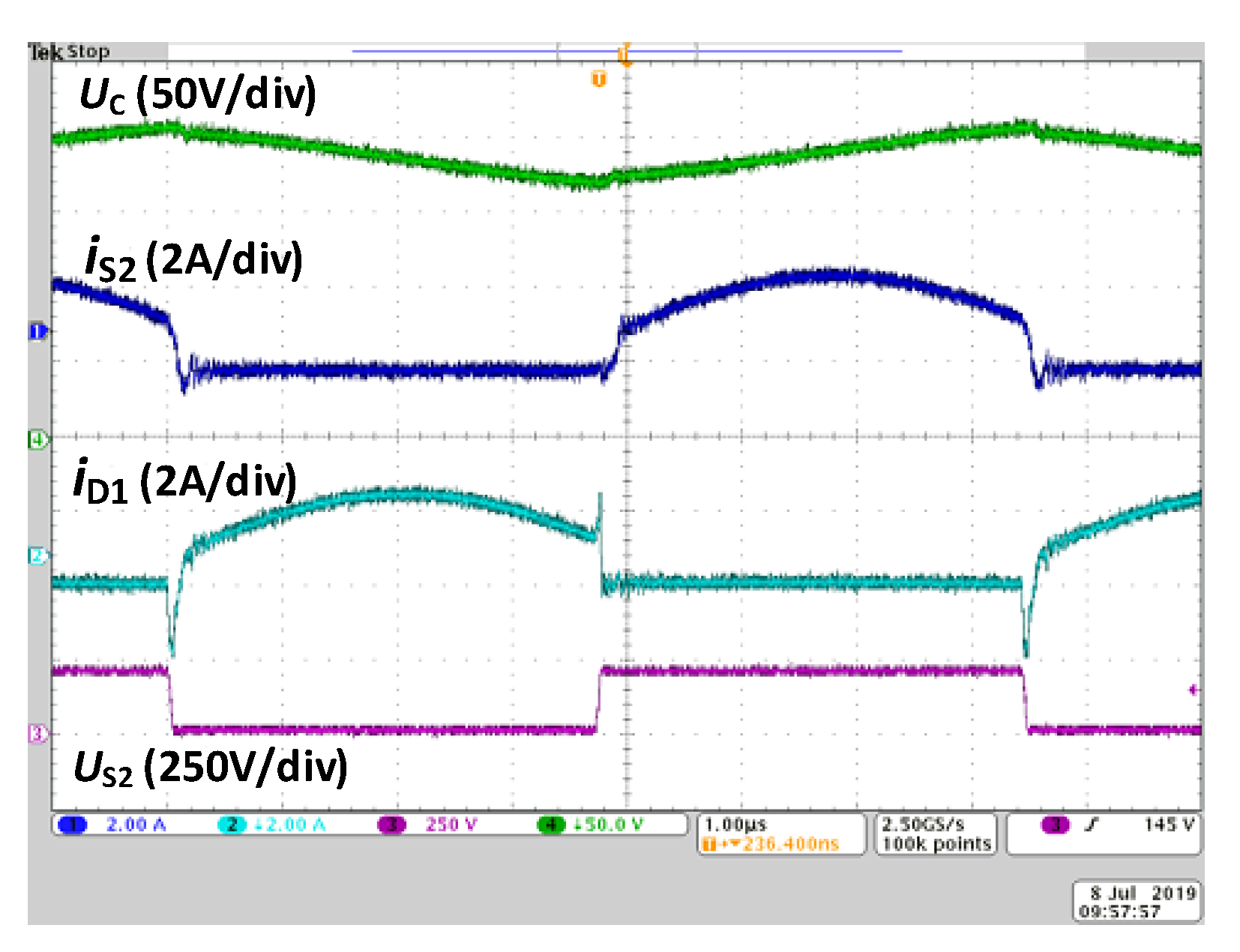
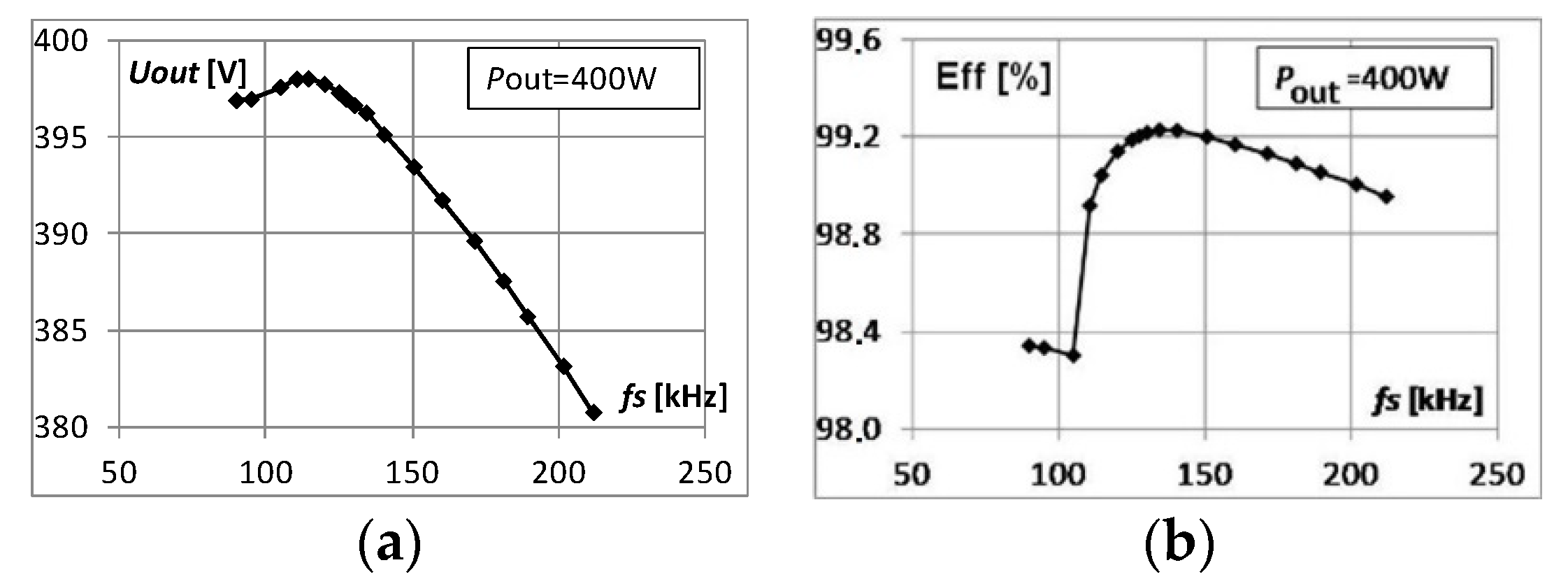
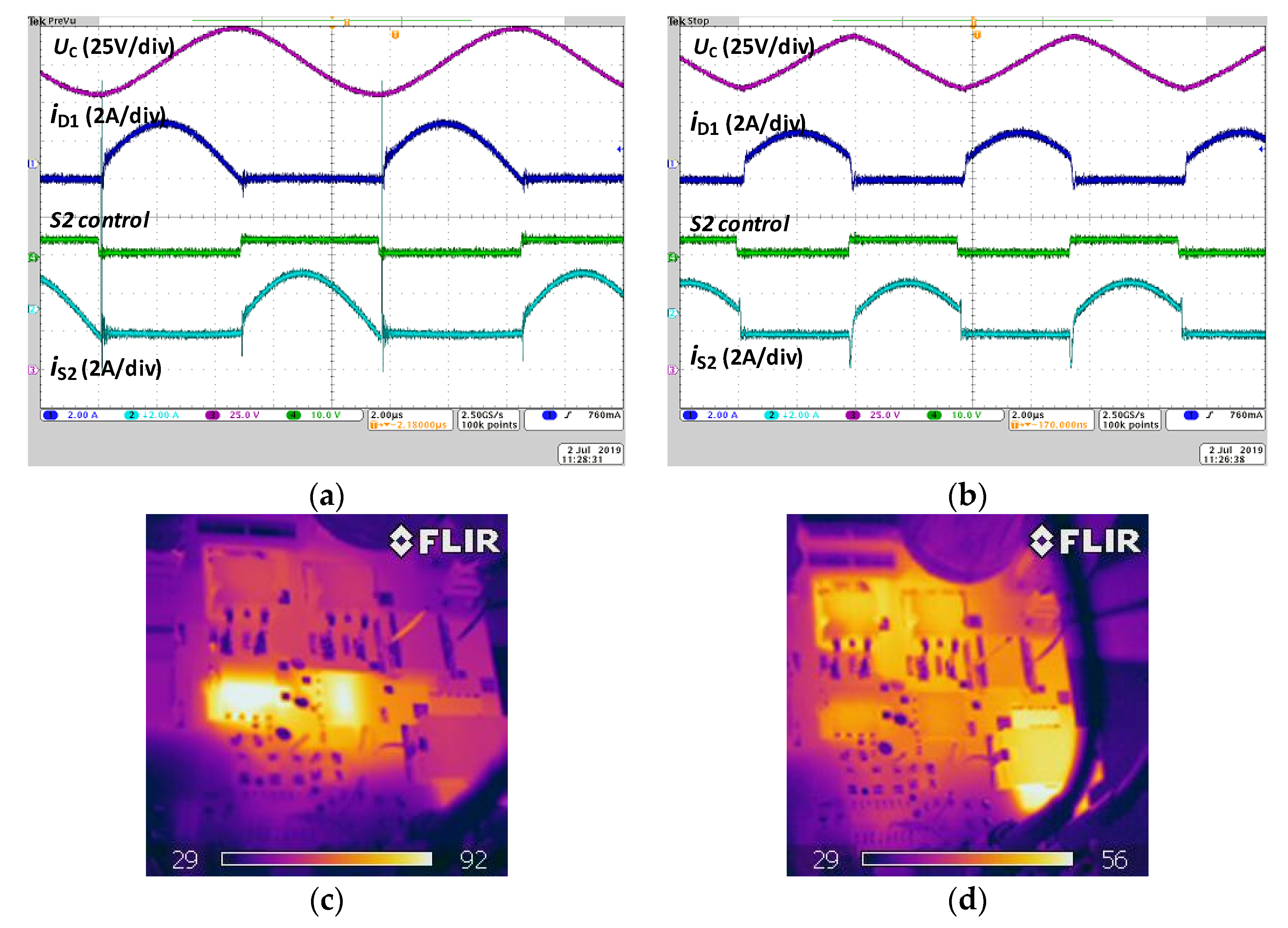
3.2. Pattern P3—Discontinuous Capacitor Current Mode

The continuous current mode is advantageous in terms of optimizing the converter’s efficiency. However, the converter can also be operated at a fixed frequency fS by varying the conduction time T1 of the transistors. If T1n = T1/TS is lower than that in Figure 4a, the capacitor current becomes discontinuous–pattern P3 in Table 1. This operating mode offers a wider range of output voltage control.
The conduction time T1 of the transistors is limited. Its maximum normalized value is equal to that shown in Figure 4a and its minimum value is limited by two factors. The first is the condition U C min   0 , leading to
T _ 1 min - n   =   T 1 min   / T S   =   f _ Sn / ( 2 π )   arccos ( 1 π P _ in - n / f _ S n )
The second factor is the requirement for Uoutn ≥ 1, which results from the topology (Figure 1).
The output voltage regulation can be done by varying transistor conduction time T1 at a given frequency fS, where a decrease in T1 leads to a decrease in the voltage gain ratio (Figure 5). This ratio falls with the rise of frequency fS. Moreover, Uout is lower at higher powers.

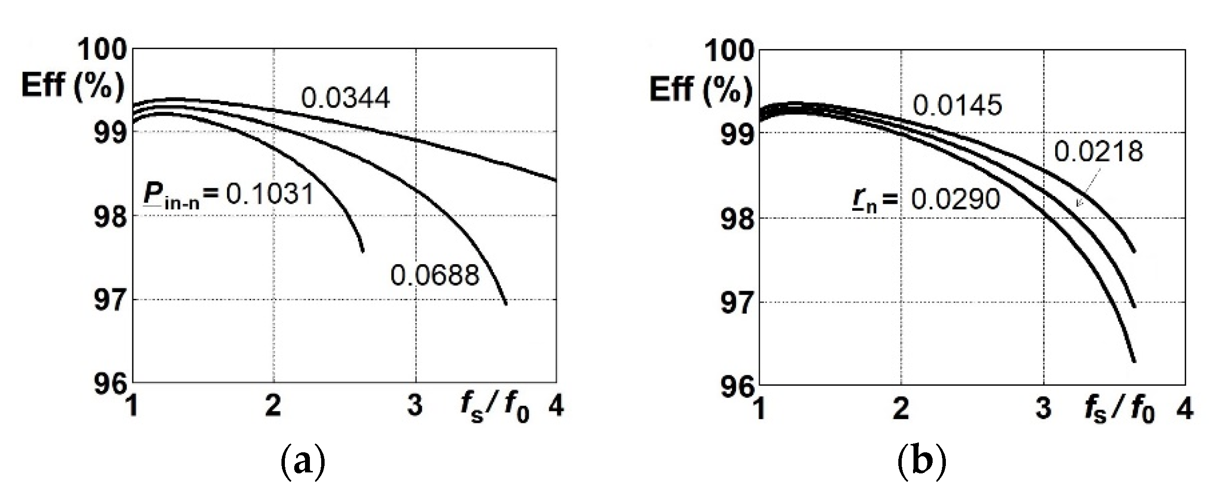
4. Efficiency of the SCVD

4.1. Model of Efficiency of the SCVD–Maximum Efficiency of the Converter without Switching Losses

The efficiency of the SCVD is determined by the resistance of its components, voltage drops on the diodes, input voltage, power, operating frequency, and the switching pattern. The following calculations have been performed for the SCVD with GaN switches using pattern P2 (Table 1). The assumptions for the analysis given in Section 3 remain valid, except for taking into account the circuit parasitic resistances, which are now added to the transistor resistances, and voltage drops on the diodes. Moreover, the conduction losses in the GaN transistors are computed taking into account its RDS(on), both for forward and reverse conduction. This can be done as the gate signals are applied during nearly the half-period TS/2, except for dead-time, which is very short.
The current iS1(t) in transistor S1 is equal to the capacitor current iC(t) in state 4 (reverse conduction) and state 1 (forward conduction), and equal to zero in states 2 and 3 (Figure 2 and Figure 3). The current iS2(t) in transistor S2 is phase-shifted, having the same shape and values. The RMS value of both currents is the same. It can be calculated from
I S   =   1 T S 0 T S i S 1 2 ( t ) d t   =   1 T S [ 0 T 1 i S 1 ( 1 ) 2 ( t ) d t   +   0 T 4 i S 1 ( 4 ) 2 ( t ) d t   ]
where iS1(1)(t) = iC(t) in state 1 (4), iS1(4)(t) = iC(t) in state 4 (10), and T4 = T2 (12). After calculating the integrals using the equations mentioned above, and taking into account relationship (13), current IS can be presented in the form
I S   =   I S A 2 + I S B 2 + I S C 2 + I S D 2 .
where
I S A 2 =   I C k 1 2 2 [ T _ 2 n +   f _ S n   4 π sin ( 4 π T _ 2 n / f _ S n ) ] I S B 2 =   f _ Sn   4 π I C k 1 U C k 3   U out ρ [ 1 cos ( 4 π T _ 2 n / f _ S n ) ] I S C 2 = ( U C k 3   U out ) 2 2 ρ 2   [ T _ 2 n   f _ Sn   4 π sin ( 4 π T _ 2 n / f _ S n ) ] I S D 2 = ( U in   U Cmin ) 2 2 ρ 2   [ T _ 1 n   f _ Sn   4 π sin ( 4 π T _ 1 n / f _ S n ) ] .
The current iD1(t) in diode D1 is equal to the capacitor current iC(t) in states 1 and 2, and equal to zero in states 3 and 4 (Figure 2 and Figure 3). The current iDout(t) in diode Dout is phase-shifted, having the same shape and values as iD1(t). The average value of both currents is the same and equal to
I D av   =   1 T S 0 T S i D 1 ( t ) d t   =   1 T S   [ 0 T 1 i D ( 1 ) ( t ) d t   +   0 T 2 i D ( 2 ) ( t ) d t ]
where iD1(1) = iC(t) in state 1 (4) and iD1(2) = iC(t) in state 2 (6).
I D av   =   f _ Sn   2 π { I m [   1     cos ( 2 π T _ 1 n / f _ S n ) ] +   I C k 1 sin ( 2 π T _ 2 n / f _ S n ) U C k 1 ρ   [   1 cos ( 2 π T _ 2 n / f _ S n ) ] }
Conduction losses ΔPC are the sum of losses in the transistors and the diodes
Δ P C =   ( r 1 + r 2 )   I S 2   +   ( Δ U D 1 + Δ U D out )   I D av
where r1 and r2 denote the total resistance, including the resistance of the transistor, in the circuits with S1 and S2, respectively; ΔUD1 is the voltage drop across diode D1, and ΔUDout is the voltage drop across diode Dout (Figure 1). It is assumed that the voltage drops across the diodes remain constant in the conducting state. Therefore, the efficiency is
η =   1   Δ P C P in   =   1     ( r 1 + r 2 ) I S 2 P in     ( Δ U D 1 + Δ U D out ) I D av P in
If the resistances and diode voltage drops are the same, i.e.;
r 1   =   r 2   =   r ,   Δ U D 1 = Δ U D out = Δ U D
we can rewrite the efficiency formula in the form
η =   1     2 (   r _ n I _ S n 2   +   Δ _ U D n I _ D avn )   / P _ in - n  
where
I _ S n =   I S U in / ρ ,   I _ D avn =   I D av U in / ρ ,   r _ n   =   r / ρ ,   Δ U _ D n = Δ U D / U in
Figure 6 presents the model of efficiency created on the basis of (32). The peak efficiency achieves a maximum above the resonant frequency. It is assumed that the switching losses are reduced in this area as well.

4.2. The Switching Concept for Maximum Efficiency

The advantages of the application of the GaN switches in the proposed high-frequency SCVD results from the possibility of using the ZVS mode with low switching losses under the operation above the resonant frequency (low COSS of the switch and short transition time). It can be assumed that the most favorable case of operation (ZVS), from the efficiency point of view, is achieved by turning-off the transistors just before their current reaches zero. The reverse conduction of the transistors should be as short as possible (Figure 7). When the transistors turn off near the zero crossings of the current, the turn-off loss can be neglected. In an SC converter such as the SCVD, with very small inductors, the application of a GaN switch will make it possible to achieve a highly improved efficiency in the ZVS mode keeping both the dead-dime and reverse-time very short.

5. Mixed Switching Patterns in Applications

To obtain a functional converter with efficient and effective voltage regulation, various switching patterns can be utilized depending on the operational conditions. Furthermore, the proposed switching patterns can be effectively used in more complex systems created on the basis of the SCVD.

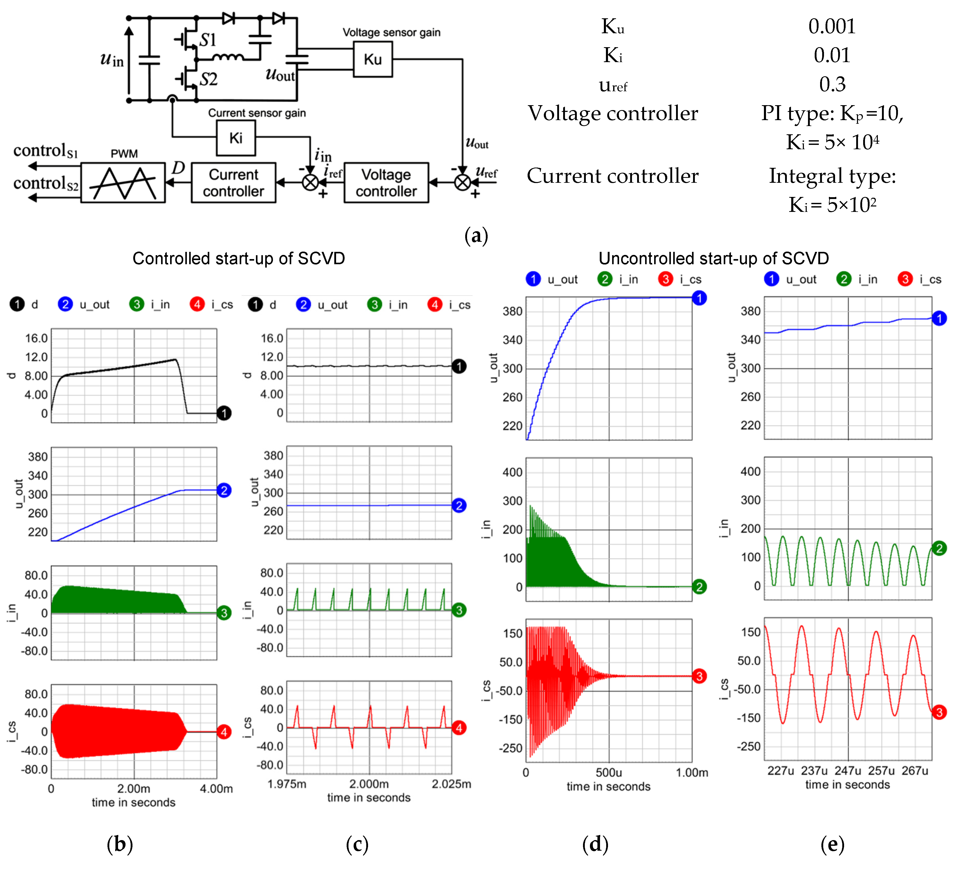
5.1. Start-Up of the Converter

During the start-up of the converter, the SCVD is usually overloaded when pattern P1 is used. The maximum power (Pmax) of this type of voltage multiplier is proportional to the switching frequency and the switched capacitance C [5]. Under pattern P1, the converter can increase the power as far as the switched capacitor is not fully discharged in a switching period. The operation of an SCVD with partial discharge and low voltage ripples under the rated power requires the use of a large-enough switched capacitor (C). In this case, the converter’s power is Pnom << Pmax. When the switches, diodes and the PCB are designed for nominal power Pnom, the converter can easily be overloaded. To overcome this issue in conditions of overloading, such as the start-up of the converter, other switching patterns can be used. Figure 8 presents a comparison of waveforms during the start-up with pattern P3 and pattern P1. From these results, it is seen that the overloading of the converter is significantly limited by the appropriate use of the proposed switching pattern P3.
Pattern P3 can be easily achieved in a classic PWM generator (it requires a constant switching frequency and a variable duty ratio). The implementation of this pattern can be achieved by the use of VCO (Voltage Controlled Oscillator), and pattern P4 could require a special hardware design (e.g., in FPGA technology).

5.2. Bi-Directional Converter

A synchronous SCVD makes it possible to convert energy in both directions, which is required in systems with batteries. When the voltages on both sides are constant, the converter should be able to regulate the voltage gain in both directions. Figure 9 presents the concept of such a synchronous SCVD, the most suitable switching pattern (P4), and its operating states. The operation occurs in the following three states (Figure 9b):
(1)
In the first state, the SC is being charged from the output voltage source. This state is terminated by turning off the switches S1 and S4;
(2)
State 2—the inductor current goes to zero via S2 and S3 (reverse conduction);
(3)
In state 3—turning on S3 starts an oscillation in a new circuit, and the energy is transferred to the input source. This is advantageous since the oscillation continues until the inductor current reaches zero. Breaking this oscillation by switching off S3 would start the current flow to the output and charging the output, which would not be favorable to the efficiency of the conversion.
Pattern P4 guarantees a proper operation of the synchronous SCVD, which is confirmed by the steady-state waveforms presented in Figure 9. It assures ZVS of switch S3, ZCS turn-on of S1 and S4, voltage regulation and unidirectional currents of the sources. Other switching patterns enable a bi-directional energy transfer with voltage regulation, but with an unrequired current recirculation between SC and the sources.

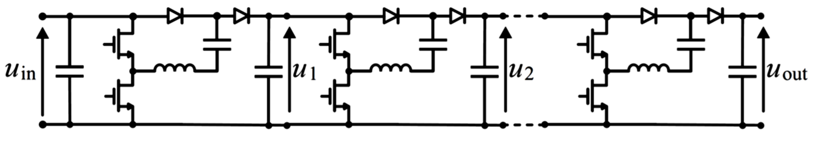
5.3. A Series-Connected High-Voltage-Gain System

A section containing capacitors allows for designing modular [23] and cascaded [26,27] converters, where such parameters as the output voltage regulation can be improved. In [27], modular converters composed of series-parallel sections are analyzed. It has been proven there that the series-connected voltage doublers (Figure 10) are the most effective voltage multiplier topology taking into consideration the relation of the number of switches to the voltage gain.
The SCVD series achieves the voltage gain GU = 2n, where n is the number of the SCVD converters. In an SCVD series (Figure 10), each internal converter operates in different conditions (voltage and current stress). By suitable use of the proposed switching patterns, the SCVD series can achieve novel unique features such as output voltage regulation and very high efficiency. The most effective mixed switching pattern can depend on such parameters as switching frequency or load. Table 2 presents examples of scenarios for a decision on implementing optimal switching patterns.

6. Experimental Setup and Test Results

The experimental investigations have been performed in the setup with parameters presented in Table 3 using the equipment listed in Table 4. The efficiency of the GaN-Based DC–DC resonant boost converter was determined using Yokogawa WT1800 power analyzer [35] on the basis of the output to the input power ratio. The range of voltages and currents in the tested converter allows for the use of the internal current and voltage sensors (5 A and 600 V) and achieving an adequate precision of the measurements.
The measurements were intended to verify the basic concepts presented in this paper: the switching strategies and efficiency of the SCVD converter shown in Figure 1. The obtained results confirm the proper operation of the converter under various switching strategies and its high efficiency.

6.1. Switching Pattern P2–Operation with Continuous Capacitor Current Mode

Figure 11 presents examples of selected time waveforms in switching pattern P2. A dead-time of 50 ns has been used; thus, after the turn-off of each transistor, the other transistor begins conducting (reverse conduction and, next, forward conduction) with nearly zero turn-on loss and low conduction loss.

6.2. Comparison of Operation in the ZCS Mode (Pattern P1) and ZVS Mode (Pattern P2)

A comparison of the operation below resonant frequency (ZCS) and above that frequency (ZVS) confirms the concept of operation with high efficiency and output voltage control.
Figure 12 presents the operation of the converter in the ZVS and nearly in the ZCS mode. In these conditions, maximum efficiency is achieved. The ZVS mode is maintained, although the negative current of S2 is not as clearly visible as in Figure 11. Before the switch S2 is turned on, it conducts a negative current and its voltage is zero. On the other hand, the full ZCS mode is visible in Figure 15a.
Figure 13 presents graphs of voltage gain end efficiency versus switching frequency fS. The efficiency chart (Figure 13b) clearly shows a substantial increase in efficiency when the operating mode changes from the switching pattern P1 to P2. The peak efficiency occurs slightly above f0. A further increase in the switching frequency leads to a decrease in output voltage (voltage gain regulation) and results in a decrease in efficiency.
Figure 14a–d present the charts of efficiency of the SCVD versus output power for various values of the switching frequency under pattern P2. Figure 14e depicts the relation between the efficiency and the gain, obtained from the data in Figure 13. The highest achieved efficiency is 99.228% at fS = 134.4 kHz and Pout = 396.23 W.
Further analysis of the ZVS concept in the SCVD, achieved by the introduction of pattern P2, is presented by comparing the waveforms and thermograms of the converter operating in accordance with patterns P2 and P1. The comparison is presented in Figure 15 for Pout = 400 W. The IR photos confirm considerably lower losses and heat generation in the transistors when the converter operates using pattern P2 [see Figure 15b,d] versus the case of the ZCS switching with pattern P1 [see Figure 15a,c].
Figure 16 confirms the proper operation of the converter in switching pattern P3. The inverter operates in discontinuous conduction mode (DCM). Output voltage regulation is possible at a constant switching frequency (Table 1).
Table 5 shows a comparison of the maximum efficiencies of selected converters presented in recently published papers. The power at that the maximum efficiency was registered, and the type of switches that were used are also listed. (RSCC–resonant switched-capacitor converter, RTBSCC–resonant two-switch boosting switched-capacitor converter, IBC–intermediate bus converter, MRSCC–multilevel resonant switched-capacitor converter). The efficiency of the converter presented in this paper is one of the highest that are reported in the recent bibliography.

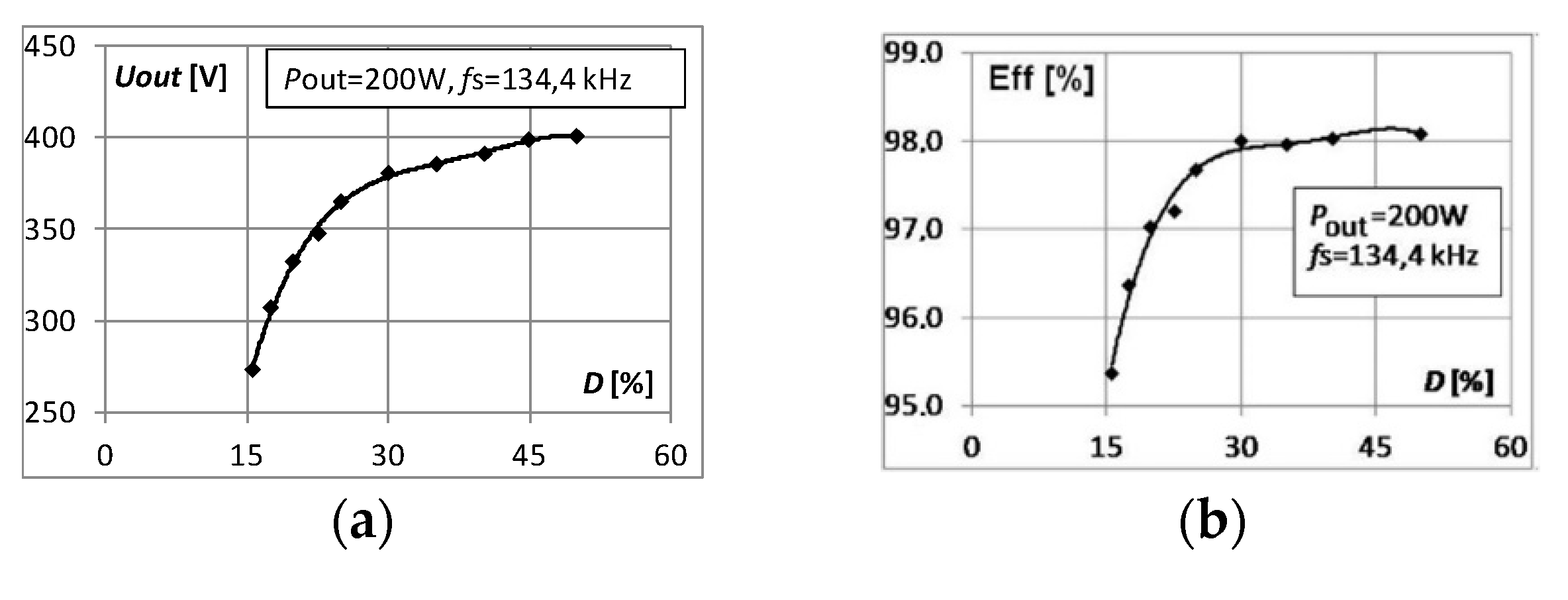
6.3. Output Voltage Regulation by the Switching Pattern P3

The most suitable method for the output voltage regulation in an SCVD is pattern P3, where the capacitor current is discontinuous (Figure 16). Very good effectiveness of the regulation is confirmed in Figure 17 which shows the output voltage versus duty cycle D defined as the ratio of the turn-on time T1 of a transistor to the switching period TS. A wide range of the output voltage is achievable with an acceptable efficiency deterioration at low values of the duty cycle.

7. Conclusions

In this paper, the concepts of control for a resonant switched-capacitor voltage doubler are presented. They allow the use of the SCVD converter as a fully functional DC–DC converter with output voltage regulation and very high efficiency.
A classic SCVM operates in the ZCS mode, in which switching power losses associated with COSS of the transistors are significant. The application of GaN switches makes it possible to operate with a high frequency while maintaining high efficiency. However, the efficiency can be significantly improved by the proposed switching patterns of the converter, where the reverse conduction occurs to achieve zero-voltage turn-on of the transistors. The maximum efficiency that was measured in the demonstrated setup exceeds 99.2%. The heat generation in the transistors is reduced significantly as well. In the switching pattern dedicated to maximum efficiency, an output voltage adjustment is possible. In another switching pattern (P3) proposed in this paper, the SCVD converter achieves a very high output voltage regulation range. The developed model of losses matches the experimental results and can be used in the design process. In addition, the results can be applied in other topologies of the SC converters.
The switching pattern P2 allows for a significant improvement in the efficiency of the SCVD by COSS loss reduction. To accomplish that, very fast switching is required because the cycle sequence: turn-off/dead-time/turn-on should occur on the falling slope of the resonant current, taking only a small part of the oscillation time. The SCVD is a switched-capacitor converter with low resonant inductance, therefore the oscillation time is very short. Three types of switches (superjunction MOSFET, GaN, and SiC) as a prospective adequate solution for high-efficiency operation of the SCVD. Taking into consideration the features of GaN switches, the experimental tests have been performed with the use of GaN GIT switches. The switching pattern P3 allows for easy implementation for overcurrent limitation of the start-up of the converter, and pattern P4 can be used in the bi-directional operation of the synchronous SCVD. Various patterns can be also combined in the cascaded high-voltage-gain system composed of several SCVDs.

Author Contributions

Conceptualization, R.S.; methodology, R.S., Z.W., A.M., A.S. and A.P.; software, R.S., Z.W., A.P., and A.S.; validation, R.S., and Z.W.; formal analysis, R.S., Z.W.; investigation, R.S., Z.W., A.M., A.S. and A.P.; resources, R.S.; data curation, R.S., Z.W., A.M., and A.S.; writing—original draft preparation, R.S., and Z.W.; writing—review and editing; visualization, R.S. and Z.W.; supervision, R.S. and Z.W.; project administration, R.S. All authors have read and agreed to the published version of the manuscript.

Funding

This research received no external funding.

Conflicts of Interest

The authors declare no conflict of interest.

References

  1. Ioinovici, A. Switched-capacitor power electronics circuit. IEEE Circuits Syst. Mag. 2001, 1, 37–42. [Google Scholar] [CrossRef]
  2. Sano, K.; Fujita, H. Performance of a high-efficiency switched-capacitor-based resonant converter with phase-shift control. IEEE Trans. Power Electron. 2011, 26, 344–354. [Google Scholar] [CrossRef]
  3. Vasić, M.; Serrano, D.; Toral, V.; Alou, P.; Oliver, J.A.; Cobos, J.A. Ultraefficient Voltage Doubler Based on a GaN Resonant Switched-Capacitor Converter. IEEE J. Emerg. Sel. Top. Power Electron. 2019, 7, 622–635. [Google Scholar] [CrossRef]
  4. Cervera, A.; Evzelman, M.; Mordechai Peretz, M.; Ben-Yaakov, S. A high-efficiency resonant switched capacitor converter with continuous conversion ratio. IEEE Trans. Power Electron. 2015, 30, 1373–1382. [Google Scholar] [CrossRef]
  5. Waradzyn, Z.; Stala, R.; Mondzik, A.; Penczek, A.; Skala, A.; Pirog, S. Efficiency analysis of MOSFET-based air-choke resonant DC–DC step-up switched-capacitor voltage multipliers. IEEE Trans. Ind. Electron. 2017, 64, 8728–8738. [Google Scholar] [CrossRef]
  6. Mondzik, A.; Waradzyn, Z.; Stala, R.; Penczek, A. High efficiency switched capacitor voltage doubler with planar core-based resonant choke. In Proceedings of the 2016 10th International Conference on Compatibility, Power Electronics and Power Engineering (CPE-POWERENG), Bydgoszcz, Poland, 29 June–1 July 2016; pp. 402–409. [Google Scholar] [CrossRef]
  7. Stala, R.; Waradzyn, Z.; Penczek, A.; Mondzik, A.; Skala, A. A Switched-Capacitor DC-DC Converter with Variable Number of Voltage Gains and Fault-Tolerant Operation. IEEE Trans. Ind. Electron. 2019, 66, 3435–3445. [Google Scholar] [CrossRef]
  8. Evzelman, M.; Ben-Yaakov, S. Average-current-based conduction losses model of switched capacitor converters. IEEE Trans. Power Electron. 2013, 28, 3341–3352. [Google Scholar] [CrossRef]
  9. Ye, Y.; Cheng, K.W.E. A family of single-stage switched-capacitor–inductor PWM converters. IEEE Trans. Power Electron. 2013, 28, 5196–5205. [Google Scholar] [CrossRef]
  10. Wu, G.; Ruan, X.; Ye, Z. Nonisolated high step-up DC-DC converters adopting switched-capacitor cell. IEEE Trans. Ind. Electron. 2015, 62, 383–393. [Google Scholar] [CrossRef]
  11. Tang, Y.; Wang, T.; Fu, D. Multicell switched-inductor/switched-capacitor combined active-network converters. IEEE Trans. Power Electron. 2015, 30, 2063–2072. [Google Scholar] [CrossRef]
  12. Rosas-Caro, J.C.; Ramirez, J.M.; Peng, F.Z.; Valderrabano, A. A DC-DC multilevel boost converter. IET Power Electron. 2010, 3, 129–137. [Google Scholar] [CrossRef]
  13. Li, S.; Xiangli, K.; Zheng, Y.; Smedley, K.M. Analysis and design of the ladder resonant switched-capacitor converters for regulated output voltage applications. IEEE Trans. Ind. Electron. 2017, 64, 7769–7779. [Google Scholar] [CrossRef]
  14. Li, S.; Zheng, Y.; Wu, B.; Smedley, K.M. A Family of Resonant Two-Switch Boosting Switched-Capacitor Converter With ZVS Operation and a Wide Line Regulation Range. IEEE Trans. Power Electron. 2018, 33, 448–459. [Google Scholar] [CrossRef]
  15. Alam, M.K.; Khan, F.H. A high-efficiency modular switched-capacitor converter with continuously variable conversion ratio. In Proceedings of the IEEE 13th Workshop on Control and Modeling for Power Electronics (COMPEL), Kyoto, Japan, 10–13 June 2012; pp. 1–5. [Google Scholar] [CrossRef]
  16. Ye, Y.; Cheng, K.W.E.; Liu, J.; Ding, K. A step-up switched-capacitor multilevel inverter with self-voltage balancing. IEEE Trans. Ind. Electron. 2014, 61, 6672–6680. [Google Scholar] [CrossRef]
  17. Shen, M.; Peng, F.Z.; Tolbert, L.M. Multilevel DC–DC Power Conversion System with Multiple DC Sources. IEEE Trans. Power Electron. 2008, 23, 420–426. [Google Scholar] [CrossRef]
  18. Gunasekaran, D.; Qin, L.; Karki, U.; Li, Y.; Peng, F.Z. A Variable (n/m)X Switched Capacitor DC–DC Converter. IEEE Trans. Power Electron. 2017, 32, 6219–6235. [Google Scholar] [CrossRef]
  19. Gunasekaran, D.; Qin, L.; Karki, U.; Li, Y.; Peng, F.Z. Multi-level capacitor clamped DC-DC multiplier/divider with variable and fractional voltage gain—An (n/m)X DC-DC converter. In Proceedings of the 2016 IEEE Applied Power Electronics Conference and Exposition (APEC), Long Beach, CA, USA, 20–24 March 2016; pp. 2525–2532. [Google Scholar] [CrossRef]
  20. Gunasekaran, D.; Han, G.; Peng, F.Z. Control methods to achieve soft-transition of gains for a variable (n/m)X converter. In Proceedings of the 2017 IEEE Applied Power Electronics Conference and Exposition (APEC), Tampa, FL, USA, 26–30 March 2017; pp. 3365–3372. [Google Scholar] [CrossRef]
  21. Khan, F.H.; Tolbert, L.M. Multiple-Load–Source Integration in a Multilevel Modular Capacitor-Clamped DC–DC Converter Featuring Fault Tolerant Capability. IEEE Trans. Power Electron. 2009, 24, 14–24. [Google Scholar] [CrossRef]
  22. Bento, F.; Cardoso, A.J.M. Fault tolerant DC-DC converters in DC microgrids. In Proceedings of the 2017 IEEE Second International Conference on DC Microgrids (ICDCM), Nuremburg, Germany, 27–29 June 2017; pp. 484–490. [Google Scholar] [CrossRef]
  23. Setiadi, H.; Fujita, H. Reduction of Switching Power Losses for ZVS Operation in Switched-Capacitor-Based Resonant Converters. IEEE Trans. Power Electron. 2021, 36, 1104–1115. [Google Scholar] [CrossRef]
  24. Xie, W.; Brown, B.Y.; Smedley, K. Multilevel Step-down Resonant Switched-Capacitor Converters with Full-range Regulation. IEEE Trans. Ind. Electron. 2020. [Google Scholar] [CrossRef]
  25. Beck, Y.; Singer, S.; Martinez-Salamero, L. Modular realization of capacitive converters based on general transposed series–parallel and derived topologies. IEEE Trans. Ind. Electron. 2014, 61, 1622–1631. [Google Scholar] [CrossRef]
  26. Zamiri, E.; Vosoughi, N.; Hosseini, S.H.; Barzegarkhoo, R.; Sabahi, M. A new cascaded switched-capacitor multilevel inverter based on improved series-parallel conversion with less number of components. IEEE Trans. Ind. Electron. 2016, 63, 3582–3594. [Google Scholar] [CrossRef]
  27. Stala, R.; Piróg, S. DC–DC boost converter with high voltage gain and a low number of switches in multisection switched capacitor topology. Arch. Electr. Eng. 2018, 67, 617–627. [Google Scholar]
  28. Dalla Vecchia, M.; Ravyts, S.; Van den Broeck, G.; Driesen, J. Gallium-Nitride Semiconductor Technology and Its Practical Design Challenges in Power Electronics Applications: An Overview. Energies 2019, 12, 2663. [Google Scholar] [CrossRef] [Green Version]
  29. Neumayr, D.; Guacci, M.; Bortis, D.; Kolar, J.W. New calorimetric power transistor soft-switching loss measurement based on accurate temperature rise monitoring. In Proceedings of the 29th International Symposium on Power Semiconductor Devices and IC’s (ISPSD), Sapporo, Japan, 28 May–1 June 2017; pp. 447–450. [Google Scholar] [CrossRef]
  30. Li, K.; Evans, P.; Johnson, M. SiC/GaN power semiconductor devices: A theoretical comparison and experimental evaluation under different switching conditions. IET Electr. Syst. Transp. 2018, 8, 3–11. [Google Scholar] [CrossRef] [Green Version]
  31. Kawa, A.; Stala, R. SiC-Based Bidirectional Multilevel High-Voltage Gain Switched-Capacitor Resonant Converter with Improved Efficiency. Energies 2020, 13, 2445. [Google Scholar] [CrossRef]
  32. Zulauf, G.D.; Roig-Guitart, J.; Plummer, J.D.; Rivas-Davila, J.M. Measurements for Superjunction MOSFETs: Limitations and Opportunities. IEEE Trans. Electron Devices 2019, 66, 578–584. [Google Scholar] [CrossRef]
  33. Reusch, D.; Strydom, J. Evaluation of gallium nitride transistors in high frequency resonant and soft-switching DC-DC converters. IEEE Trans. Power Electron. 2015, 30, 5151–5158. [Google Scholar] [CrossRef]
  34. Ishida, H.; Kajitani, R.; Kinoshita, Y.; Umeda, H.; Ujita, S.; Ogawa, M.; Tanaka, K.; Morita, T.; Tamura, S.; Ishida, M.; et al. GaN-based semiconductor devices for future power switching systems. In Proceedings of the 2016 IEEE International Electron Devices Meeting (IEDM), San Francisco, CA, USA, 3–7 December 2016; pp. 20.4.1–20.4.4. [Google Scholar] [CrossRef]
  35. WT1800 Precision Power Analyzer User’s Manuals, Features Guide, IM WT1801-01E, Yokogawa Test & Measurement Corporation, 4th ed.; October 2017; Available online: https://www.yokogawa.com/pdf/provide/E/GW/IM/0000024842/0/IMWT1801-02EN.pdf (accessed on 26 November 2020).
Figure 1. GaN-based resonant switched-capacitor voltage doubler (SCVD) with output voltage range from Uin to 2Uin.
Energies 13 06403 g001
Figure 2. (a) Operating states of SCVD in charging and discharging cycles of the switched capacitor. (b) Idealized control signals and inductor current waveforms. Pattern P2.
Energies 13 06403 g002
Figure 3. Theoretical time waveforms of currents and voltages in SCVD useful for the analysis–switching pattern P2.
Energies 13 06403 g003
Figure 4. (a) Normalized conduction time T1n = T1/TS of transistors, (b) normalized output voltage Uoutn = Uout/Uin: as a function of fSn = fS/f0 for three values of normalized power Pin-n= Pin/(Uin2/ρ): 0.0344, 0.0688, and 0.1031. Switching pattern P2.
Energies 13 06403 g004
Figure 5. Normalized output voltage Uout/Uin of the converter as a function of T1n = T1/TS for three values of fSn = fS/f0: 1.01, 2.0, and 4.0. Pin-n= Pin/(Uin2/ρ) = 0.0344. Switching pattern P3.
Energies 13 06403 g005
Figure 6. Efficiency of SCVD as a function of fSn = fS/f0: (a) for three values of Pin-n= Pin/(U2in/ρ): 0.0344, 0.0688, and 0.1031 at rn = r/ρ = 0.0218, (b) for three values of rn = 0.0145, 0.0218, and 0.0290 at Pin-n = 0.0688. ΔUDn= 0.006. Switching pattern P2.
Energies 13 06403 g006
Figure 7. A method for operation with maximum efficiency (Zero Voltage Switching (ZVS), nearly Zero Current Switching (ZCS) (Low-Current Switching—LCS) turn-off and decreased RMS current in comparison to full ZCS case): the use of pattern P2 for high efficiency (pattern P2HE).
Energies 13 06403 g007
Figure 8. (a) Closed-loop voltage control system with overcurrent protection and its parameters (pattern P3 with the duty ratio control D = T1/TSTable 1). (b,c) Controlled start-up of SCVD under pattern P3 in the closed-loop system and uncontrolled start-up of SCVD under pattern P1. Waveforms of duty cycle (symbol d (%)), output voltage uout (V), input current iin (A), current iCs (A) of capacitor C in the cases: (b,d) full range, (c,e) zoom. ICAP/4 simulation results. Circuit parameters as in Table 3.
Energies 13 06403 g008
Figure 9. (a) Synchronous SCVD and switching pattern P4 with corresponding symbols, (b) states in a switching cycle during charging the source by the converter, (c) steady-state waveforms during the reverse energy transfer with the use of switching pattern P4 (ICAP/4 simulation results): waveforms of currents (A) and control signals for S1, S3 and S4 (control signal of S2 = 1). Pin = 500 W. Circuit parameters as in Table 3.
Energies 13 06403 g009
Figure 10. SCVD series in a high-voltage-gain converter.
Energies 13 06403 g010
Figure 11. Steady-state operation of SCVD in Continuous Conduction Mode (CCM) and ZVS mode. Waveforms of voltage on switched capacitor C, current of D1, control signal of S2, and current of transistor S2. Uin = 200 V, fS = 201.6 kHz, Pout = 400 W, tM = 50 ns. Switching pattern P2.
Energies 13 06403 g011
Figure 12. CCM operation of SCVD in steady-state in ZVS and nearly ZCS mode. Waveforms of voltage on switched capacitor C, current of transistor S2, current of diode D1, voltage on transistor S2. Uin = 200 V, fS = 201.6 kHz, Pout = 400 W. Switching pattern P2.
Energies 13 06403 g012
Figure 13. (a) Output voltage Uout and (b) efficiency of SCVD as a function of switching frequency fS. Uin = 200 V, Pout = 400 W, tM = 50 ns. Switching pattern P1 (for fS < f0) and P2 (for fS > f0).
Energies 13 06403 g013
Figure 14. Efficiency of SCVD in CCM mode as a function of: (ad) output power Pout, (e) Uout/Uin at Pout = 400 W. Uin = 200 V, tM = 50 ns. Switching pattern P2.
Energies 13 06403 g014
Figure 15. Operation of SCVD in ZCS mode (pattern P1) at fS = 105 kHz with η = 98.30%, and in ZVS mode (pattern P2) at fS = 134.4 kHz with η = 99.228%. Steady-state waveforms of voltage on switched capacitor C, current of diode D1, control signal of transistor S2, current of S2; IR photos of converter. Uin = 200 V, Pout = 400 W, tM = 50 ns. Results (a,c)—switching pattern P1, results (b,d)—switching pattern P2.
Energies 13 06403 g015
Figure 16. Steady-state operation of SCVD in DCM. Waveforms of voltage on switched capacitor C, current of D1, current of transistor S2, voltage on transistor S2. Uin = 200 V, fS = 134.4 kHz, D = T1/TS = 15.6%, tM = 50 ns. Switching pattern P3.
Energies 13 06403 g016
Figure 17. (a) Output voltage Uout of SCVD and (b) its efficiency in DCM mode as a function of duty cycle D = T1/TS. Uin = 200 V, fs = 134.4 kHz, Pout = 200 W, tM = 50 ns. Switching pattern P3.
Energies 13 06403 g017
Table 1. Switching patterns of SCVD and their basic features.
Pattern
P1 Energies 13 06403 i001Operation without voltage regulation.
Basic ZCS switching [5,6,7]
Features:
  • problem with COSS losses.
P2 Energies 13 06403 i002Regulation by switching frequency variation
Operation above the resonant frequency with continuous inductor current.
Features:
  • ZVS-low conduction losses (no blanking times between pulses, low RMS currents) [5],
  • output voltage regulation is possible by switching frequency regulation,
  • the output voltage range is limited by the maximal applicable switching frequency. Therefore, Uoutmin > Uin.
P3 Energies 13 06403 i003Regulation by duty cycle control
Operation with short pulses and discontinuous inductor current.
Features:
  • output voltage regulation is possible with the constant switching frequency,
  • the minimum output voltage is not limited: Uoutmin = Uin,
  • hard turn-on.
P4 Energies 13 06403 i004Regulation by duty cycle control
Features:
  • ZVS,
  • output voltage regulation is possible with variable switching frequency,
  • the minimum output voltage is not limited: Uoutmin = Uin,
  • control design similar to typical procedures for switch-mode DC–DC converters with a regulated duty cycle (switching frequency regulation required).
Table 2. Examples of scenarios for series SCVD optimal switching.
ScenarioMixed Switching Patterns
Light-load conditions (low predicted conduction losses, high switching losses)
  • The first SCVD, connected directly to the source, regulates the voltage of the converter in the range Uin–2Uin. It operates at the lowest level of voltage with non-significant COSS losses. It can use pattern P2, and patterns P3 or P4 for a deep voltage decrease with high efficiency.
  • When the first cell decreases the voltage, the voltages on the switches in all other cells are also decreased, which reduces COSS losses. It is more beneficial than the voltage regulation by any other cell.
  • The other cells, except the first, operate with pattern P2HE (Figure 7), which decreases the switching losses significantly.
High-load (predicted conduction losses higher than switching losses in all the cells)
  • All the cells should operate with the highest possible voltage to limit conduction losses (pattern P2HE–Figure 7).
  • The last SCVD, connected directly to the load, regulates the voltage of the converter in the range (n−1)UinnUin, using pattern P2, and patterns P3 or P4.
  • If a deeper voltage decrease is required, an appropriate middle cell regulates the voltage, e.g., to achieve the range (n−2)UinnUin.
Table 3. Parameters of the laboratory SCVD converter.
TransistorsPGA26E07BA Energies 13 06403 i005
DiodesSTPSC12065GY-TR
Switched capacitor220 nF
Inductor 10.4 μH
Input capacitor4 μF
Output capacitor4 μF (and 100 μF external bank)
Input voltageUin = 200 V
Resonant frequencyf0 = 105.2 kHz
Table 4. Parameters of the laboratory test setup.
PurposeEquipment
PWM signal generatorFPGA-based: DE0-CV Cyclone V Control Board
Measurements Scope: Tektronix DPO4054
Current probes TCP0030
Voltage probes THDP0200
Power Analyzer Yokogawa WT1800
Supply and loadDC power supply Delta SM300, Rigol DP832, Mixed passive and electronic load LDH400P
IR measurementsFLIR i60
Table 5. Comparison of the maximum efficiencies of selected converters presented in recently published papers.
Proposed
Solution
Doubler
RSCC [3]
RSCC [4]RTBSCC
[14]
High Freq.
IBC [33]
MRSCC [31]Ref. [23]Ref. [24]
η = 99.228%η = 99.82%η = 96%η = 98.3%η = 96.7%η = 98.5%η = 99.5%η = 94.6%
P = 400 WP = 1500 WP =10 WP = 23 WP = 240 WP = 5 kWP = 3 kWP = 140 W
GaNGaNMOSFETMOSFETGaNSiC MOSFETMOSFETMOSFET
Publisher’s Note: MDPI stays neutral with regard to jurisdictional claims in published maps and institutional affiliations.

