Article

An Analytical Approach for Design of a Cross-Connected Fibonacci Switched Capacitor Converter

1
Department of Information Electronics, Fukuoka Institute of Technology, Fukuoka 811-0295, Japan
2
Department of Electrical Engineering, University of Kurdistan, Sanandaj 44001, Iran
*
Author to whom correspondence should be addressed.
Energies 2020, 13(2), 431; https://doi.org/10.3390/en13020431
Submission received: 2 December 2019 / Revised: 8 January 2020 / Accepted: 13 January 2020 / Published: 16 January 2020
(This article belongs to the Section F: Electrical Engineering)

Abstract

:
Switched capacitor converters (SCCs) are used for low-power applications because they are designed without magnetic components. Among various types of SCCs, the Fibonacci SCC (FSCC) features a small size and high voltage gain. However, the FSCC performance can be more improved, which leads to suggest a cross-connected FSCC (CCFSCC). However, in the considered four-terminal equivalent circuit model for analyzing the CCFSCC, some circuit parameters, such as the operation frequency and capacitor capacitance of the SCC are neglected. In this paper, we propose an analytical approach to optimize the CCFSCC circuit parameters by deriving its voltage gain function. The validity of the addressed methodology is confirmed by comparing the outcomes with the results of simulations and experiments. It is shown that the average errors between the calculated and experimental voltage gains are 9%, and the average absolute errors between the calculated and simulated ones are under 0.1.

1. Introduction

Switched capacitor converters (SCCs) have been utilized for low-power applications such as wearable devices and energy harvesting systems [1,2,3,4,5,6,7,8,9,10]. This is because the SCCs do not have magnetic components and it reduces their sizes and weights [11]. Up to now, various kinds of SCCs have been suggested and developed, e.g., Dickson [12,13], series-parallel [14,15,16], multilevel modular [17,18,19], Fibonacci [20,21,22], etc. The Fibonacci SCC (FSCC) can provide high boosted output with the smallest size [23,24,25]. However, the output ripple voltage, power efficiency, and conversion ratio of the FSCC can be improved. For this reason, a cross-connected Fibonacci switched capacitor converter (CCFSCC) was suggested and analyzed in recent studies [26,27]. By merging two FSCCs and cross-connecting them, the CCFSCC generates its boost conversion ratio of 2 2 n 1 with a smaller output ripple voltage, where n is the stage of charging cells consisting of three switches and one capacitor.
The CCFSCC in [26,27] was analyzed based on a four-terminal equivalent circuit model [28], in which the analysis neglects circuit parameters such as its operation frequency and capacitances of capacitors. Some analysis methods consider these parameters, e.g., slow and fast switching limit model [29,30,31] and charge-balance transient method [32,33,34]. In [29,30,31], a target circuit is modeled with an assumption of its 50% duty ratio. In addition, this method neglects analysis parameters such as on-resistors of switches and variation in voltages of capacitors. In [32,33,34], an SCC is examined based on the fundamental circuit laws such as Kirchhoff’s voltage law (KVL), Kirchhoff’s current law (KCL), and RC network solving methods. This analysis method can accurately model the SCCs compared with their simulations. However, the method in [32,33,34] calls for complex calculations as circuit components increase because all of capacitors’ voltages must be derived.
In this paper, we suggest an analytical technique, maintaining its simplicity by using proper approximations, as well as its accuracy by solving differential equations of RC networks. The proposed analysis derives the voltage gain function of the CCFSCC, which can provide a standard for the circuit component selection when its hardware is designed. The validity of the proposed analysis method was confirmed by comparing it with the results of both simulations and experiments.
The rest of this paper is organized as follows. Section 2 explains the circuit configuration of the CCFSCC. Section 3 shows the proposed analysis method and provides a guidance to select values of circuit components for the CCFSCC as a target. In addition, the stability of the CCFSCC is checked in Section 3. In Section 4, we compare the derived voltage gain function with simulated and experimental results. Lastly, we conclude this paper and discuss our future study in Section 5.

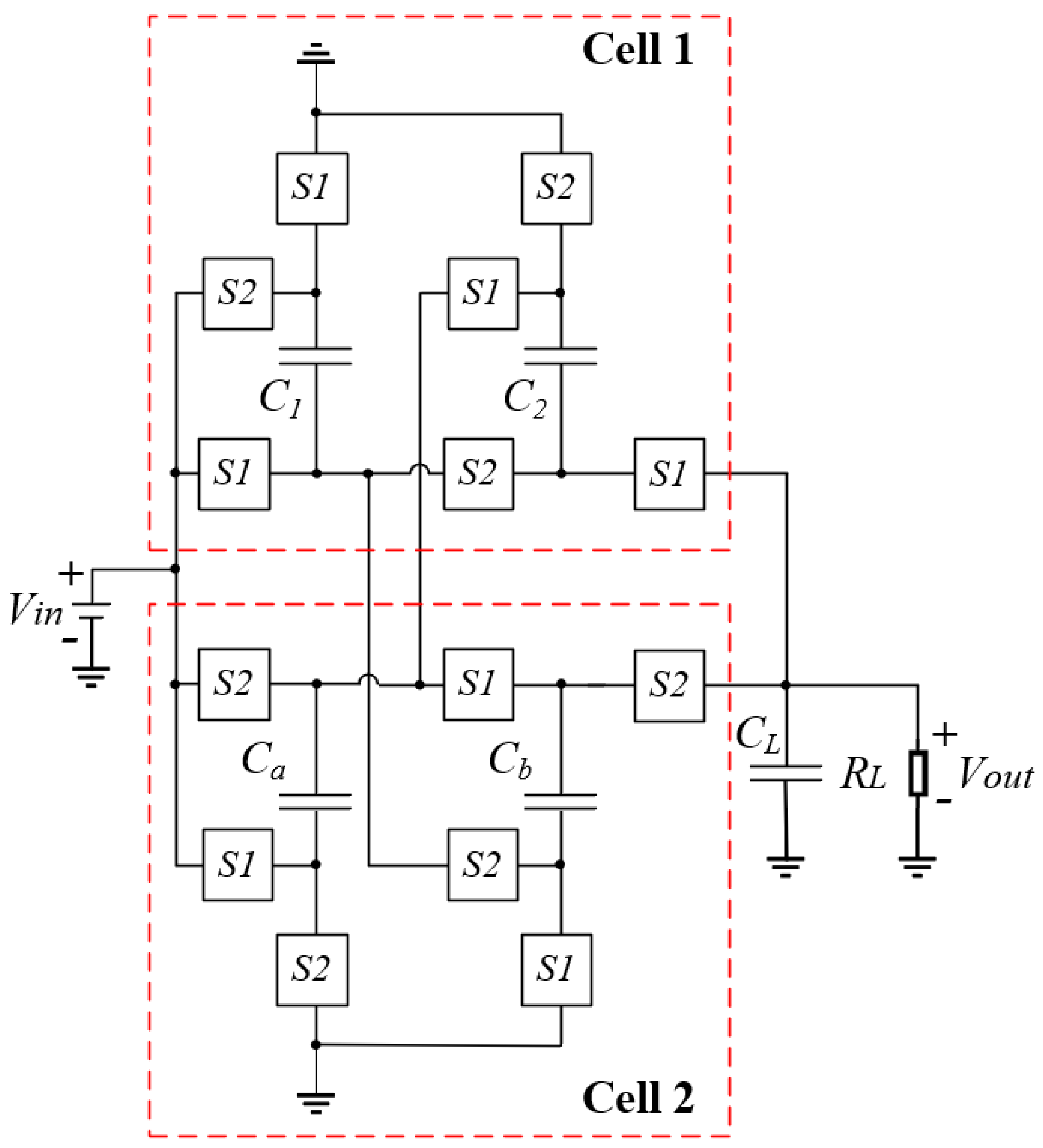
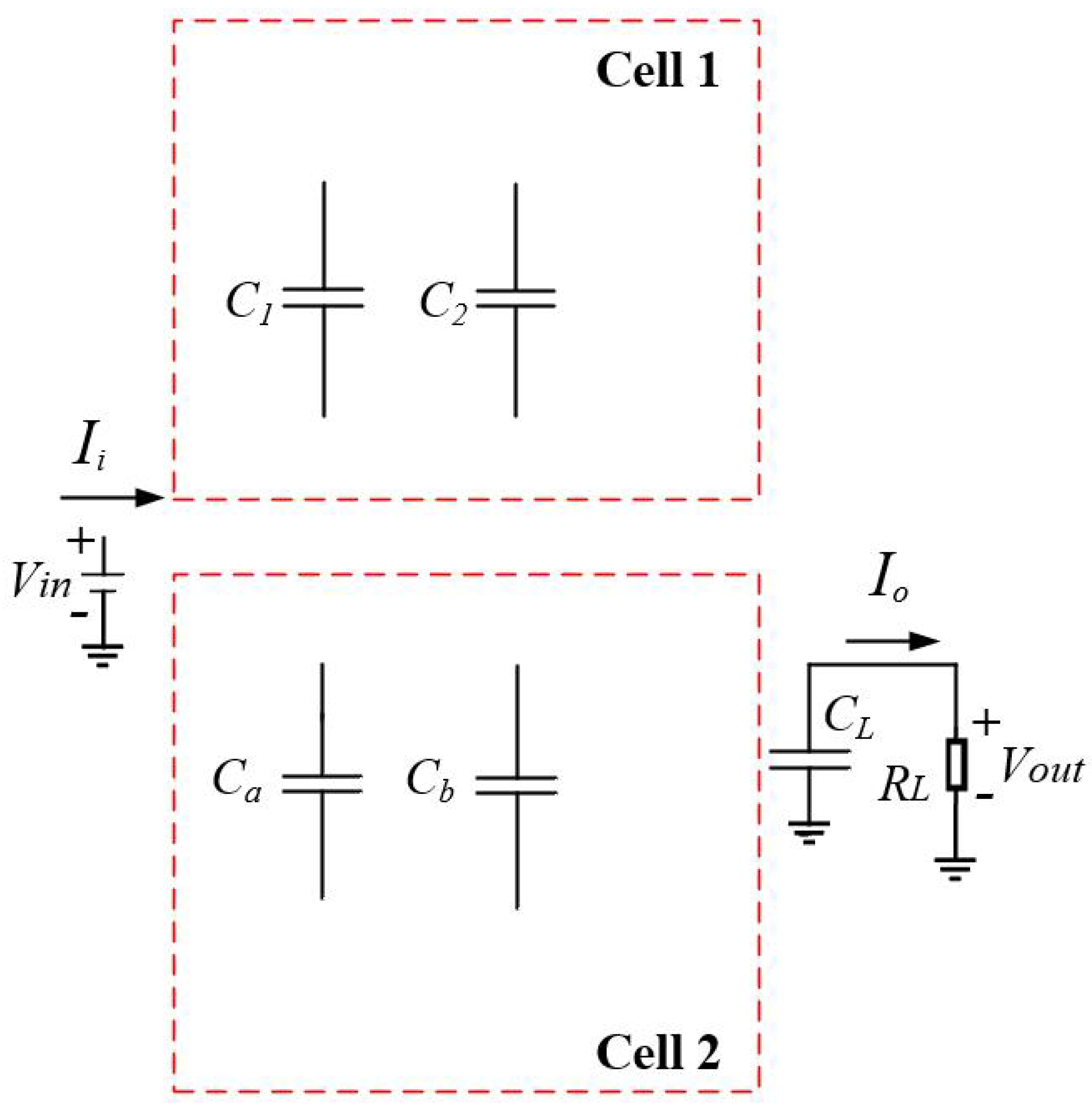
2. Circuit Configuration

Figure 1 shows the cross-connected Fibonacci switched capacitor converter (CCFSCC) with its four times step-up mode, where V i n is the average input voltage, V o u t is the average output voltage, S 1 and S 2 are semiconductor switches, C i ( i = 1 , 2 , a , b ) are flying capacitors, R L is the load resistor, and C L is the output capacitor [27]. The CCFSCC consists of two cross-connected FSCCs (Cells 1 and 2). It is operated by turning on and off switches ( S 1 and S 2 ). They are controlled by the pulse width modulation (PWM) signals ( Φ 1 and Φ 1 ) with its dead-time, as described in Figure 2, where S 1 and S 2 are for State-1 and State-2, T is the operation period during one cycle, and D is its duty ratio. In terms of the duty ratio D, the CCFSCC features a symmetric construction. Therefore, the duty ratio D is designated as 50%.
Figure 3 describes instantaneous equivalent circuits in steady-state at State-1 and State-2, where R o n s are the on-resistors of the switches and I i and I o are the input and output currents, respectively. In steady-state, if there is no power loss, capacitors C 1 and C a are charged up to the input voltage V i n . Then, each of them charges capacitors C 2 and C b up to 2 V i n . Finally, these capacitors charge the output capacitor C L up to 4 V i n . In the next section, the CCFSCC is theoretically analyzed.

3. Theoretical Analysis

3.1. Voltage Gain Function

In this subsection, an analysis is conducted with some the assumptions that the dead time is zero and the output capacitor has no influence on the output voltage, and this analysis focuses on the CCFSCC in steady state [26,27].
By using KCL and KVL in the instantaneous equivalent circuit at State-1 in Figure 3a, Equations (1)–(3) are derived, where R is the resistance of on-resistors, C f is the capacitance of flying capacitors, and V C x ( x = 1 , 2 , a , b ) are the voltages of the capacitors [26,27].
C f d V C a d t = C f d V C b d t + C f d V C 2 d t .
V i n R C f d V C a d t + R C f d V C 1 d t + V C 1 + R C f d V C 1 d t = 0 .
2 R C f d V C b d t V C b 2 R C f d V C 2 d t V C 2 + V o = 0 .
Considering the symmetric structure of the CFSCC and using Equation (3), the output voltage is obtained as Equation (4). From Equation (4), the output voltage can be approximately rewritten as Equation (5), where V C x , m i n and V C x , m a x ( x = 1 , 2 , b ) are the minimum and maximum voltages of the capacitors. If this approximation is not conducted, all of the minimum and maximum voltages of the capacitors should be derived such as in the method in [32,33,34].
V o = V C 2 + V C b .
V o V C 2 , m i n + V C 2 , m a x 2 + V C b , m i n + V C b , m a x 2 2 V C 1 , m i n + V C 1 , m a x .
By using Equation (2), the relation of C 1 voltage and input source during State-1 can be expressed as given in Equation (6).
V C 1 t = V C 1 , m i n V i n e 1 3 R C f t + V i n .
From Equation (6), the maximum voltage of C 1 at t = T 2 is given by Equation (7).
V C 1 , m a x = V C 1 , m i n V i n e 1 3 R C f T 2 + V i n .
From the symmetric structure of the CFSCC, the average output current can be rewritten as Equation (8).
I o T = V o R L T = C f V C 1 , m a x V C 1 , m i n .
Solving a linear equation consisting of Equations (7) and (8), minimum voltage of C 1 is obtained, as presented in Equation (9).
V C 1 , m i n = T R L C f K 1 + V i n ,
where K = e 1 3 R C f T 2 .
By substituting the maximum and minimum voltages of C 1 and Equations (7) and (9) into Equation (5) and rearranging the result, the voltage gain function, g, of the CFSCC is obtained, as given in Equation (10).
g = V o V i n = 4 4 T R L C f K 1 2 T R L C f + 1 .

3.2. Optimization

For efficient design and desirable operation of the CCFSCC, it is required to select proper values of circuit parts such as capacitances of its capacitors and operation frequency. In this subsection, an optimization approach for appropriate values of circuit parts is conducted based on the voltage gain function presented in Equation (10).
The optimization is implemented with the default set-up shown in Table 1. Fixing the default setting, the proper value is decided by tuning the target parameter.

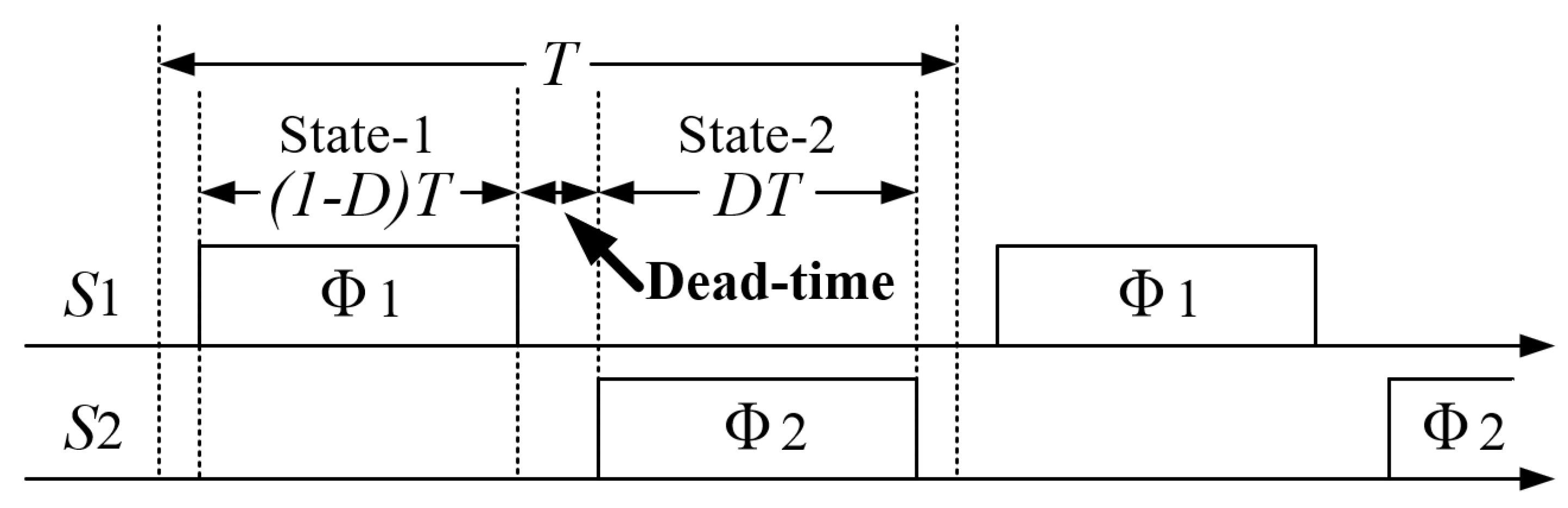
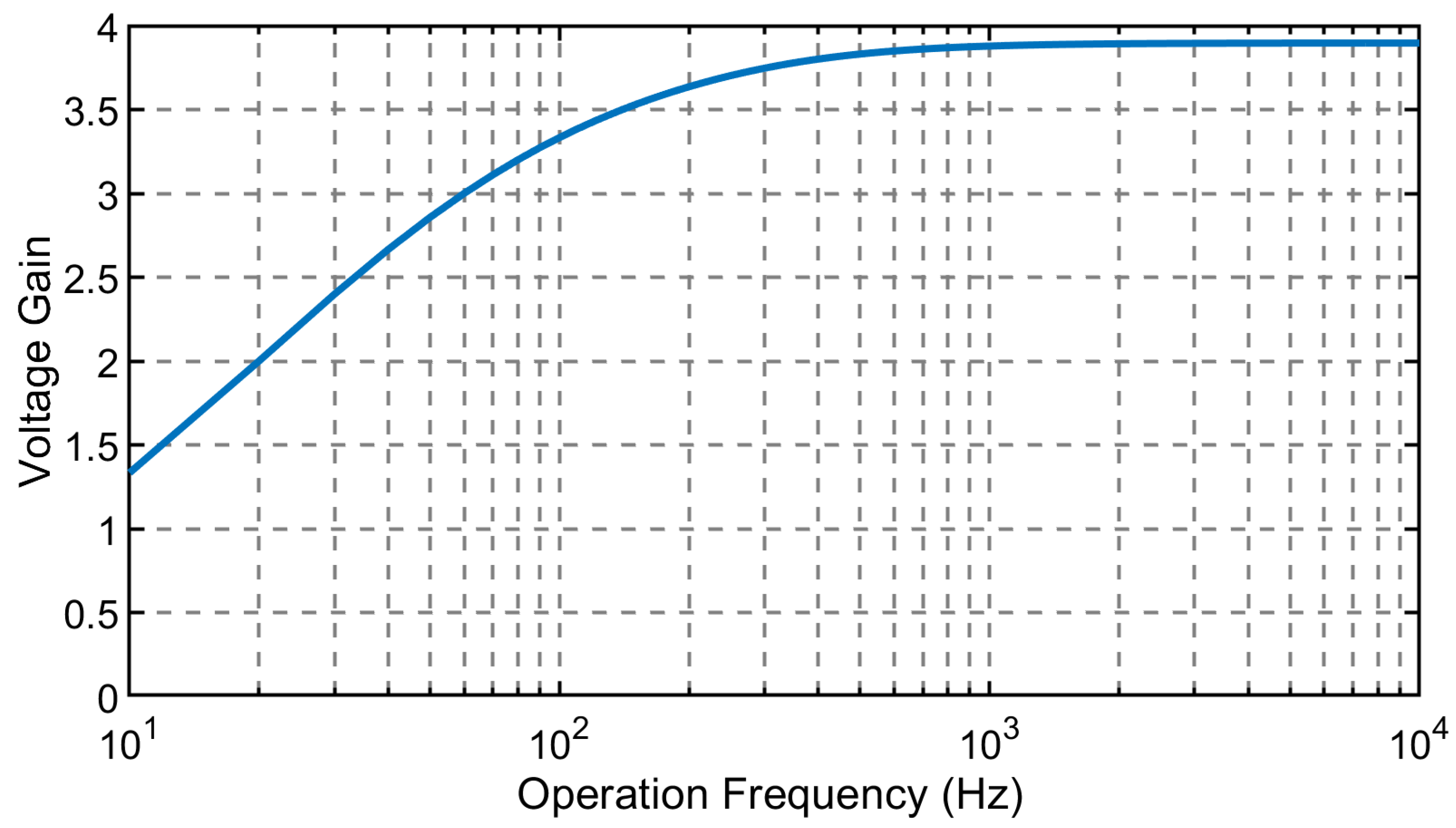
3.2.1. Operation Frequency

When an operation frequency for a power converter is selected, circuit designers should consider the influence on the voltage gain as well as charging time constants of flying capacitors. In terms of the time constant, the flying capacitors can be charged up to over 95% of their fully-charged voltage as long as the operation period is over three times the charging time constant.
In the case of the CCFSCC, the boundary of the time constant can be set up to 9 R o n C f , because all flying capacitors have the same charging time constants according to Equation (5).
The voltage gain regulations at different operation frequencies is shown in Figure 4, where the range of the frequency is from 10 Hz to 10 kHz. In this case with the default set-up, selecting the frequency over 1 kHz makes the voltage gain on a stable condition. The higher limit of the frequency should be selected by falling and rising times of the switches.

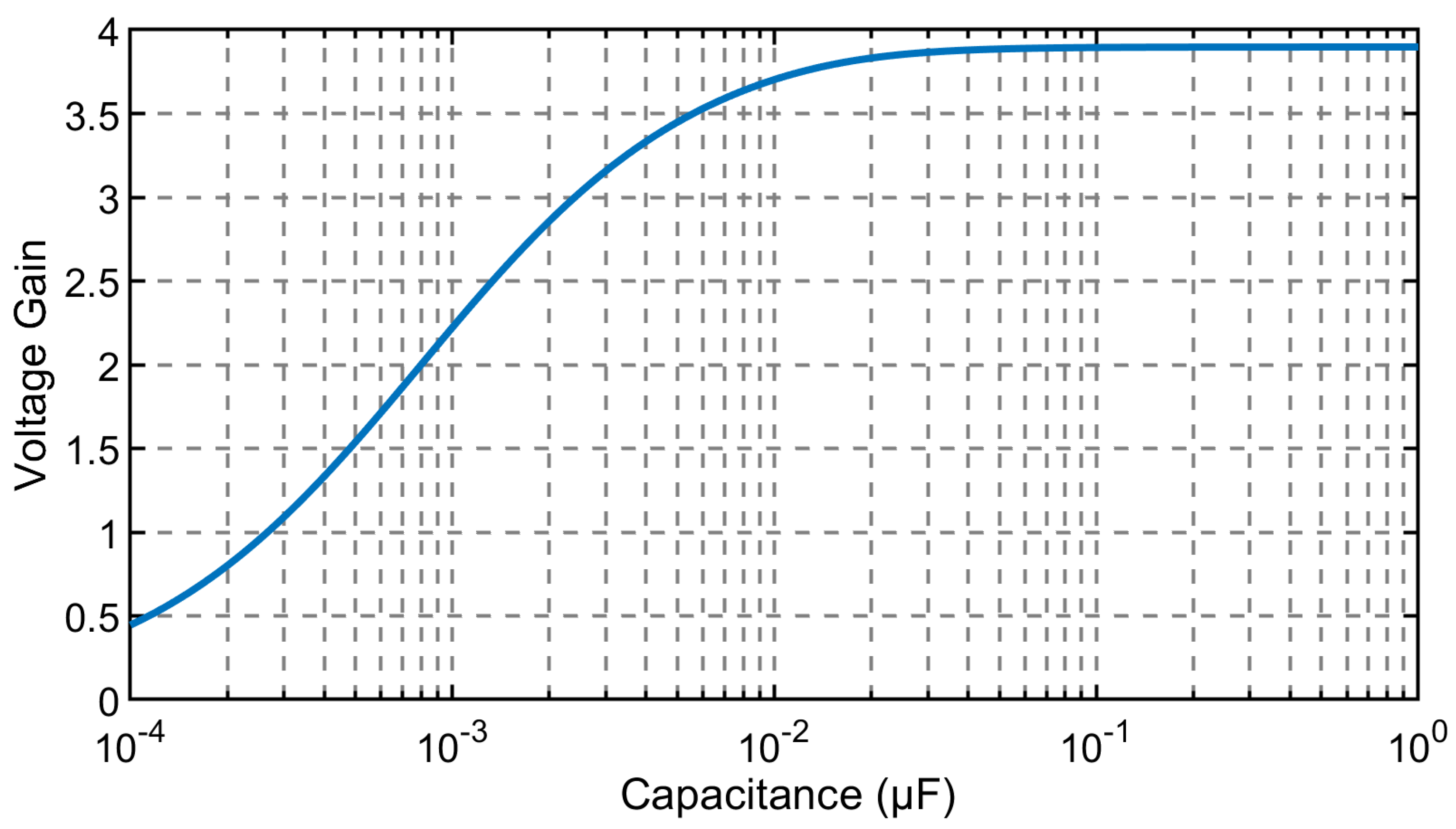
3.2.2. Flying Capacitors Capacitance

The voltage gain function provides only the lower limit of the capacitance. Its higher limit should be considered regarding the operation frequency because of its impact on the charging time constant.
In the example case with the default set-up, the voltage gain regulations at different capacitances from 0.1 nF to 1 μ F is illustrated in Figure 5. This figure states that the voltage gains with the capacitances higher than 0.1 μ F are stable. To maintain 95% of the fully charged voltage, the capacitance is required to be lower than T 18 R o n . With these conditions, the appropriate capacitance range can be expressed as follows
0.1 μ F < C f < 20.2 μ F .

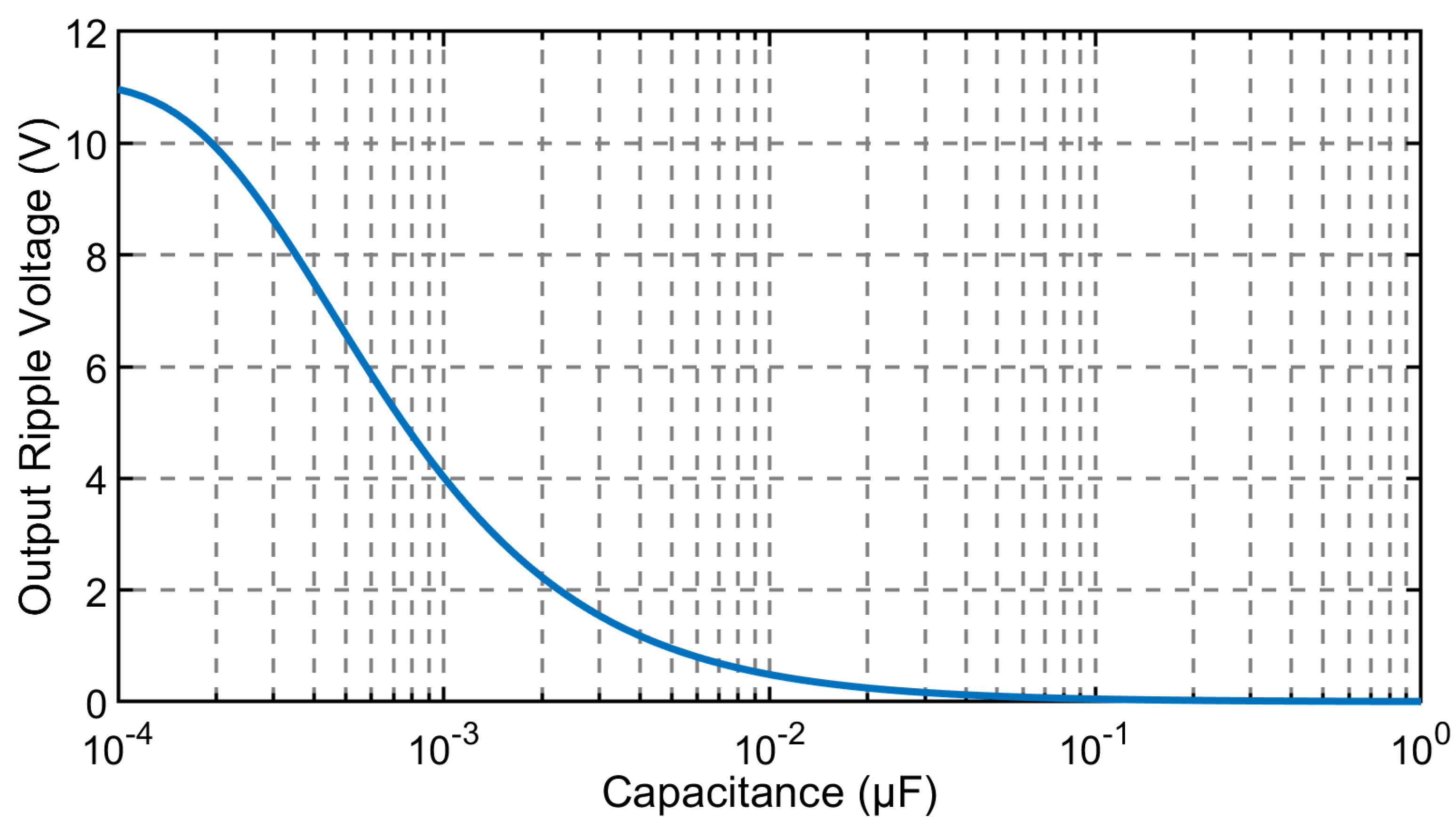
3.2.3. Output Capacitor Capacitance

The output capacitor of a practical CCFSCC is charged during State-1 and State-2 and discharged during dead-times. This operation causes the output ripple voltage. The instantaneous circuit during the dead-times is shown in Figure 6. The output ripple voltage is the difference between the maximum and minimum output voltages. Therefore, deriving the output ripple voltage is implemented with an assumption that the maximum output voltage of the CCFSCC is approximately g V i n . From this assumption, the output ripple voltage, V o , r i p p l e , can be expressed as Equation (12).
V o , r i p p l e = V o , m a x V o , m i n = g V i n V o , m i n = g V i n g V i n e T d e a d R L C L ,
where V o , m i n is derived from the instantaneous circuit in Figure 6.
Using the ripple voltage of Equation (12) and the default set-up, the output ripple voltage at different capacitances of the output capacitor (from 0.1 nF to 1 μ F) is shown in Figure 7. The waveform in Figure 7 can provide the lower limit of the output capacitor capacitance. The range of the output capacitor capacitance can be expressed as follows
C f > 0.1 μ F .

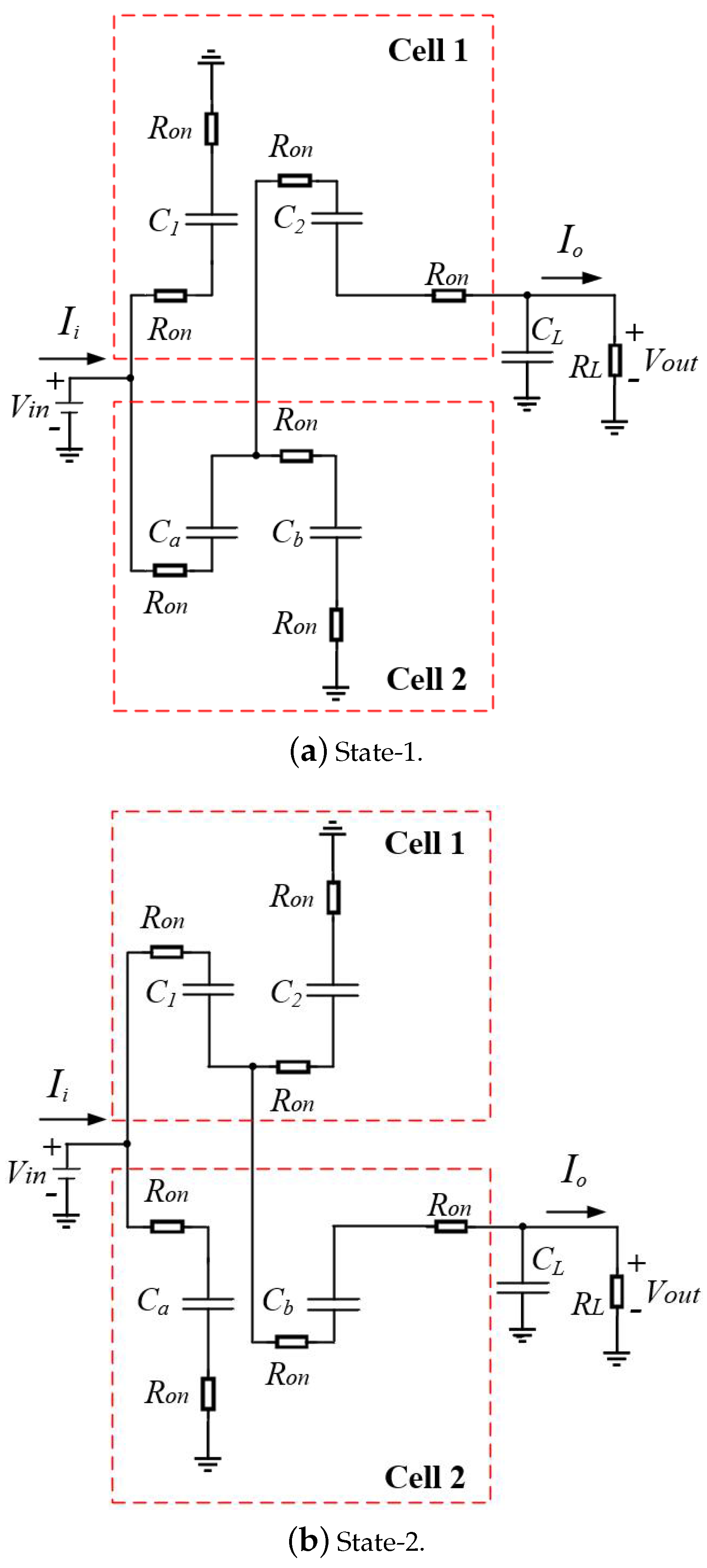
3.3. Power Stage Transfer Function

Generally, stability of a power converter is judged by deriving and analyzing its power stage transfer function [35,36,37]. The power stage transfer function of the CCFSCC is obtained in this subsection by directly modeling it in z-domain. This modeling is conducted with consideration of the dead time.
During State-1, the flying capacitors ( C 1 and C b ) and the output capacitor C L are charged. The others are discharged. The voltages across C 1 and C b are approximately V i n and 2 V i n , and the voltage across C L is the same as the output voltage, V o . Therefore, the charged and discharged charges ( Q c h a r and Q d i s ) at ( n 1 ) T can be derived as Equations (14) and (15), respectively.
Q c h a r ( n 1 ) T = 3 C f V i n ( n 1 ) T + C L V o ( n 1 ) T .
Q d i s ( n 1 ) T = 2 C f V i n ( n 1 ) T .
During the dead-time, the discharged charge ( Q d i s , d e a d ) is also obtained, as given in Equation (16).
Q d i s , d e a d n T = C L V o n T .
In agreement with the charge conservation law, the net current on the flying capacitors should be the same as the output current during one operating period T. This can be expressed as Equation (17).
C f V i n ( n 1 ) T + C L V o ( n 1 ) T C L V o n T T 2 = V o ( n 1 ) T R L + V o T R L .
By rearranging and z-transforming Equation (14), the power stage transfer function is given by Equation (18).
V o V i n = C f C L + T t o a l 2 R L z C L T t o a l 2 L C L + T t o a l 2 R L .
Equation (18) has only one pole at C L T t o a l 2 L C L + T t o a l 2 R L , and this leads the CCFSCC to stably operate unless a low-frequency pole is added to its control loop [38,39,40].

4. Simulation, Experiment and Comparison

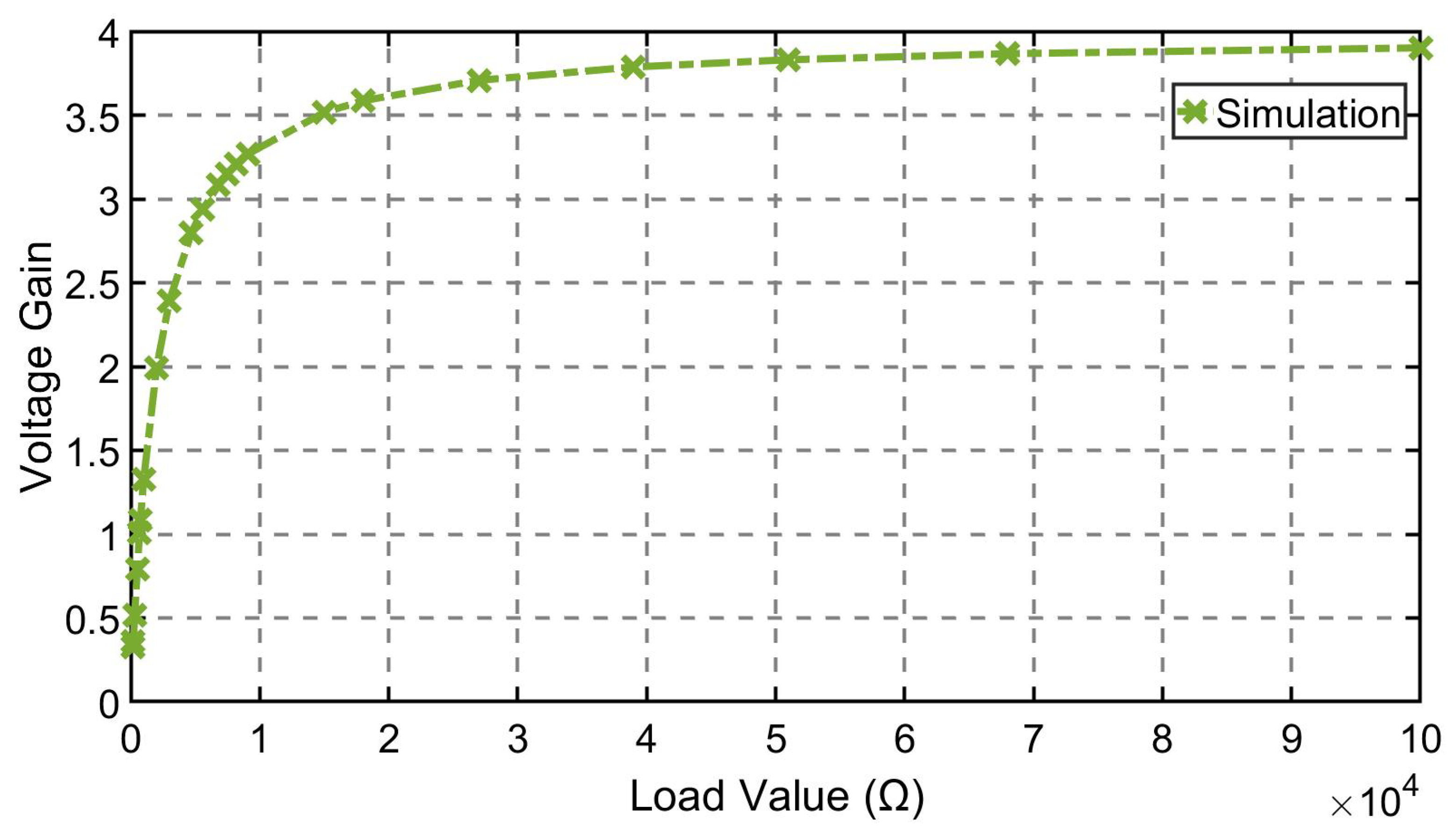
4.1. Simulation Result

To confirm the reliability of the proposed model, the CCFSCC was simulated through the SPICE simulation with the given parameters in Table 2. In this simulation, ideal capacitors and resistors without parasitic components were used. Figure 8 shows the simulated voltage gain regulations at different load register values.

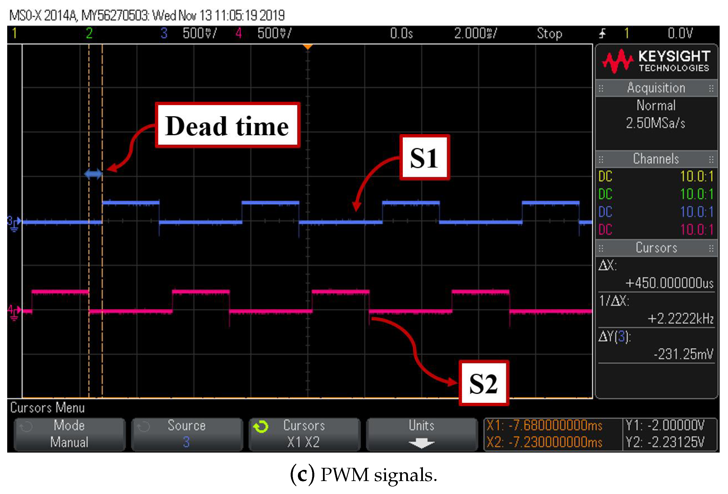
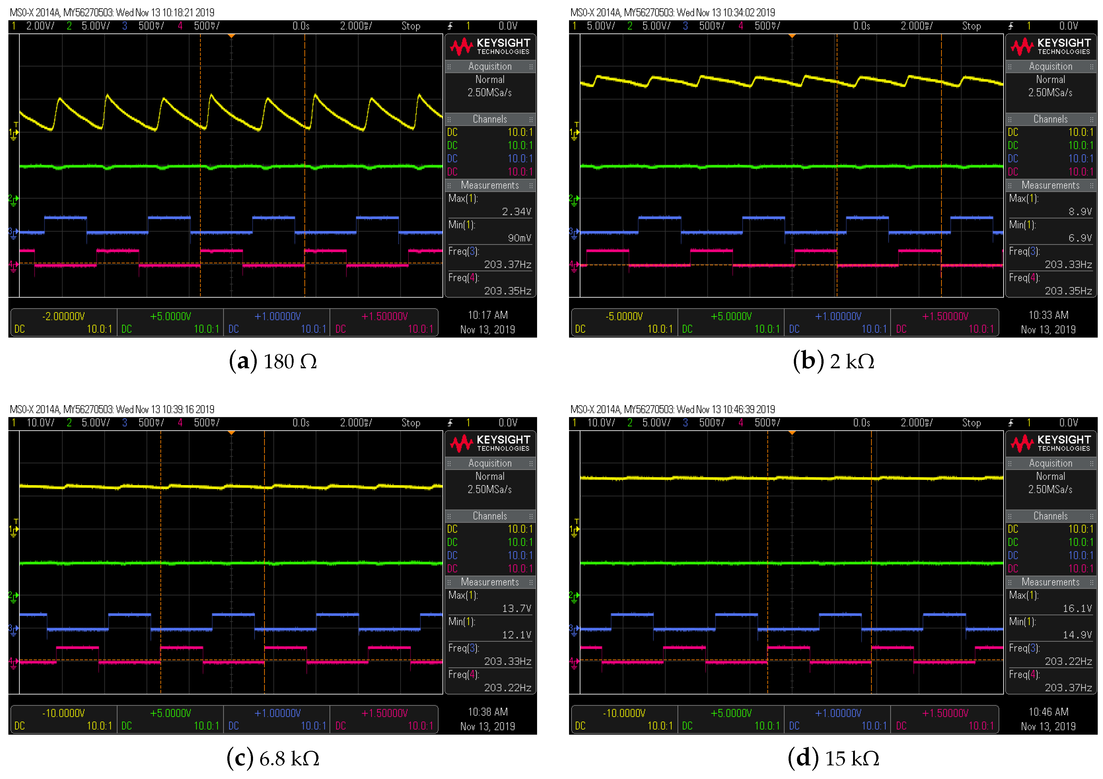
4.2. Experimental Result

To affirm the accuracy of the proposed model, an experimental test was implemented with the circuit components in Table 3 and the experimental set-up shown in Figure 9a. In Table 3, T o n is the on-time of the switches and T d e a d is the dead-time. Figure 9b shows the prototype configuration of the CCFSCC. The CCFSCC is operated by the PWM signals, as shown in Figure 9c. Figure A1 describes the measured output voltages with the input voltage and the PWM signals at different load values (from 180 Ω to 15 k Ω ). In Figure A1, yellow signals are output voltages, green signals are input voltages, and other signals are PWM signals.

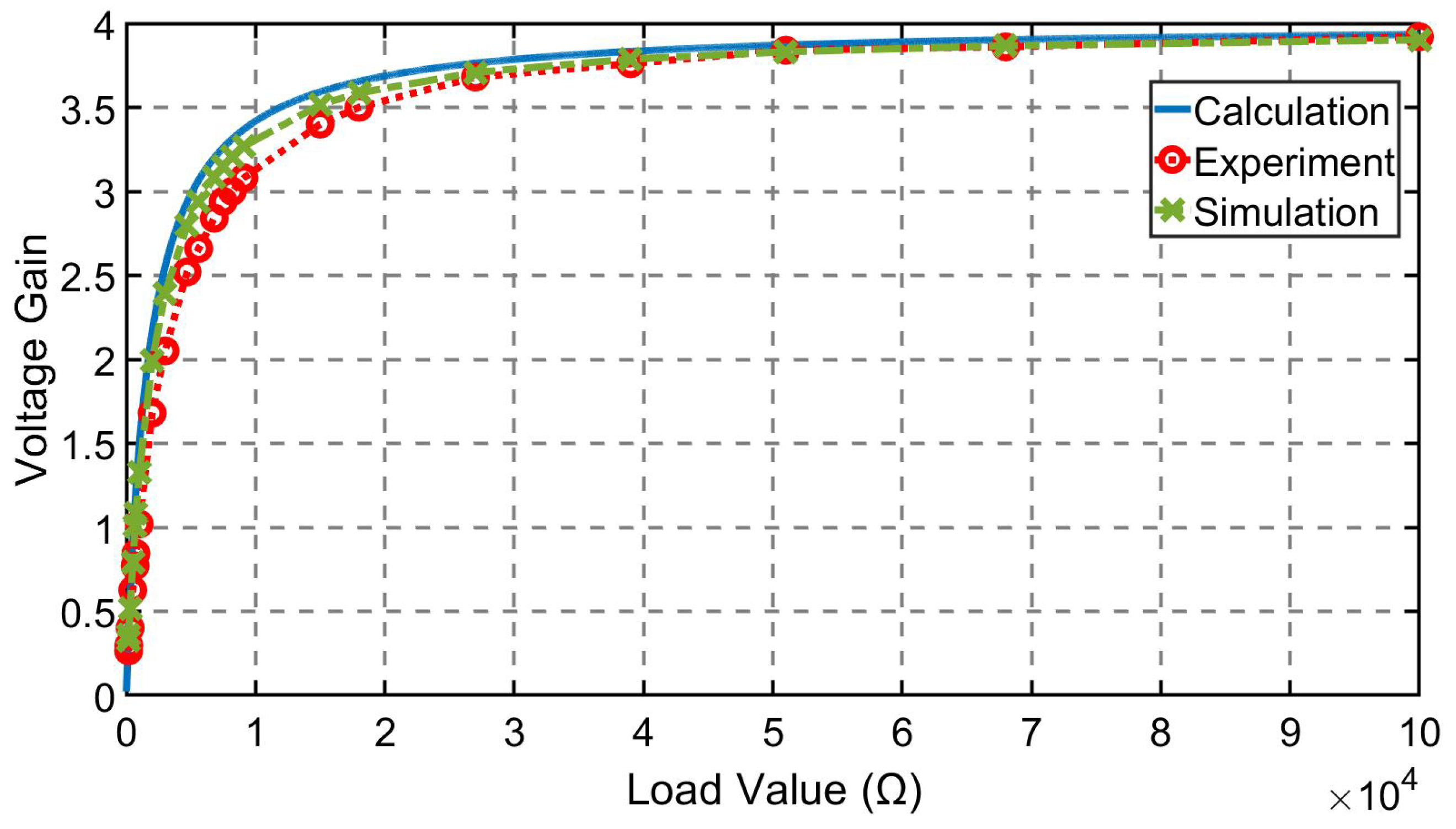
4.3. Comparison of Calculation, Simulation and Experimental Results

Figure 10 illustrates the calculated, simulated, and experimental voltage gain regulations at different load values. The average errors between the calculated and simulated voltage gains is 6.9% on average. The difference of average errors between the proposed approach and the experiments is 9%, the details of which are as follows: 30.39% (the calculations and the experiments) and 21.39% (the simulations and the experiments) on average. However, the curve of the calculated voltage gains follows closely the simulated and experimental ones as the load values increase. Additionally, the average absolute errors of the voltage gains are as follows: 0.42 (the calculations and the experiments), 0.33 (the simulations and the experiments), and 0.09 (the calculations and the simulations).

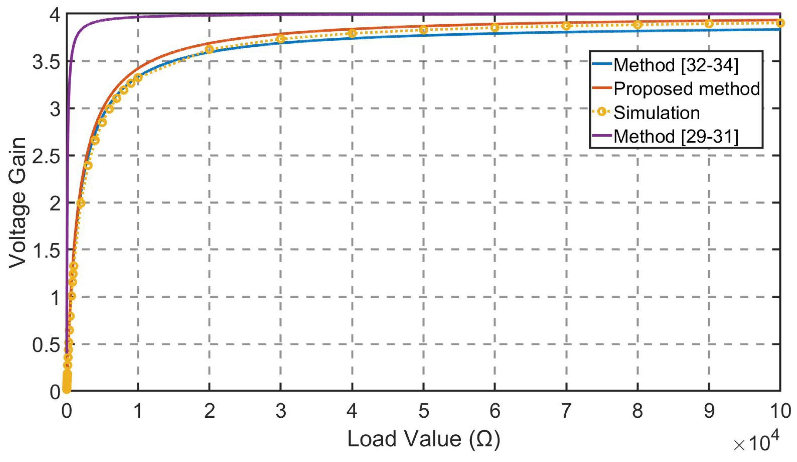
4.4. Comparison with Existing Methods

Figure 11 describes the comparison of voltage gains by the proposed approach and existing methods in [29,30,31,32,33,34] at different load values. These are derived with the parameters in Table 2.
In the slow and fast switching limit model, an SCC is modeled. The duty ratio is fixed 50%, resistors of switches are neglected, and variations in charging and discharging voltages of capacitors are also neglected [29,30,31]. Unlike the conventional method, the proposed method can reflect the influence on the gain function by the duty ratio when maximum and minimum voltages of capacitors are derived. When the relation of the operation frequency, capacitors, and switches is modeled, the method in [29,30,31] neglects on-resistors of switches (slow switching limit) and considers the capacitors as voltage sources (fast switching limit). These characteristics decrease the accuracy of the voltage gain, as shown in Figure 11. However, in the proposed method, these parameters are examined through all analysis processes, as explained in Section 3.1. These differences from the existing method can increase the modeling accuracy of the proposed method.
If the CCFSCC is analyzed by using the given method in [32,33,34], the voltages of all of the capacitors need to be derived. This can improve the reliability of the voltage gains at load values under 2 k Ω , as described in Figure 11, but requires complex calculations as the number of circuit components rises to generate higher output voltages. Differently from this method, the proposed method approximates the voltages of capacitors, as formulated in Equation (5). This can reduce the amount of calculations.

5. Conclusions

In this paper, we propose an analytical method to analyze the CCFSCC in steady state condition. From the proposed modeling, the voltage gain function of the CCFSCC is derived to provide a guidance for selecting the circuit parameters such as the operation frequency and the capacitances of the flying and output capacitors. To verify the proposed method, the outcomes were compared with the simulated and experimental results at different load values. The absolute error between the calculations and the simulations is under 0.1 on average. This comparison shows that the proposed analytical method can be considered as a guidance to design hardware for the CCFSCC.
In a future study, hardware for the CCFSCC will be designed by selecting proper circuit components based on the proposed guidance, which can prove the reliability of the proposed analytical method. Additionally, analyzing and designing different types of SCCs with the proposed method will be implemented, which can prove generality and versatility of the proposed method.

Author Contributions

Conceptualization, Q.S. and K.E.; Methodology, W.D. and H.B.; Project administration, K.E.; Writing—original draft, W.D.; Writing—review & editing, H.B., Q.S. and K.E. All authors have read and agreed to the published version of the manuscript.

Funding

This research received no external funding.

Conflicts of Interest

The authors declare no conflict of interest.

Appendix A

Figure A1 illustrates the measured input and output voltages and PWM signals.
Figure A1. Measured output voltages at different load values from 180 Ω to 15 k Ω .
Energies 13 00431 g0a1

References

  1. Htet, K.O.; Fan, H.; Heidari, H. Switched Capacitor DC-DC Converter for Miniaturised Wearable Systems. In Proceedings of the 2018 IEEE International Symposium on Circuits and Systems (ISCAS), Florence, Italy, 27–30 May 2018; pp. 1–5. [Google Scholar]
  2. Kilani, D.; Mohammad, B.; Alhawari, M.; Saleh, H.; Ismail, M. A Dual-Output Switched Capacitor DC–DC Buck Converter Using Adaptive Time Multiplexing Technique in 65-nm CMOS. IEEE Trans. Circuits Syst. I Regul. Pap. 2018, 65, 4007–4016. [Google Scholar] [CrossRef]
  3. Grasso, A.D.; Palumbo, G.; Pennisi, S. Switched-Capacitor Power Management Integrated Circuit for Autonomous Internet of Things Node. IEEE Trans. Circuits Syst. II Express Briefs 2018, 65, 1455–1459. [Google Scholar] [CrossRef]
  4. Shah, N.; Lajevardi, P.; Wojciechowski, K.; Lang, C.; Murmann, B. An Energy Harvester Using Image Sensor Pixels With Cold Start and Over 96% MPPT Efficiency. IEEE Solid State Circuits Lett. 2019, 2, 207–210. [Google Scholar] [CrossRef]
  5. Wu, X.; Shi, Y.; Jeloka, S.; Yang, K.; Lee, I.; Lee, Y.; Sylvester, D.; Blaauw, D. A 20-pW Discontinuous Switched-Capacitor Energy Harvester for Smart Sensor Applications. IEEE J. Solid-State Circuits 2017, 52, 972–984. [Google Scholar] [CrossRef]
  6. Alhawari, M.; Kilani, D.; Mohammad, B.; Saleh, H.; Ismail, M. An efficient thermal energy harvesting and power management for μWatt wearable BioChips. In Proceedings of the 2016 IEEE International Symposium on Circuits and Systems (ISCAS), Montreal, QC, Canada, 22–25 May 2016; pp. 2258–2261. [Google Scholar]
  7. Liu, X.; Ravichandran, K.; Sánchez-Sinencio, E. A Switched Capacitor Energy Harvester Based on a Single-Cycle Criterion for MPPT to Eliminate Storage Capacitor. IEEE Trans. Circuits Syst. I Regul. Pap. 2018, 65, 793–803. [Google Scholar] [CrossRef]
  8. Nielsen-Lónn, M.; Angelov, P.; Wikner, J.J.; Alvandpour, A. Self-oscillating multilevel switched-capacitor DC/DC converter for energy harvesting. In Proceedings of the 2017 IEEE Nordic Circuits and Systems Conference (NORCAS): NORCHIP and International Symposium of System-on-Chip (SoC), Linkoping, Sweden, 23–25 October 2017; pp. 1–5. [Google Scholar]
  9. Mohey, A.M.; Ibrahim, S.A.; Hafez, I.M.; Kim, H. Design Optimization for Low-Power Reconfigurable Switched-Capacitor DC-DC Voltage Converter. IEEE Trans. Circuits Syst. I Regul. Pap. 2019, 66, 4079–4092. [Google Scholar] [CrossRef]
  10. Lee, H.; Jang, E.; Saif, H.; Lee, Y.; Kim, M.; Khan, M.B.; Lee, Y. A Sub-nW Fully Integrated Switched-Capacitor Energy Harvester for Implantable Applications. In Proceedings of the IEEE 44th European Solid State Circuits Conference (ESSCIRC), Dresden, Germany, 3–6 September 2018; pp. 50–53. [Google Scholar]
  11. Forouzesh, M.; Siwakoti, Y.P.; Gorji, S.A.; Blaabjerg, F.; Lehman, B. Step-Up DC–DC Converters: A Comprehensive Review of Voltage-Boosting Techniques, Topologies, and Applications. IEEE Trans. Power Electron. 2017, 32, 9143–9178. [Google Scholar] [CrossRef]
  12. Dickson, J.F. On-chip high-voltage generation in mnos integrated circuits using an improved voltage multiplier technique. IEEE J. Solid-State Circuits 1976, 32, 374–378. [Google Scholar] [CrossRef]
  13. Mahmoud, A.; Alhawari, M.; Mohammad, B.; Saleh, H.; Ismail, M. A Gain-Controlled, Low-Leakage Dickson Charge Pump for Energy-Harvesting Applications. IEEE Trans. VLSI Syst. 2019, 27, 1114–1123. [Google Scholar] [CrossRef]
  14. Schaef, C.; Stauth, J.T. A Highly Integrated Series–Parallel Switched-Capacitor Converter With 12 V Input and Quasi-Resonant Voltage-Mode Regulation. IEEE J. Emerg. Sel. Top Power Electron. 2018, 6, 456–464. [Google Scholar] [CrossRef]
  15. Beck, Y.; Singer, S. General transposed series-parallel switched capacitor converter topologies. In Proceedings of the 2017 IEEE AFRICON, Cape Town, South Africa, 18–20 September 2017; pp. 1351–1356. [Google Scholar]
  16. Abraham, C.; Jose, B.R.; Mathew, J.; Evzelman, M. Modelling, simulation and experimental investigation of a new two input, series-parallel switched capacitor converter. IET Power Electron. 2017, 10, 368–376. [Google Scholar] [CrossRef]
  17. Cao, D.; Peng, F.Z. Zero-current-switching multilevel modular switched-capacitor DC–DC converter. In Proceedings of the IEEE Energy Conversion Congress and Exposition (ECCE), San Jose, CA, USA, 20–24 September 2009; pp. 3516–3522. [Google Scholar]
  18. Cao, D.; Jiang, S.; Peng, F.Z. Optimal design of multilevel modular switched-capacitor DC-DC converter. In Proceedings of the IEEE Energy Conversion Congress and Exposition, Phoenix, AZ, USA, 17–22 September 2011; pp. 537–544. [Google Scholar]
  19. Cao, D.; Peng, F.Z. Multiphase multilevel modular DC–DC converter for high-current high-gain TEG application. IEEE Trans. Ind. Appl. 2011, 47, 1400–1408. [Google Scholar]
  20. Zanwar, M.; Sen, S. Design of CMOS programmable output binary and fibonacci switched capacitor step-down DC-DC converter. In Proceedings of the 2016 International Conference on VLSI Systems, Architectures, Technology and Applications (VLSI-SATA), Bangalore, India, 10–12 January 2016; pp. 1–6. [Google Scholar]
  21. Subburaj, V.; Jena, D.; Kumar, R.; Deshmukh, A.V.; Nayak, B.; Bansal, H. Design of series, Fi=Fi-1+Fi-3 for the denominators (1, 2,.. 6) of switched capacitor converter. In Proceedings of the 2016 IEEE 1st International Conference on Power Electronics, Intelligent Control and Energy Systems (ICPEICES), Delhi, India, 4–6 July 2016; pp. 1–5. [Google Scholar]
  22. Junussov, A.; Ruderman, A. Analysis of a reconfigurable Fibonacci switched capacitor converter with a multiphase balanced switching. In Proceedings of the 2015 IEEE 5th International Conference on Power Engineering, Energy and Electrical Drives (POWERENG), Riga, Latvia, 11–13 May 2015; pp. 164–169. [Google Scholar]
  23. Sanders, S.R.; Alon, E.; Le, H.; Seeman, M.D.; John, M.; Ng, V.W. The Road to Fully Integrated DC–DC Conversion via the Switched-Capacitor Approach. IEEE Trans. Power Electron. 2013, 28, 4146–4155. [Google Scholar] [CrossRef]
  24. Seeman, M.D.; Ng, V.W.; Le, H.; John, M.; Alon, E.; Sanders, S.R. A comparative analysis of Switched-Capacitor and inductor-based DC-DC conversion technologies. In Proceedings of the 2010 IEEE 12th Workshop on Control and Modeling for Power Electronics (COMPEL), Boulder, CO, USA, 28–30 June 2010; pp. 1–7. [Google Scholar]
  25. Eguchi, K.; Hirata, S.; Shimoji, M.; Zhu, H. Design of a Step-Up/Step-Down k (=2,3,...)-Fibonacci DC-DC Converter Designed by Switched-Capacitor Techniques. In Proceedings of the 2012 Fifth International Conference on Intelligent Networks and Intelligent Systems, Tianjin, China, 1–3 November 2012; pp. 170–173. [Google Scholar]
  26. Do, W.; Fujisaki, H.; Asadi, F.; Eguchi, K. A Cross-Connected Charge Pump for Energy Harvesting Applications. IJICIC 2019, 15, 969–982. [Google Scholar]
  27. Rubpongse, R.; Asadi, F.; Do, W.; Eguchi, K. Experiment of a High Voltage Gain Switched Capacitor DC-DC Converter Based on a Cross-Connected Fibonacci-Type Converter. ICIC Express Lett. 2019, 13, 393–400. [Google Scholar]
  28. Eguchi, K.; Julsereewong, P.; Julsereewong, A.; Fujimoto, K.; Sasaki, H. A Dickson-type adder/subtractor DC-DC converter realizing step-up/step-down conversion. IJICIC 2013, 9, 123–138. [Google Scholar]
  29. Seeman, M.D.; Sanders, S.R. Analysis and Optimization of Switched-Capacitor DC–DC Converters. IEEE Trans. Power Electron. 2008, 23, 841–851. [Google Scholar] [CrossRef]
  30. Vos, J.D.; Flandre, D.; Bol, D. A Sizing Methodology for On-Chip Switched-Capacitor DC/DC Converters. IEEE Trans. Circuits Syst. I Regul. Pap. 2014, 61, 1597–1606. [Google Scholar] [CrossRef]
  31. Ng, V.W.; Sanders, S.R. A High-Efficiency Wide-Input-Voltage Range Switched Capacitor Point-of-Load DC–DC Converter. IEEE Trans. Power Electron. 2013, 28, 4335–4341. [Google Scholar] [CrossRef]
  32. Wu, B.; Li, S.; Smedley, K.M.; Singer, S. Analysis of High-Power Switched-Capacitor Converter Regulation Based on Charge-Balance Transient-Calculation Method. IEEE Trans. Power Electron. 2016, 31, 3482–3494. [Google Scholar] [CrossRef]
  33. Yang, L.; Wu, B.; Tong, X.; Smedley, K.M.; Li, G. Dynamic Capacitor Ampere-Second Balance Transient Calculation Modeling Method for Switched-Capacitor Converters. IEEE Trans. Power Electron. 2018, 33, 8916–8926. [Google Scholar] [CrossRef]
  34. Wu, B.; Yang, L.; Zhang, X.; Smedley, K.M.; Li, G. Modeling and Analysis of Variable Frequency One-Cycle Control on High-Power Switched-Capacitor Converters. IEEE Trans. Power Electron. 2018, 33, 5465–5475. [Google Scholar] [CrossRef]
  35. Wester, G.W.; Middlebrook, R.D. Low-Frequency Characterization of Switched dc-dc Converters. IEEE Trans. Aerosp. Electron. Syst. 1973, AES-9, 376–385. [Google Scholar] [CrossRef] [Green Version]
  36. Solero, L.; Lidozzi, A.; Pomilio, J.A. Design of multiple-input power converter for hybrid vehicles. IEEE Trans. Power Electron. 2005, 31, 1007–1016. [Google Scholar] [CrossRef]
  37. Sankaranarayanan, V.; Shirazi, M.; Gao, Y.; Ghosh, A.; Erickson, R.W.; Maksimovic, D. Controller Hardware-in-the-Loop Validation of a Modular Control Architecture for a Composite DC-DC Converter. In Proceedings of the 2019 20th Workshop on Control and Modeling for Power Electronics (COMPEL), Toronto, ON, Canada, 17–20 June 2019; pp. 1–7. [Google Scholar]
  38. Su, L.; Ma, D.; Brokaw, A.P. Design and Analysis of Monolithic Step-Down SC Power Converter With Subthreshold DPWM Control for Self-Powered Wireless Sensors. IEEE Trans. Circuits Syst. I Regul. Pap. 2010, 57, 280–290. [Google Scholar]
  39. Su, L.; Ma, D.; Brokaw, A.P. A monolithic step-down SC power converter with frequency-programmable subthreshold z-domain DPWM control for ultra-low power microsystems. In Proceedings of the ESSCIRC 2008—34th European Solid-State Circuits Conference, Edinburgh, UK, 15–19 September 2008; pp. 58–61. [Google Scholar]
  40. Zheng, C.; Su, L.; Ma, D. A Systematic USFG Design Approach for Integrated Reconfigurable Switched-Capacitor Power Converters. IEEE Trans. Circuits Syst. I Regul. Pap. 2011, 58, 2790–2800. [Google Scholar] [CrossRef]
Figure 1. Four times step-up CCFSCC.
Energies 13 00431 g001
Figure 2. PWM signals for operation of CCFSCC.
Energies 13 00431 g002
Figure 3. Instantaneous equivalent circuits in steady state during one operating cycle.
Energies 13 00431 g003
Figure 4. Voltage gain regulations at different frequencies.
Energies 13 00431 g004
Figure 5. Voltage gain regulations at different flying capacitors capacitances.
Energies 13 00431 g005
Figure 6. Instantaneous equivalent circuit during dead-time.
Energies 13 00431 g006
Figure 7. Output ripple voltages at different capacitances of the output capacitor.
Energies 13 00431 g007
Figure 8. Simulated voltage gains at different load values.
Energies 13 00431 g008
Figure 9. Experimental test.
Energies 13 00431 g009aEnergies 13 00431 g009b
Figure 10. Comparison of the calculated, simulated, and experimental voltage gains at different load values.
Energies 13 00431 g010
Figure 11. Comparison of calculated voltage gains from proposed and existing methods, as well as simulated ones, at different load values.
Energies 13 00431 g011
Table 1. Circuit parameters for optimization.
ParametersValue
V i n 5 V
C f 4.7 μ F
C L 4.7 μ F
T4 ms
R o n 11 Ω
R L 1k Ω
Table 2. Circuit parameters for simulation.
ParametersValue
V i n 5 V
C f 4.7 μ F
C L 4.7 μ F
T4 ms
R o n 11 Ω
R L 180 Ω , 200 Ω , 300 Ω , 510 Ω , 680 Ω , 750 Ω , 1 k Ω , 2 k Ω , 3 k Ω , 4.7 k Ω , 5.6 k Ω , 6.8 k Ω ,
7.5 k Ω , 8.2 k Ω , 9.1 k Ω , 15 k Ω , 18 k Ω , 27 k Ω , 39 k Ω , 51 k Ω , 68 k Ω , 100 k Ω
Table 3. Circuit parts and parameters for experiment.
Parts and ParametersValue
V i n 5 V
C f 4.7 μ F
C L 4.7 μ F
T4.9 ms
T o n 2 ms
T d e a d 0.45 ms
R o n 11 Ω
SwitchAOW217
MicrocontrollerLPC1768
R L 180 Ω , 200 Ω , 300 Ω , 510 Ω , 680 Ω , 750 Ω , 1 k Ω , 2 k Ω , 3 k Ω , 4.7 k Ω , 5.6 k Ω , 6.8 k Ω ,
7.5 k Ω , 8.2 k Ω , 9.1 k Ω , 15 k Ω , 18 k Ω , 27 k Ω , 39 k Ω , 51 k Ω , 68 k Ω , 100 k Ω

