Article

A Three-Level DC-Link Quasi-Switch Boost T-Type Inverter with Voltage Stress Reduction

Faculty of Electrical and Electronics Engineering, Ho Chi Minh City University of Technology and Education, Ho Chi Minh City 700000, Vietnam
*
Author to whom correspondence should be addressed.
Energies 2020, 13(14), 3727; https://doi.org/10.3390/en13143727
Submission received: 17 June 2020 / Revised: 14 July 2020 / Accepted: 14 July 2020 / Published: 20 July 2020
(This article belongs to the Special Issue Impedance Source Converters: Topologies, Control, and Applications)

Abstract

:
In recent years, the three-level T-Type inverter has been considered the best choice for many low and medium power applications. Nevertheless, this topology is known as a buck converter. Therefore, in this paper, a new topology incorporating the dc-link type quasi-switched boost network with the traditional three-level T-type inverter is proposed to overcome the limit of traditional three-level T-Type inverter. The space vector pulse width modulation scheme is considered to control this topology, which provides some benefits such as enhancing modulation index and reducing the magnitude of common-mode voltage. For this scheme, the zero, medium, and large vectors are utilized to generate the output voltage. The shoot-through state which is adopted by turning on all power switches of inverter leg is inserted into zero vector to boost the dc-link voltage. As a result, there is no distortion at the output waveform. The control signal of intermediate network power switches is also detailed to improve the boost factor and voltage gain. As a result, the voltage stress on power devices like capacitors, diodes, and switches is decreased significantly. To demonstrate the outstanding of proposed structure and its control strategy, some comparisons between the proposed method and other ones are performed. Simulation and experimental prototype results are conducted to verify the accuracy of the theory and effectiveness of the inverter.

1. Introduction

Recently, the multilevel inverters (MIs) have been widely used for industrial applications due to their advantages such as better output voltage quality, smaller low-pass filter size requirement, and the lower voltage stress on switching devices compared to the two-level inverters [1,2]. There are three basic topologies of MIs which are neutral point clamped (NPC) inverter, cascade, and flying capacitor (FC) inverter. Nevertheless, these topologies use plenty passive components such as diodes for NPC structure, capacitors for FC configuration, or isolate dc input sources for cascade form of the inverter. Thus, these configurations produce high system size, cost, and power loss, which are not suitable for low and medium voltage applications [1,2,3]. For that reason, the three-level T-type inverter (3L-T2I) was explored to replace conventional MIs to provide superior in low and medium voltage applications [1,2,3]. These topologies have both particular advantages and disadvantages, but the same drawback of these is inability to operate under shoot-through (ST) condition which is generated when all switches in any phase leg are triggered on simultaneously. Besides, traditional topologies behave as a buck converter which produce output voltage where the peak-peak value is smaller than the dc-link voltage.
To overcome these limits, the inverter based on Z-source (ZS) topology was explored in [4]. By using one more diode, two additional inductors, and two additional capacitors, this topology is known as a single-state converter with a buck-boost capability and ST immunity. This topology operates in two main modes which are non-shoot-through (NST) mode and ST mode. The ST mode is used to boost the dc-link voltage from the constant input power source to achieve the desire ac output voltage at the load. By using ST mode which is achieved by switching all switches in the inverter leg, this topology can solve the ST problem, which causes the short-circuit phenomenon in conventional inverters, without incorporating the dead-time in the control signals of switches before feeding to switches, so the output distortion can be avoided. Due to the benefits of ZS topology, it is widely applied to photovoltaic (PV) systems [5], uninterruptable power supply (UPS) systems [6], and motor drives, etc. In [7,8,9,10,11,12] the authors explored the combination between the ZS network and the conventional 3L-T2I as well as 3L-NPCI topologies. In these studies, to create a three-level voltage at the output of the intermediate network, two capacitors were used to split the dc input power supply. As a result, two output terminals of the ZS network and the mid-point of input power source generate a three-level voltage feeding to the inverter leg. This topology inherits all advantages of MIs as well as the buck-boost capability and ST immunity of the ZS network. The ZS network uses an input diode to connect the input power source to the intermediate network, which causes discontinuous input current, thus it generates stress on the input power source. This drawback makes it difficult to apply to the PV system. Moreover, another disadvantage of this topology is the large stress on ZS network components.
In [13,14,15,16,17,18] a novel type of impedance network called quasi-Z-source (qZS) was proposed to overcome the limitations of the ZS network. In this topology, the input current is continuous and voltage stress on capacitors is reduced, significantly. To inherit the outstanding advantages of MIs, a combination of the qZS network with 3L-T2I was discussed in [2,19,20,21,22,23,24,25]. These studies connected two identical qZS networks in cascade form to produce a three-level voltage at the output terminal. Therefore, it improves the quality of output voltage. However, it also leads to increase of the number of passive components such as capacitors and inductors. As a result, the weight, size, and cost of the system are increased significantly. On the other hand, the qZS network is not flexible to control because the boost factor just depends on the ST duty ratio of inverter leg which is limited by (1 − m), where m is the modulation index.
With one more active switch, the quasi-switch boost (qSB) network saves one inductor and one capacitor compared to the qZS topology whereas the boost factor is maintained [26]. In this study, the single-phase three-level H-bridge was considered to incorporate with the qSB network. However, the inductor current ripple of this structure is quite large. The authors of [27] presented a pulse width modulation (PWM) scheme based on phase shift carrier method to reduce the inductor current ripple and enhance the boost factor of the converter. In [28,29,30,31,32], a combination of the 3L-T2I with the qSB network was discussed. In these studies, two identical qSB networks were connected in cascade form with one inductor less to create a three-level voltage at output load voltage. Moreover, a PWM strategy to reduce the inductor current ripple as well as enhancing the boost factor of the converter was also presented. In [28,29,30,31,32], the boost factor is very flexible to control because of using an additional duty cycle of intermediate switches. Therefore, unlike other impedance-source networks, this topology can operate with a large input power source range without affecting the modulation index of the inverter. To inherit the benefits of the PWM scheme discussed in [28], a PWM strategy was proposed in [29] to enhance the stabilization of the system by solving the open-circuit faults of switching devices in the inverter leg as well as the intermediate network. In [30], the negative effect of common-mode voltage (CMV) generated in the three-level qSB T-type inverter is minimized by applying the proposed space-vector modulation technique. The studies in [31,32] presented space vector pulse width modulation (SVP) schemes to reduce the total harmonic distortion (THD) value of output voltage. Furthermore, the PWM control method of [32] also reduced the magnitude of CMV without affecting the quality of output voltage.
In [33,34], a new topology of the qSB network known as the dc-link type of the qSB (DqSB) was discussed. This topology with the modified PWM control method reduced the stress on the capacitor as well as enhancing the voltage gain. As a result, the stress on power devices of the intermediate network was decreased significantly. Similar to [28,29,30,31,32], in [33,34], two coefficients were used to control the boost factor of the converter. Therefore, this topology is also flexible to control and enables operation under a large input voltage range.
In this paper, a combination of the DqSB network with 3L-T2I is introduced. The PWM strategy is based on the SVP which uses zero vector, medium vectors, and large vectors to generate a reference vector that provides CMV reduction capability. The operation principle and theory analysis are also detailed in this paper. The advantages of this configuration are demonstrated by comparing it to other topologies and schemes. The simulation and experimental results are shown to validate the effectiveness of the proposed structure. The advantages of the proposed three-level DC-link type quasi switch boost T-type inverter (3L-DqSBT2I) scheme over the conventional three-level quasi switch boost T-type inverter (3L-qSBT2I) scheme are as follows:
The boost factor and voltage gain are improved compared to the conventional 3L-qSBT2I.
The modulation index is increased by adopting SVP technique.
The voltage stress on power devices like capacitors, diodes, and switches is decreased significantly.
The magnitude of CMV is reduced compared to the conventional 3L-qSBT2I.
The rest of this paper is divided into four parts. Section 2 shows the introduced topology with its PWM control strategy. Section 3 presents the comparison of the proposed structure to others to demonstrate the effectiveness of introduced topology. Section 4 presents the simulation and experimental results to verify the accuracy of the introduced structure. Section 5 shows the summary of this paper.

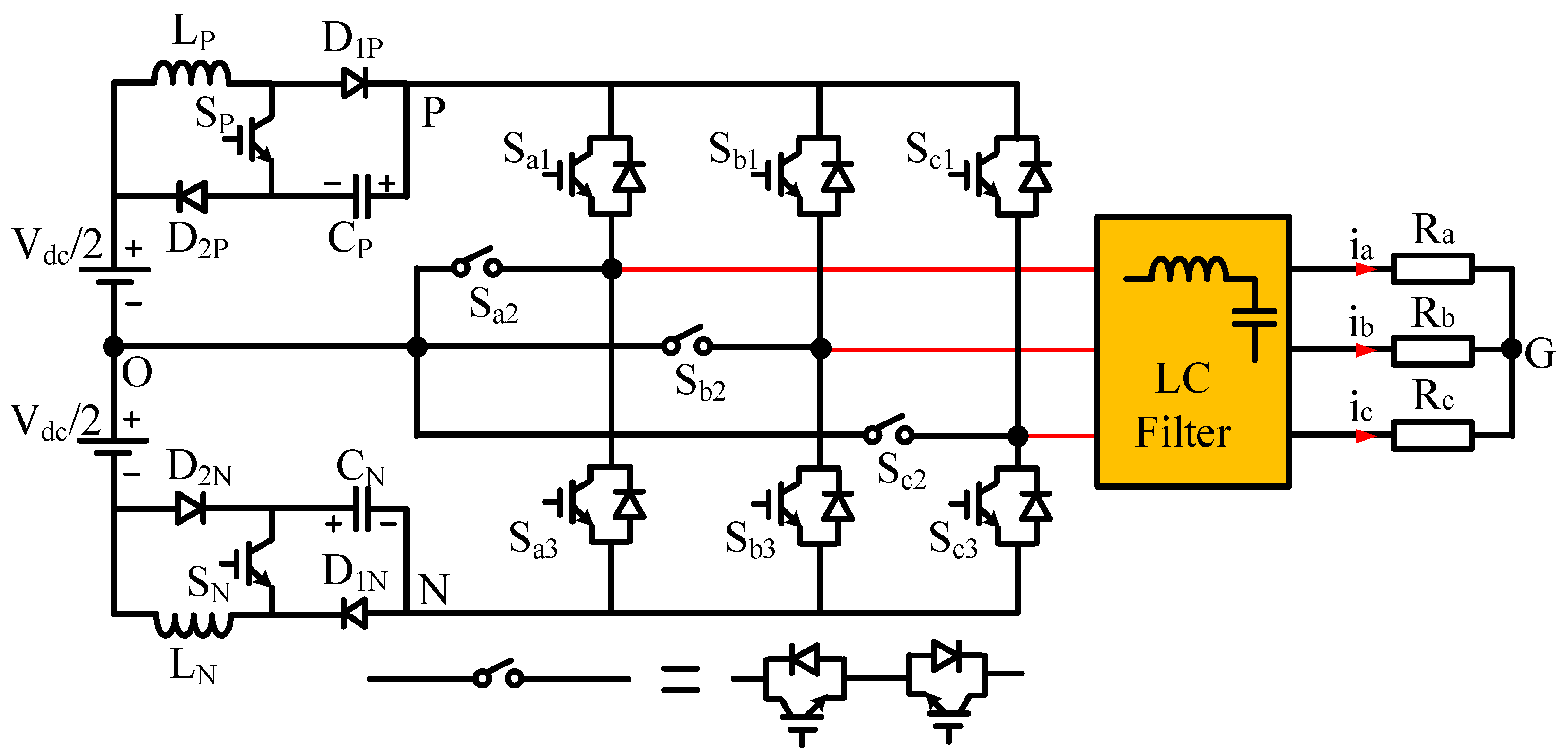
2. Three-Level DC-Link Type Quasi-Switched Boost T-Type Inverter Topology

The 3L-DqSBT2I topology consists of an intermediate network and an inverter leg. The DqSB network is used to connect the input voltage with the 3L-T2I structure to boost the dc-link voltage, as illustrated in Figure 1. The input power supply is split into two equal sources. Each source feeds to an identical DqSB network, which consists of one inductor, one capacitor, two diodes, and one active switch. The 3L-T2I topology is the same as conventional MIs topology which can generate a three-level voltage at output terminal which are +VPN/2, zero, and −VPN/2 which correspond to “P” state, “O” state, and “N” state, respectively, where VPN is the dc-link voltage of the inverter. The output of the inverter feeds to the three-phase resistor load through a three-phase low pass filter (LC filter) to improve the quality of output load voltage as well as the output load current.

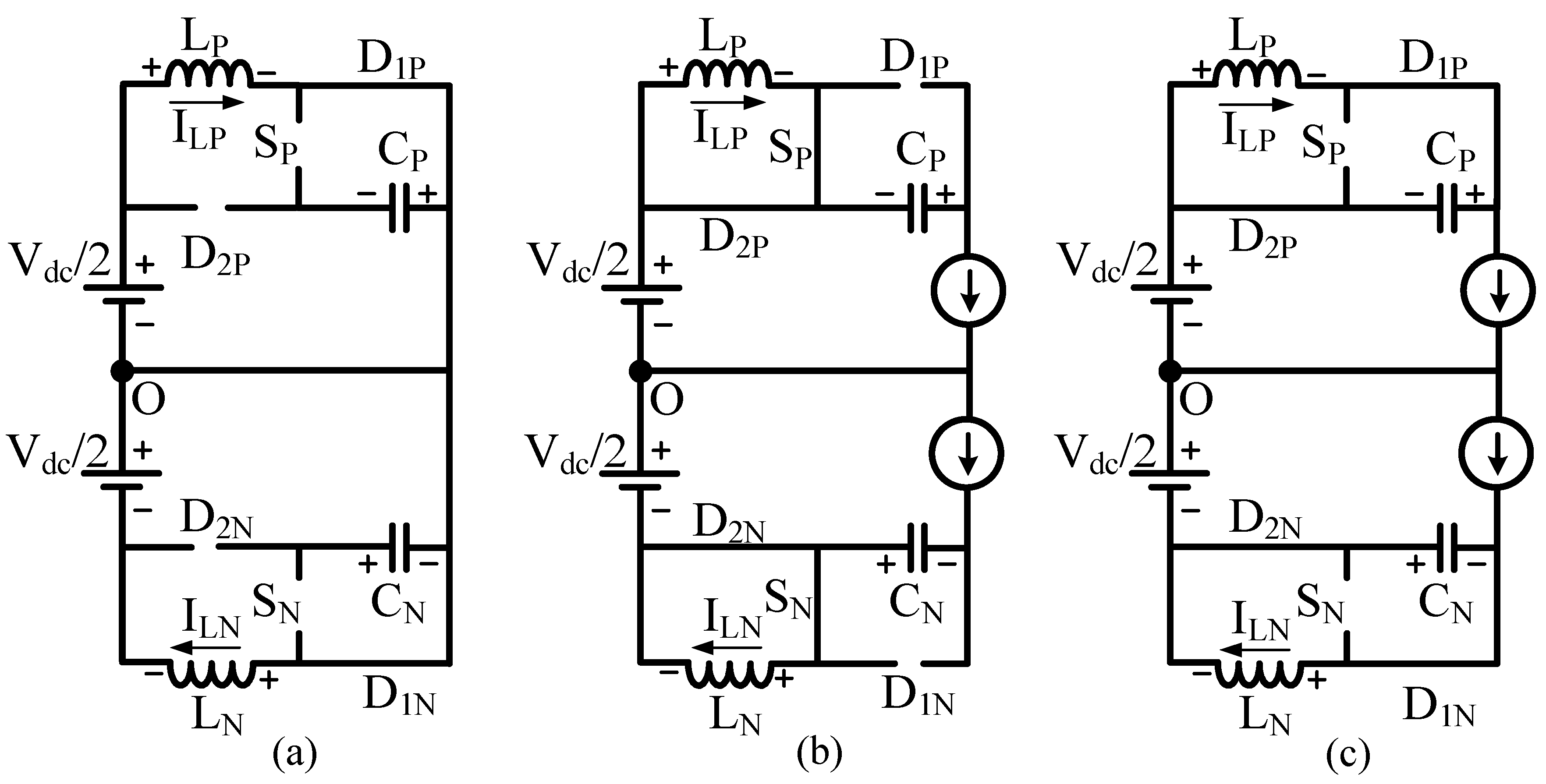
2.1. Operating Principles

Similar to other single-state inverter topologies, this structure also operates under two main modes which are NST and ST modes. In NST mode, the 3L-T2I circuit can produce a three-level voltage at the output terminal by triggering corresponding switches as shown in Table 1. When Sx1 is switched on, the output voltage is achieved +VPN/2 which is the half of dc-link voltage generated by the DqSB network. While the output voltage obtains −VPN/2 when Sx3 is turned on. The zero value is produced at output voltage when Sx2 is triggered on. The NST mode consists of two sub-modes which are NST 1 and NST 2, as presented in Figure 2. The ST mode is achieved when all switches in the inverter leg are triggered on, as a result, the output load voltage in this time interval is zero. Therefore, in order to decrease the waveform distortion at the output, the ST signal is inserted within the time interval when the output voltage is zero.
In NST 1 as shown in Figure 2b, the switches SP and SN are triggered on. Therefore, the diode D1P and D1N are reversed bias whereas diode D2P and D2N are forward bias. The inductors LP and LN are short circuit by active switches and diodes D2P and D2N of the DqSB network. As a result, the current through two inductors is kept constant. The voltages across two inductors are expressed as:
V L P = V L N = 0
In NST 2 as shown in Figure 2c, the switches SP and SN are triggered off, all diodes of the intermediate network are forward bias. As a result, the capacitors CP and CN are charged from LP and LN, respectively. The voltages of these inductors are calculated as:
{ V L P = V C P V L N = V C N
In ST mode, all switches of 3L-T2I are turned on, simultaneously. As a result, the diodes D1P and D1N are forward bias whereas diodes D2P and D2N are reversed bias. The inductors LP and LN store energy from the input power source. The voltages of two inductors are expressed as:
V L P = V L N = V d c / 2

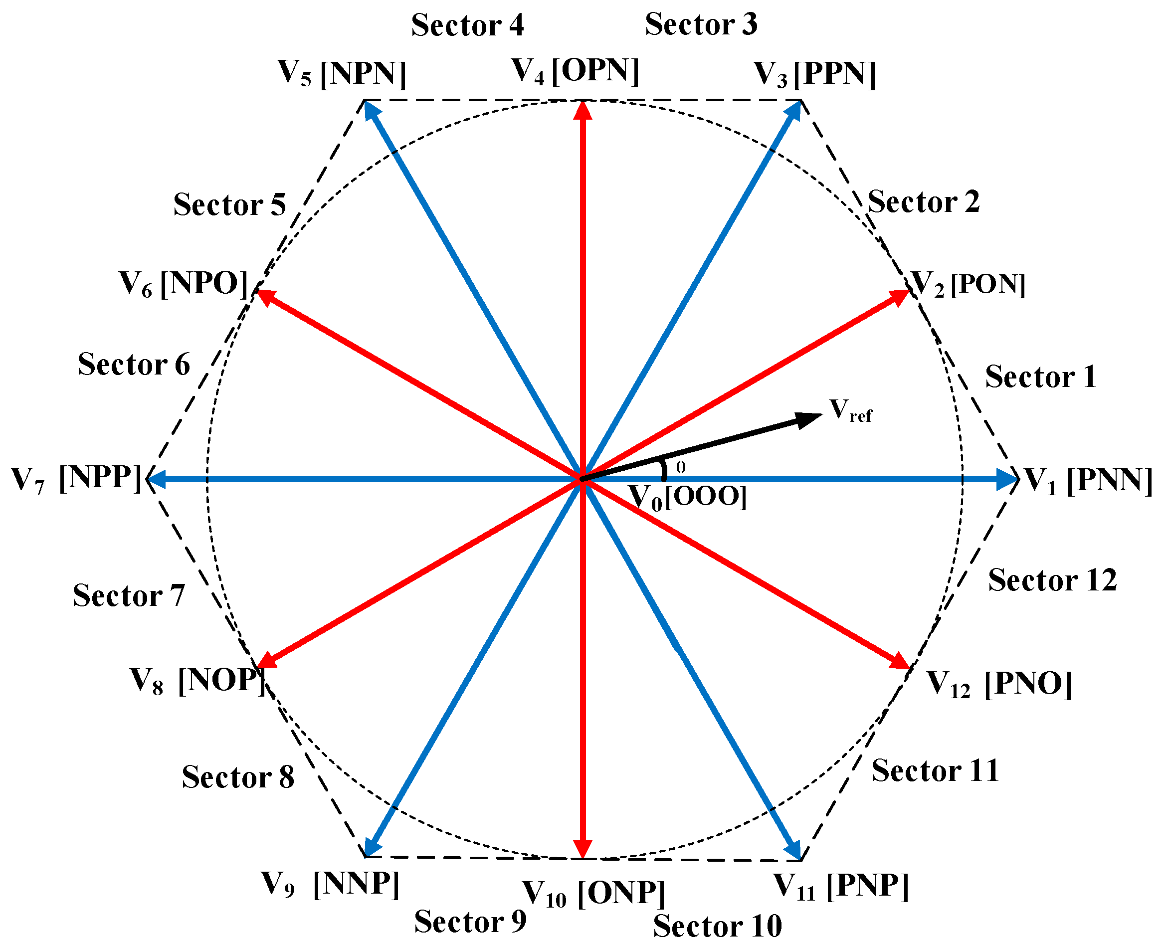
2.2. SVP Scheme to Reduce CMV

In [2,30,32] the authors figured out that the CMV causes some problems in power systems such as electromagnetic interference or bearing current and shaft voltage, etc. Thus, CMV reduction is necessary to enhance the reliability of the system. The CMV generated by the inverter is identified as:
V C M V = V G O = V A O + V B O + V C O 3
where VAO, VBO, and VCO are three-phase output pole voltage.
Based on Equation (4), the magnitude of CMV can be limited from −VPN/6 to +VPN/6 by using only zero vector, medium vectors, and large vectors to synthesize the reference vector during operation of the inverter [2,32]. Thus, the space vector diagram of the three-level inverter is divided into 12 sectors to analyze the operation of the converter, as shown in Figure 3.
In general, assuming that the reference vector ( V r e f ) is located in sector 1 or sector 2, the V r e f is synthesized as follows:
Case 1: When the V r e f is located in sector 1, the V 0 ,   V 1 , and V 2 are adopted to generate the V r e f . Thus, the relationship between these vectors can be expressed as:
{ V r e f T = V 0 T Z + V 1 T L + V 2 T M T = T Z + T M + T L
where,
(1)
V r e f —reference vector,
(2)
V 0 ,   V 1 ,   V 2 —zero vector, large vector, and medium vector, respectively,
(3)
T—switching period of the inverter,
(4)
TZ, TM, TL—the on-times of V 0 ,   V 2 , and V 1 , respectively.
Similar to [2], the drew-time of each vector can be expressed as:
{ T M = 2 m T sin ( θ ) T L = 3 m T sin ( π / 6 θ ) T Z = T T M T L
Case 2: Similar to sector 1, for sector 2, the V r e f can be expressed as:
{ V r e f T = V 0 T Z + V 3 T L + V 2 T M T = T Z + T M + T L
The drew-time of V 0 ,   V 2 , and V 3 can be identified as [2]:
{ T M = 2 m T sin ( π / 3 θ ) T L = 3 m T sin ( θ π / 6 ) T Z = T T M T L
Not similar to the study of [2] which only used the ST signal to boost the dc-link voltage, this topology also uses the active switches of the DqSB network to enhance the dc source. Thus, the switching sequence for sector 1 and sector 2, the ST insertion, and the control signal of DqSB’s switches are reselected, as shown in Figure 4.
By applying this way to other sectors, the drew-time of each vector as well as the switching sequence can be easily identified.

2.3. Steady-State Analysis

In one period of switching (T), the time interval of ST state is (DST·T), while (D0·T) is the time interval of NST 1. Therefore, the value (1 − DST − D0)T is the time interval of NST 2. Applying the volt-second balance for two inductors LP and LN with the note that (VCP = VCN = VC), the voltages across these capacitors can be calculated as:
V C = V C P = V C N = 1 2 D S T 1 D 0 D S T V d c
The inductor current ripple is calculated as:
{ Δ I L P = V d c D S T 4 L P f Δ I L N = V d c D S T 4 L N f
where,
(1)
I L P ,   I L N —inductor current ripples of LP and LN, respectively,
(2)
f —switching frequency of the inverter,
(3)
DST—ST duty ratio,
(4)
D0—duty cycle of SP and SN.
The peak value of dc-link voltage (VPN) is the sum of two capacitors voltage and the dc input source, which is identified as:
V P N = V d c + 2 V C = 1 D 0 1 D 0 D S T V d c
Based on Equation (11) the boost factor (B) can be calculated as:
B = V P N V d c = 1 D 0 1 D 0 D S T
The peak value of first harmonic of output phase voltage (Vx,peak) can be identified as:
V x , p e a k = m 2 3 V P N 2 = m 3 1 D 0 1 D 0 D S T V d c
The voltage gain (G) of the converter is expressed as:
G = V x , p e a k V d c = m 3 1 D 0 1 D 0 D S T
The relationship between modulation index, the ST duty ratio, and the duty cycle of DqSB’s switches are illustrated as:
{ 0 m 1 m + D S T 1 D S T + D 0 < 1

3. Comparison to Other Configurations

To validate the accuracy of the proposed topology and its PWM control method, some investigations about boost factor, voltage gain, and voltage stress on power devices are conducted for the ZS inverter (ZSI) proposed in [8], the qZS inverter (qZSI) introduced in [2,19], the qSB inverter (qSBI) with two sources and two inductors proposed in [35], the qSBI with reducing number of sources and inductors in [36], and the proposed 3L-DqSBT2I.
Table 2 presents the overall comparison between 3L-DqSBT2I and other topologies. It can be seen that the qZSI uses the largest number of passive components (four inductors and four capacitors), while the ZSI, the qSBI in [35], and the 3L-DqSBT2I save two inductors and two capacitors compared to the qZSI. The qSB in [36] uses the smallest number of passive components for the intermediate network which just has one inductor and two capacitors. While, the diode and active switch of the qSBI and the 3L-DqSBT2I are used more than the ZSI and qZSI. Two active switches and four diodes are used for both the qSBI and the 3L-DqSBT2I, while the ZSI and qZSI just use two diodes, as shown in Table 2.
Figure 5 shows the investigations about boost factor versus ST duty ratio and the voltage gain versus modulation index for these topologies and PWM methods, and it is noted that the modulation index is set to (1 − DST) to achieve the highest voltage gain for each scheme. As illustrated in Figure 5a, the boost factor of the 3L-DqSBT2I depends on two coefficients which are the duty cycle of the DqSB network’s active switches (D0) and the ST duty ratio (DST). With the increase of D0, the boost factor of the 3L-DqSBT2I is increased, whereas the boost factor of other topologies is just up to the DST. When the value 0.5 is applied to D0, the 3L-DqSBT2I produces the same boost factor to the other configurations. However, by applying the SVP method, the voltage gain of the ZSI in [8], and the qZSI in [2], the 3L-DqSBT2I has the larger voltage gain which is 2/ 3 times larger than the others, as illustrated in Figure 5b. Similar to the boost factor versus the ST duty ratio, the 3L-DqSBT2I just provides superior in voltage gain when D0 > 0.5. For that reason, in this paper, the value 0.6 was selected for coefficient D0 as an example to analyze the effectiveness of the proposed topology.
Figure 6 shows the investigations of voltage stress on power components such as capacitor voltage stress, diode voltage stress, and switch voltage stress with the note that there are four capacitors in the qZSI with unequal voltage stress on their, as shown in Table 2. Thus, this comparison was conducted for each capacitor of the qZSI. Furthermore, the diode voltage stress of each diode of the qSBI and 3L-DqSBT2I is also not equal to each other. Therefore, the investigation was also carried out for each diode. As presented in Figure 6a, the qZSI is superior in capacitor voltage stress for both methods in [2,19], while the qSBI produces higher voltage stress on the capacitor than the ZSI. In general, the proposed 3L-DqSBT2I is better than the ZSI and qSBI. Moreover, in the range of low voltage gain, the 3L-DqSBT2I is also better than the qZSI. Furthermore, all diodes of 3L-DqSBT2I have less voltage stress compared to other configurations, as shown in Figure 6b. This figure also points out that the qZSI is better than ZSI about voltage stress on diodes with the same voltage gain value. As the impedance-source networks in [2,8,19] do not have any active switches, the ZSI and qZSI are not considered to investigate for switch voltage stress which is shown in Figure 6c. As the voltage stress of the active switch is equal to the capacitor voltage, the 3L-DqSBT2I has less voltage stress on the switch than the qSBI.

4. Simulation and Experimental Results

4.1. Simulation Results

The accuracy of the proposed inverter was validated by simulation results with the help of PSIM software. The parameters used for simulation are listed in Table 3. Before feeding to three-phase resistor load, the three-phase low pass filter was used to mitigate the magnitude of high-frequency harmonics. To produce a root mean square (RMS) output phase voltage of 110 V from the input voltage of 200 V, the modulation index was 0.85. Thus, from Equation (15) the ST duty cycle must be 0.15.
Figure 7 from top to bottom shows the simulation results for input voltage, capacitor voltages, output pole voltage, output phase voltage, and harmonic spectrum. By using 0.6 for D0 and 0.15 for ST duty ratio (DST), as shown in Table 3, the capacitor voltages (VCP and VCN) are boosted to 60 V from 200 V of the dc input source, as illustrated in Figure 7. Therefore, the peak value of dc-link voltage can be identified as 320 V by summing the capacitor voltages and the input voltage. The peak-peak value of output pole voltage is equal to the dc-link voltage which has three levels: 160 V (+VPN/2), zero, and −160 V (−VPN/2), as shown in Figure 7. The output phase voltage has seven levels and its peak-peak value is varied from −2/3VPN to +2/3VPN, as shown in Figure 7. By using the modulation index of 0.85, the peak value of the first order harmonic of output phase voltage is 156 V, approximately, as presented in Figure 7. The THD value of output phase voltage is 54.59%, which is measured by using the harmonic spectrum in Figure 7.
Figure 8 from top to bottom presents the simulation results for dc-link voltage, line-line voltage, and CMV. By using the full ST insertion, the dc-link voltage is varied from zero to the peak-value of dc-link voltage which is 320 V achieved in NST mode. The peak value of output line-line voltage is equal to dc-link voltage, so the top part of VAB is varied from zero to 320 V, as illustrated in Figure 8. The old sectors of space vector diagram produce CMV varying from 0 to −VPN/6, whereas the even sectors produce the CMV which varies from 0 to +VPN/6. Therefore, when applying the introduced method, the CMV frequency is three times larger than the output voltage, and the peak-peak value of it is equal to VPN/3 which varies from −VPN/6 to +VPN/6. The RMS value of CMV is 32.7 VRMS.
Figure 9 from top to bottom shows the simulation results of the inductor current, three-phase output load voltage, and three-phase output load current. The inductor currents of two inductors are equal to each other. The average value of inductor currents is 11.7 and 11.6 A for ILP and ILN, respectively. Due to applying the low-pass filter before the resistor load, the output load voltage, as well as the output load current, have a good quality. The THD value of these waveforms is 2.38% for both voltage and current waveforms. The RMS value of output load voltage and output load current are 111 VRMS and 2.78 ARMS.
Figure 10 shows the simulation results of dc-link voltage, inductor current, DqSB network’s active switch voltage stress, diode voltage stress. The inductor LP stores energy in ST mode which appeared when the diode D2P is reserved bias, as illustrated in Figure 10. In this time interval, the current through LP linearly increases. The inductor current ripples are measured as 1.5 and 1.44 A for LP and LN, respectively. The inductor current is kept constant when SP is turned on and the diode D1P is reserved bias, as shown in Figure 10. As all switches of the inverter branch are triggered on, the DC-link voltage is zero in ST mode, whereas it achieves maximum value in NST mode, as presented in Figure 10.
Figure 11 shows the investigation about voltage gain versus THD value of VAG and voltage gain versus CMV. When the voltage gain increases, the modulation index decreases, which is demonstrated in Section 3. Thus, the THD value of output phase voltage increases with the increase of voltage gain. With all value of voltage gain, the 3L-DqSBT2I method always produces a smaller value of THD value of VAG than that of the SinPWM method in [35], as presented in Figure 11a. Moreover, the RMS value of CMV produced by the 3L-DqSBT2I method is superior to that of the SinPWM method in [35], as illustrated in Figure 11b.

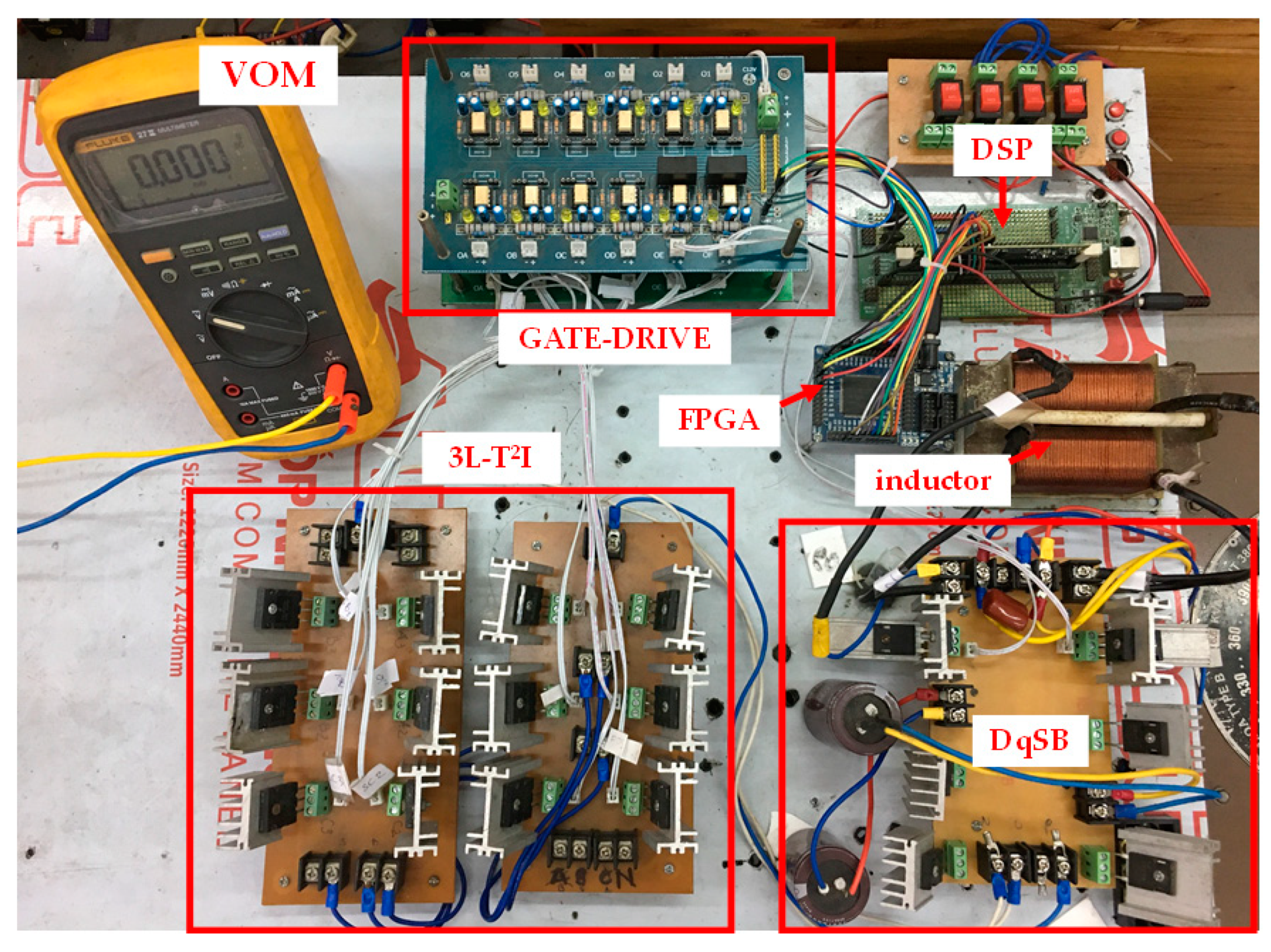
4.2. Experimental Results

The performance of the proposed inverter was further validated through the experiment. A 1 kW prototype was carried out in a laboratory with the parameters listed in Table 3, which is the same as the simulation. This prototype was controlled by a DSP F28335 microcontroller and FPGA Cyclone II EP2C5T144C8. The gate-drive was based on TLP250, which fed to IGBT FGL40N150D, which are low-side and high-side switches of 3L-T2I branch, while IGBT FGL40N120D and MOSFET 6R045A were installed for bidirectional switches and DqSB network’s switches, respectively. The three-phase resistive load was considered to verify the proposed methods, which was fed through three-phase LC filter with the cut-off frequency of approximately 1 kHz by applying 3 mH and 10 μF for inductor value and capacitor value, respectively. The photo of experiment prototype is illustrated in Figure 12. The experimental results are shown in Figure 13.
Figure 13 shows the experimental results of output phase voltage (VAG), CMV, output line-line voltage (VAB), output load voltage (VA), output load current (IA), inductor current (ILP), diode voltage (VD1P and VD2P), dc-link voltage (VPN), dc input voltage (Vdc), capacitor voltage (VCP and VCN), and the harmonic spectrum of output phase voltage and output load current.
The capacitor voltages (VCP and VCN) are, respectively, boosted to 53 and 51 V from 200 V dc input source by applying the ST duty ratio of 0.15 and coefficient D0 of 0.6, as shown in Figure 13c. Therefore, the peak-value of dc-link voltage is 304 V which is the sum of capacitor voltage and dc input power supply, as presented in Figure 13c. The variation of top part of output line-line voltage is from zero to dc-link voltage. The output phase voltage has seven-level voltage which varies from −2/3VPN to +2/3VPN. The form of output load voltage and output load current are sinewave which are achieved by applying LC filter before feeding to the load, as illustrated in Figure 13b. Their RMS values are 104 VRMS and 2.5 ARMS, respectively. The simulated values are nearly the calculated values, whereas the calculated values are higher than the measured values. This is because the SVP method is used to obtain a high voltage gain, and the voltage drops across the devices, caused by high currents, are dominant. The CMV generated by proposed topology when applying introduced method varies from −VPN/6 to +VPN/6, as shown in Figure 13a. The RMS value of CMV is 32.6 VRMS. Figure 13c shows that the inductor current is linearly increased when the dc-link voltage achieves zero value while the diode D2P is reserved bias which represents ST state. While, the constant value of inductor current is obtained when NST mode 1 is achieved, which is represented by reserving bias the diode D1P. Figure 13e,f shows the harmonic spectrum of VAG and IA. It can be seen that the peak-value of the harmonic spectrum of output phase voltage is 104 VRMS at the first-order harmonic of 50 Hz. By using a low-pass LC filter, the magnitude of high-frequency harmonics of VAG is reduced and approximately equal to zero. The magnitude of the first harmonic of the load current, IA is around 2.5 ARMS as illustrated in Figure 13f. Based on the harmonic spectrum analysis, the THD values of output voltage and current can be calculated as 62.4% and 2.77%, respectively.

5. Conclusions

This paper proposed the 3L DqSBT2I configuration which combines all advantages of the 3LT2I and the DqSB network. This configuration is controlled by the SVP technique with some benefits such as enhancing modulation index and reducing the magnitude as well as the slew-rate of CMV. In this scheme, the zero vector, medium vectors, and large vectors were utilized to generate the output voltage. The control signal of intermediate network power switches was also detailed to provide the high boost factor and voltage gain. As a result, the voltage stress on power devices like capacitors, diodes, and switches were decreased significantly. To validate the performance of the proposed method, the PSIM simulation and the laboratory prototype experiment were conducted. Furthermore, the comparisons between the proposed method and other conventional schemes were carried out to confirm the effectiveness of the proposed technique. Due to all benefits mentioned above, this configuration is suitable for low and medium voltage applications like photovoltaic systems or motor drives.

Author Contributions

This paper was a collaborative effort among all authors. V.-T.T., D.-T.D., V.-D.D. and M.-K.N. conceived the methodology, conducted the performance tests and wrote the paper. All authors have read and agreed to the published version of the manuscript.

Funding

This research was funded by T2020-18TĐ project.

Acknowledgments

This work was supported by the Advanced Power Electronics Laboratory, D405 at Ho Chi Minh City University of Technology and Education, Viet Nam.

Conflicts of Interest

The authors declare no conflict of interest.

Nomenclature

3L-T2Ithree-level T-Type inverter
3L-DqSBT2Ithree-Level DC-link type quasi switch boost T-type inverter
Bboost factor of the inverter
CMVcommon-mode voltage
D0duty cycle of DqSB network’s active switches
DqSBdc-link type of the qSB
DSTshoot-through duty ratio
FCflying capacitor
fswitching frequency of the inverter
Gvoltage gain of the inverter
IAA-phase output load current
ILPinductor LP current
I L P inductor current ripple of LP
ILNinductor LN current
I L N inductor current ripple of LN
mmodulation index
MIsmultilevel inverters
NPCneutral point clamped
NSTnon-shoot-through
PVphotovoltaic systems
PWMpulse width modulation
qSBquasi-switch boost
qSBIquasi-switch boost inverter
qZSquasi-Z-source
qZSIquasi-Z-source inverter
RMSroot mean square
STshoot-through
SVPspace vector pulse width modulation
Tswitching period of the inverter
THDtotal harmonic distortion
TMdrew-time of medium vector
TLdrew-time of large vector
TZdrew-time of zero vector
UPSuninterruptable power supply
V 0 zero vector
V 1 ,   V 3 large vectors
V 2 medium vector
VABoutput line-line voltage
VAGA-phase output phase voltage
VAOA-phase output pole voltage
VBOB-phase output pole voltage
VCcapacitor voltage
VCMVcommon-mode voltage
VCNvoltage across CN
VCOC-phase output pole voltage
VCPvoltage across CP
Vdcdc input voltage
VD1Pdiode D1P voltage
VD2Pdiode D2P voltage
VGOcommon-mode voltage
VLPvoltage across LP
VLNvoltage across LN
VPNdc-link voltage
V r e f reference vector
VSPswitch SP voltage
Vx, peakpeak value of the first harmonic of output phase voltage
ZSZ-source
ZSIZ-source inverter

References

  1. Schweizer, M.; Kolar, J.W. Design and Implementation of a Highly Efficient Three-Level T-Type Converter for Low-Voltage Applications. IEEE Trans. Power Electron. 2013, 28, 899–907. [Google Scholar] [CrossRef]
  2. Qin, C.; Zhang, C.; Chen, A.; Xing, X.; Zhang, G. A Space Vector Modulation Scheme of the Quasi-Z-Source Three-Level T-Type Inverter for Common-Mode Voltage Reduction. IEEE Trans. Ind. Electron. 2018, 65, 8340–8350. [Google Scholar] [CrossRef]
  3. Kim, H.S.; Kwon, Y.C.; Chee, S.J.; Sul, S.K. Analysis and Compensation of Inverter Nonlinearity for Three-Level T-Type Inverters. IEEE Trans. Power Electron. 2017, 32, 4970–4980. [Google Scholar] [CrossRef]
  4. Ho, A.V.; Chun, T.W. Topology and Modulation Scheme for Three-Phase Three-Level Modified Z-Source Neutral-Point-Clamped Inverter. IEEE Trans. Power Electron. 2019, 34, 11014–11025. [Google Scholar] [CrossRef]
  5. Guo, X.; Yang, Y.; Wang, B.; Blaabjerg, F. Leakage Current Reduction of Three-Phase Z-Source Three-Level Four-Leg Inverter for Transformerless PV System. IEEE Trans. Power Electron. 2018, 34, 6299–6308. [Google Scholar] [CrossRef]
  6. Zhou, Z.J.; Zhang, X.; Xu, P.; Shen, W.X. Single-Phase Uninterruptible Power Supply Based on Z-Source Inverter. IEEE Trans. Ind. Electron. 2008, 55, 2997–3004. [Google Scholar] [CrossRef]
  7. Sonar, S.; Singh, S. Improved Space Vector PWM Techniques of the Three level ZSI. In Proceedings of the 2019 International Conference on Computing, Power and Communication Technologies (GUCON), NCR New Delhi, India, 27–28 September 2019. [Google Scholar]
  8. Xing, X.; Zhang, C.; Chen, A.; He, J.; Wang, W.; Du, C. Space-Vector-Modulated Method for Boosting and Neutral Voltage Balancing in Z-Source Three-Level T-Type Inverter. IEEE Trans. Ind. Appl. 2016, 52, 1621–1631. [Google Scholar] [CrossRef]
  9. Zhang, J.; Wai, R.J. Novel Space-Vector Pulse-Width-Modulation Mechanism for Three-Level Neutral-Point-Clamped Z-Source Inverter. In Proceedings of the 2019 4th International Conference on Intelligent Green Building and Smart Grid (IGBSG), Yichang, China, 6–9 September 2019. [Google Scholar]
  10. Liu, H.; Chen, A.; Chen, J.; Du, C.; Zhang, C. Hybrid Modulation Strategy for Eliminating Low-Frequency Neutral-Point Voltage Oscillations in Z-Source NPC Three-Level Inverter. In Proceedings of the 2018 IEEE International Power Electronics and Application Conference and Exposition (PEAC), Shenzhen, China, 4–7 November 2018. [Google Scholar]
  11. Zhang, J.; Wai, R.J. Design of New SVPWM Mechanism for Three-Level NPC ZSI via Line-Voltage Coordinate System. IEEE Trans. Power Electron. 2020, 35, 8539–8606. [Google Scholar] [CrossRef]
  12. Ho, A.V.; Huynh, A.T.; Chun, T.W. Three-phase Modified Z-source Three-level T-Type Inverters with Continuous Source Current. In Proceedings of the 2019 International Aegean Conference on Electrical Machines and Power Electronics (ACEMP) & 2019 International Conference on Optimization of Electrical and Electronic Equipment (OPTIM), Istanbul, Turkey, 27–29 August 2019. [Google Scholar]
  13. Anderson, J.; Peng, F.Z. Four quasi-z-Source inverters. In Proceedings of the 2008 IEEE Power Electronics Specialists Conference, Rhodes, Greece, 15–19 June 2008. [Google Scholar]
  14. Stepenko, S.; Husev, O.; Vinnikov, D.; Pimentel, S.P.; Prystupa, A. Experimental Efficiency and Thermal Parameters Evaluation in Full-SiC Quasi-Z-Source Inverter. In Proceedings of the IEEE 60th International Scientific Conference on Power and Electrical Engineering of Riga Technical University (RTUCON) 2019, Riga, Latvia, 7–9 October 2019. [Google Scholar]
  15. Makovenko, E.; Husev, O.; Cadaval, E.R.; Vinnikov, D.; Stepenko, S. Single-Phase Three-Level qZ-Source Inverter Connected to the Grid with Battery Storage and Active Power Decoupling Function. In Proceedings of the International Scientific Conference on Power and Electrical Engineering 2018, Barcelona, Spain, 26–27 July 2018. [Google Scholar]
  16. Stepenko, S.; Husev, O.; Vinnikov, D.; Fesenko, A.; Clemente, C.R.; Pimentel, S.P.; Santasheva, E. Experimental Comparison of Two-Level Full-SiC and Three-Level Si–SiC Quasi-Z-Source Inverters for PV Applications. Energies 2019, 12, 2509. [Google Scholar] [CrossRef] [Green Version]
  17. Stepenko, S.; Husev, O.; Vinnikov, D.; Fesenko, A.; Matiushkin, O. Feasibility Study of Interleaving Approach for Quasi-Z-Source Inverter. Electronics 2020, 9, 277. [Google Scholar] [CrossRef] [Green Version]
  18. Roncero-Clemente, C.; Romero-Cadaval, E.; Pires, V.F.; Martins, J.F.; Vilhena, N.; Husev, O. Efficiency and loss distribution analysis of the 3L-Active NPC qZS inverter. In Proceedings of the 2018 IEEE 12th International Conference on Compatibility, Power Electronics and Power Engineering (CPE-POWERENG 2018), Doha, Qatar, 10–12 April 2018. [Google Scholar]
  19. Pires, V.F.; Cordeiro, A.; Foito, D.; Martins, J.F. Quasi-Z-Source Inverter With a T-Type Converter in Normal and Failure Mode. IEEE Trans. Power Electron. 2016, 31, 7462–7470. [Google Scholar] [CrossRef]
  20. Ruiz-Cortés, M.; Romero-Cadaval, E.; Roncero-Clemente, C.; González-Romera, E.; Husev, O. Evaluation of losses in three-level neutral-point-clamped and T-type quasi-Z-source inverters with modified carrier based modulation method. In Proceedings of the 2017 11th IEEE International Conference on Compatibility, Power Electronics and Power Engineering (CPE-POWERENG), Cadiz, Spain, 4–6 April 2017. [Google Scholar]
  21. Pan, X.; Pang, Z.; Li, L.; Zhao, F. Input Current Ripples Cancellation in A New Three-level Neutral-Point-Clamped Bi-directional Coupled Quasi Z-Source Inverter. In Proceedings of the 2019 IEEE International Conference on Industrial Technology (ICIT), Melbourne, Australia, 13–15 February 2019. [Google Scholar]
  22. Ahmadzadeh, T.; Babaei, I. Improved quasi-Z-source based three-phase three-level neutral point clamped inverter. In Proceedings of the 2018 9th Annual Power Electronics, Drives Systems and Technologies Conference (PEDSTC), Tehran, Iran, 13–15 February 2018. [Google Scholar]
  23. Wang, T.; Wang, X.; He, Y.; Chen, X.; Ruan, X.; Zhang, Z. An Improved Quasi-Z-Source Three-Level T-Type Inverter and Its Modulation Scheme. In Proceedings of the 2020 IEEE Applied Power Electronics Conference and Exposition (APEC), New Orleans, LA, USA, 15–19 March 2020. [Google Scholar]
  24. Aly, M.; Mayorga, N.; Llor, A.M. A Simplified SVPWM Method for Neutral Point Voltage Control and Common Mode Voltage Reduction in Three-Level qZS T-type PV Inverters. In Proceedings of the 2020 IEEE International Conference on Industrial Technology (ICIT), Buenos Aires, Argentina, 26–28 February 2020. [Google Scholar]
  25. Komurcugil, H.; Bayhan, S. PI and Sliding Mode Based Control Strategy for Three-Phase Grid-Tied Three-Level T-Type qZSI. In Proceedings of the IECON 2019—45th Annual Conference of the IEEE Industrial Electronics Society, Lisbon, Portugal, 14–17 October 2019. [Google Scholar]
  26. Nguyen, M.K.; Le, T.V.; Park, S.J.; Lim, Y.C. A Class of Quasi-Switched Boost Inverters. IEEE Trans. Ind. Electron. 2015, 62, 1526–1536. [Google Scholar] [CrossRef]
  27. Nguyen, M.K.; Tran, T.T.; Lim, Y.C. A Family of PWM Control Strategies for Single-Phase Quasi-Switched-Boost Inverter. IEEE Trans. Power Electron. 2019, 34, 1458–1469. [Google Scholar] [CrossRef]
  28. Do, D.T.; Nguyen, M.K. Three-Level Quasi-Switched Boost T-Type Inverter: Analysis, PWM Control, and Verification. IEEE Trans. Ind. Electron. 2018, 65, 8320–8329. [Google Scholar] [CrossRef]
  29. Do, D.T.; Nguyen, M.K.; Quach, T.H.; Tran, V.T.; Blaabjerg, F.; Vilathgamuwa, M. A PWM Scheme for a Fault-Tolerant Three-Level Quasi-Switched Boost T-Type Inverter. IEEE J. Emerg. Sel. Top. Power Electron. 2019. [Google Scholar] [CrossRef] [Green Version]
  30. Do, D.T.; Nguyen, M.K.; Ngo, V.T.; Quach, T.H.; Tran, V.T. Common Mode Voltage Elimination for Quasi-Switch Boost T-Type Inverter Based on SVM Technique. Electronics 2020, 9, 76. [Google Scholar] [CrossRef] [Green Version]
  31. Do, D.T.; Nguyen, M.K.; Quach, T.H.; Tran, V.T.; Le, C.B.; Lee, K.W.; Cho, G.B. Space Vector Modulation Strategy for Three-Level Quasi-Switched Boost T-Type Inverter. In Proceedings of the 2018 IEEE 4th Southern Power Electronics Conference (SPEC), Singapore, 10–13 December 2018. [Google Scholar]
  32. Tran, V.T.; Do, D.T.; Nguyen, M.K.; Nguyen, D.T. Space Vector Modulation Scheme for Three-Level T-Type Quasi-Switched Boost Inverter to Reduce Common Mode Voltage. In Proceedings of the 2019 10th International Conference on Power Electronics and ECCE Asia (ICPE 2019—ECCE Asia), Busan, Korea, 27–30 May 2019. [Google Scholar]
  33. Duong, T.D.; Nguyen, M.K.; Lim, Y.C.; Choi, J.H.; Vilathgamuwa, D.M.; Walker, G. A study on DC-link-type quasi-switched-boost inverters with improved voltage gain. In Proceedings of the 2019 21st European Conference on Power Electronics and Applications (EPE ‘19 ECCE Europe), Genova, Italy, 3–5 September 2019. [Google Scholar]
  34. Nguyen, M.K.; Duong, T.D.; Lim, Y.C.; Choi, J.H.; Vilathgamuwa, D.M.; Walker, G.R. DC-Link Quasi-Switched Boost Inverter With Improved PWM Strategy and its Comparative Evaluation. IEEE Access 2020, 8, 53857–53867. [Google Scholar] [CrossRef]
  35. Sahoo, M.; Keerthipati, S. A Three-Level LC-Switching-Based Voltage Boost NPC Inverter. IEEE Trans. Ind. Electron. 2017, 64, 2876–2883. [Google Scholar] [CrossRef]
  36. Sahoo, M.; Keerthipati, S. Fault tolerant three-level boost inverter with reduced source and LC count. IET Power Electron. 2018, 11, 399–405. [Google Scholar] [CrossRef]
Figure 1. Three-level DC-link type quasi switch boost T-type inverter (3L-DqSBT2I) topology.
Energies 13 03727 g001
Figure 2. Modes of 3L-DqSBT2I: (a) shoot-through (ST), (b) non-shoot-through (NST) 1, (c) NST 2.
Energies 13 03727 g002
Figure 3. Space vector diagram to reduce common-mode voltage (CMV) for 3L-DqSBT2I.
Energies 13 03727 g003
Figure 4. Switching sequence and ST insertion for (a) sector 1 and (b) sector 2.
Energies 13 03727 g004
Figure 5. Investigation about (a) boost factor versus ST duty ratio and (b) voltage gain versus modulation index.
Energies 13 03727 g005
Figure 6. Investigation about (a) capacitor voltage stress versus voltage gain, (b) diode voltage stress versus voltage gain, and (c) switch voltage stress versus voltage gain.
Energies 13 03727 g006
Figure 7. Simulation results of input voltage (Vdc), capacitor voltages (VCP, VCN), output pole voltage (VAO), output phase voltage (VAG), and harmonic spectrum of VAG.
Energies 13 03727 g007
Figure 8. Simulation results of dc-link voltage (VPN), line-line voltage (VAB), and CMV.
Energies 13 03727 g008
Figure 9. Simulation results of inductor current (ILP, ILN), three-phase output load voltage (VA, VB, VC), three-phase output load current (IA, IB, IC).
Energies 13 03727 g009
Figure 10. Simulation results of dc-link voltage (VPN), inductor current (ILP), DqSB network’s active switch voltage stress (VSP), diode voltage stress (VD1P, VD2P).
Energies 13 03727 g010
Figure 11. Comparison of (a) THD value of output phase voltage versus voltage gain, (b) RMS value of CMV versus voltage gain.
Energies 13 03727 g011
Figure 12. Experimental prototype.
Energies 13 03727 g012
Figure 13. Experimental results of 3L DqSBT2I under SVP control method. (a) output phase voltage VAG and common-mode voltage, (b) output line-line voltage VAB, output load voltage VA, output load current IA, (c) inductor current ILP, diode voltages VD1P, VD2P, dc-link voltage VPN, (d) input voltage Vdc, capacitor voltages VCP, VCN, inductor current ILP, (e) harmonic spectrum of VAG, and (f) harmonic spectrum of IA.
Energies 13 03727 g013
Table 1. Switching states of 3L-DqSBT2I (x = a, b, c).
ModeON SwitchesON DiodesVx
NST 1SP, SND2P, D2N+VPN/2, 0 or −VPN/2
NST 2Sx1 or Sx2 or Sx3D1P, D1N, D2P, D2N+VPN/2, 0 or −VPN/2
STSx1, Sx2, Sx3D1P, D1N0
Table 2. Comparison between 3L-DqSBT2I with other configurations and PWM methods.
ZSI in [8]qZSI with PWM in [19]qZSI with PWM in [2]qSBI with PWM in [34]qSBI with PWM in [35]Proposed 3L-DqSBT2I
Boost factor, B1/(1 − 2DST)1/(1 − 2DST)1/(1 − 2DST)1/(1 − 2DST)1/(1 − 2DST)(1 − D0)/(1 −D0DST)
Voltage gain, Gm·B/ 3 m·B/2m·B/ 3 m·B/2m·B/2m·B/ 3
Capacitor voltage stress, Vc/Vdc(1 − DST)BDST·B/2,
(1 − DST)B/2
DST·B/2,
(1 − DST)B/2
B/2B/20.5·DST/(1 − D0 − DST)
Diode voltage stress, VD/VdcBB/2B/2B/2B/20.5·DST/(1 − D0DST), B/2
Switch voltage stress, VS/VdcNANANAB/2B/20.5·DST/(1 − D0 − DST)
Inductors244212
Capacitors244222
Diodes222444
SwitchesNANANA222
Input current rippleVery highSmallSmallSmallSmallHigh
Table 3. Simulation and experiment parameters.
Parameter/ComponentsValues
DC input voltageVdc200 V
Output voltageVx,RMS110 VRMS
Output frequencyfo50 Hz
Carrier frequencyfs5 kHz
ST duty cycleDST0.15
Modulation indexm0.85
Boost inductorsLP = LN1 mH/20 A
CapacitorsC1 = C22200 μF/600 V
LC filterLf and Cf3 mH and 10 μF
DiodeD1P,D2P,D1N,D2NDSEI60-12A (1200 V, 60 A)
SwitchesSP and SN6R045A (650 V, 60 A)
Sx1 and Sx3FGL40N150D (1500 V, 40 A)
Sx2FGL40N120D (1200 V, 40 A)
Resistor loadR40 Ω

