Abstract
The crystallization of hydrogenated amorphous silicon (a-Si:H) is essential for improving solar cell efficiency. In this study, we analyzed the crystallization of a-Si:H via excimer laser annealing (ELA) and compared this process with conventional thermal annealing. ELA prevents thermal damage to the substrate while maintaining the melting point temperature. Here, we used xenon monochloride (XeCl), krypton fluoride (KrF), and deep ultra-violet (UV) lasers with wavelengths of 308, 248, and 266 nm, respectively. Laser energy densities and shot counts were varied during ELA for a-Si:H films between 20 and 80 nm thick. All the samples were subjected to forming gas annealing to eliminate the dangling bonds in the film. The ELA samples were compared with samples subjected to thermal annealing performed at 850–950 °C for a-Si:H films of the same thickness. The crystallinity obtained via deep UV laser annealing was similar to that obtained using conventional thermal annealing. The optimal passivation property was achieved when crystallizing a 20 nm thick a-Si:H layer using the XeCl excimer laser at an energy density of 430 mJ/cm2. Thus, deep UV laser annealing exhibits potential for the crystallization of a-Si:H films for TOPCon cell fabrication, as compared to conventional thermal annealing.
1. Introduction
Silicon is a formidable material in the electronic and photovoltaic industry due to its outstanding electrical performance and abundancy in nature [1,2]. Polycrystalline silicon (poly-Si) thin films have been widely used in thin film transistors to achieve high definition display in large scale [3]. Also, poly-Si plays important role as a passivating layer in high efficiency crystalline silicon (c-Si) solar cells. The crystallization of amorphous silicon (a-Si) has been achieved using various methods such as thermal annealing, solid-phase crystallization, metal-induced crystallization, sequential lateral solidification, and excimer laser annealing (ELA) [4,5,6,7]. The excimer laser is a type of ultra-violet (UV) laser that was first introduced in 1970 by Basov et al. [8]. ELA has been commonly used in the manufacturing of semiconductor integrated circuits. The word “excimer” originates from two words, excimer and dimer, representing a reaction that generates energy [9]. A combination of inert gases, such as Ar, Kr, and Xe, and reactive gases such as F2 and Cl2, can be used as the laser gas in ELA. Excimer lasers are advantageous because they are generated under bias and high pressures, which can stop the surface damage caused by high-temperature process. The gas molecules in a closed state are energized, which generates a laser in the UV range. Although Xe and Kr typically do not form compounds when used in excimer lasers, they produce high-energy electrons that yield high-energy pulses in the excitement induced by the beam. These gaseous elements are transient when they are combined with F2 or Cl2 gas and form bonded molecules. ELA has been gaining popularity in research as well as in the industry, owing to the short wavelength of an excimer laser, which provides excellent processing quality and high productivity [10]. The crystallization of a-Si using ELA was first achieved in 1994 by the Watanabe group [11,12]. Thereafter, this process has attracted significant research attention because it can be used for heating a thin film of a-Si up to its melting point without causing thermal damage to the substrate. This enables the production of high-quality polysilicon layers. Excimer lasers have outperformed other laser sources due to their larger light source and higher energy density. The UV absorption in excimer lasers is also significantly active and can crystallize a-Si within a comparably short period of time [13].
In this study, we attempted to crystallize a-Si using ELA and evaluated the passivation properties of poly-Si. Our primary motivation was to improve the use of excimer lasers as crystallization sources and enable their application in TOPCon solar cell fabrication technology. Three different excimer laser sources were used as the crystallization sources in this study: xenon monochloride (XeCl) excimer (λ = 308 nm), krypton fluoride (KrF) excimer (λ = 248 nm), and deep UV lasers (λ = 266 nm). The thickness of the a-Si film and the energy density of the laser were varied to analyze the crystallinity of a-Si and evaluate its passivation properties. Past studies showed that crystallinity occurred in lower laser energy density; at higher laser energy density, complete melting of the film occurred [14,15]. Additionally, previous reports showed that a high H content in hydrogenated amorphous silicon (a-Si:H) can be laser crystallized with a remarkable decrease in H content after dehydrogenation process, but for device-grade material, the grain boundary defects of crystallized poly-Si should be passivated with hydrogen [16]. This experimental study targeted optimization of the laser energy density as well as discovery of the best a-Si thickness to improve the effectiveness of ELA in high-efficiency c-Si cell fabrication. We studied the ELA of hydrogenated samples to check their potential as device-grade material. We successfully observed the growth of poly-Si as a function of laser energy density and its effectiveness compared to the conventional thermal annealing process. However, additional research is required to reduce the manufacturing cost and material non-uniformity of the ELA process. This process is also unable to completely crystallize an a-Si layer with a thickness exceeding 50 nm due to its shorter optical penetration depth [17,18]. This paper provides insights into the problems that need to be addressed to ensure that ELA can be effectively and cost-effectively applied on the industrial scale.
2. Materials and Methods
During the experimental procedure, poly-Si formed through the crystallization of a-Si:H achieved via heat treatment and ELA. The samples were prepared using phosphorous doped n-type <100> (3–5 Ω·cm, 200 20 µm thick) Czochralski growth wafers. Surface defects were removed using an etchant solution containing sodium hydroxide (NaOH) powder and sodium hypochlorite (NaOCl) solution at 70–80 °C for 10 min. The samples were then cleaned using the standard Radio Corporation of America (RCA 1 and RCA 2) cleaning methods to remove metallic and organic contaminants from the surface; thereafter, each sample was dipped in hydrochloric acid (HCl) and hydrofluoric acid (HF) for 2 min. Subsequently, the samples were cleaned by rinsing with deionized (DI) water and dried carefully under an N2 gas atmosphere [19]. The samples were then immediately transferred to the thermal oxide furnace for the deposition of thermally grown silicon dioxide (SiO2) tunneling layers on both sides of the wafer. An ultra-thin, 1.4 nm tunnel layer SiO2 was grown via thermal oxidation by exposing the silicon wafers to a temperature of 630 °C under an oxygen gas flow of 5 L/min for 30 min. Thereafter, the a-Si:H layer was deposited on both sides of the wafer using plasma-enhanced chemical vapor deposition (PECVD) with silane (SiH4) and phosphine (PH3) gas at a ratio of 1:1. The thickness of the a-Si:H layer was varied from 20 to 80 nm by controlling the flow rate of H2 gas during PECVD. The samples were then subjected to furnace annealing (FA) (i.e., heat treatment) and ELA to realize the crystallization of a-Si:H. Heat treatment was performed by varying the temperatures between 850 and 950 °C for 30, 60, and 90 min. When the heat treatment temperature exceeded 900 °C, the tunnel oxide layer was partially damaged due to the high temperature, resulting in a decrease in the passivation effect. Another set of samples was prepared for ELA; these samples were first subjected to dehydrogenation via rapid thermal processing at 450 °C for 60 min to eliminate dangling bonds prior to conducting ELA. The samples were then subjected to ELA using three different lasers: XeCl excimer, KrF excimer, and deep UV lasers at wavelengths of 308, 248, and 266 nm, respectively. The energy density of the XeCl excimer laser was varied from 390 to 450 mJ/cm2 for a-Si:H film thicknesses of 20, 40, 60, and 80 nm. The energy density of the KrF excimer laser was maintained at 140 mJ/cm2, while the shot count was changed from 1 to 10 for the same a-Si:H film thickness variation as mentioned for the earlier process. Finally, deep UV laser annealing was performed at an energy density of 660–1980 mJ/cm2 for a fixed a-Si film thickness of 20 nm and a fixed scan speed of 5 mm/s. The thickness of a-Si:H layer was confirmed from nanoview ellipsometry. Raman spectroscopy for ellipsometry (VASE, JA Woollam, 240 < λ < 1700 nm) was used to measure the crystallinity and passivation by measuring carrier lifetime (τeff) and implied open circuit voltage (i-VOC) using the WCT Sintrom-120 QSSPC measuring system [20,21,22]. The experimental results indicated significant progress in crystallization when using ELA compared to that achieved using conventional thermal treatment methods. The heat treatment methods were unable to uniformly crystallize the entire thin film, whereas ELA enabled the selection of a target area for crystallization and the control of the laser energy density [23]. The deep UV ELA samples were subjected to X-ray diffraction (XRD) studies to confirm the crystallinity and increase in grain size (XRD, machine type: Bruker D8 Advance) [24]. The XRD study also confirmed the crystallization of a-Si:H by ELA. These advantages motivated us to employ this experimental approach and find future scopes of ELA for the crystallization of amorphous silicon. A detailed discussion of the experimental results is presented in the following section.
3. Results and Discussions
3.1. Crystallization of a-Si:H Using Heat Treatment
The crystallization of a-Si:H requires a significantly high temperature, which increases the probability of damage to or failure of the sample. Previous studies reported that the minimum temperature required for crystallization of a-Si:H is 600 °C. In this study, crystallization of a-Si:H was conducted at 850–950 °C for 30, 60, and 90 min. Figure 1a presents the Raman shift of the samples subjected to thermal annealing. The sample heated to 900 °C for 30 min exhibited an intense Raman peak. As the thermal annealing temperature increased, the a-Si peak intensity decreased and the poly-Si peak increased and sharpened up to 950 °C. The degree of poly-crystallization and grain growth occurring was clearly observed. However, as the annealing time increased at 950 °C, the agglomeration of poly-Si was observed. A previous study showed that Raman spectra of a-Si:H and poly-Si are located around 480 cm−1 and 500–515 cm−1, respectively [25,26]. The Raman spectra in this study confirmed the peak appears around 515–520 cm−1, and the peak intensity increased as the annealing temperature and time increased. Figure 1b shows the crystallinity as a function of annealing temperature and time. The crystallinity increased with the increase in temperature up to 900 °C. A longer annealing time resulted in degradation of crystallinity. Figure 1c depicts the change in τeff and i-VOC as a function of the heating temperature for the three different treatment times. This figure shows that the optimal passivation property was observed when the samples were treated at 900 °C for 30 min after the forming gas annealing (FGA) treatment, with τeff of 726 µs and i-VOC of 697 mV. Samples subjected to significantly high temperatures for longer treatment times have a higher probability of undergoing damage to or failure of their passivation layer. A maximum crystallinity of 98.38% was attained when the sample was annealed at 875 °C for 90 min. The degree of crystallinity increased with the heat treatment time and temperature; however, there was a noticeable reduction in the passivation property. This reduction is attributed to the damage in the surface passivation layer caused by exposure to high temperatures for longer treatment times. At such high temperatures, blistering occur and pinholes are created in the passivation layer [27,28].
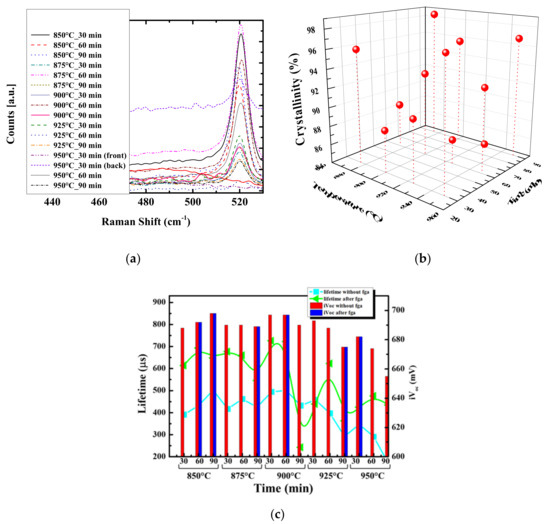
Figure 1.
(a) Raman spectroscopy; (b) change in crystallinity of the a-Si:H thin film after thermal annealing; (c) change in the passivation property as a function of the heating temperatures for three different process times.
3.2. Crystallization of a-Si Using Excimer Laser Annealing
Details regarding the a-Si layer crystallization and the evaluation of the passivation property are described in this subsection. As discussed previously, ELA using the deep UV laser was conducted at a laser energy density of 660–1980 mJ/cm2 with a fixed scan speed of 5 mm/s. The crystallinity and passivation property of the crystallized poly-Si were observed and analyzed. Figure 2a shows the Raman spectra with the increase in laser energy density. As the laser energy density increased, the a-Si peak intensity decreased and the poly-Si peak increased up to 990 mJ/cm2 energy density. The degree of poly-crystallization and grain growth was clearly observable. The Raman spectra showed that the peak appeared around 515 cm−1, confirming crystallization of poly-Si. The peak intensity reached a maximum at 990 mJ/cm2. However, further increase in laser energy density resulted in a drastic fall in the peak of poly-Si in Raman shift, indicating the agglomeration of poly-Si. Figure 2b indicates the degree of crystallinity initially increases with an increase in the laser energy density; however, it began to decrease beyond a certain threshold of the energy density. An energy density exceeding 990 mJ/cm2 resulted in damage to the poly-Si membrane, thereby breaking the lattice structure. The crystallinity also impacted the crystal size, as shown below. Laser energy density also influenced the passivation property of the crystallized a-Si layer. Figure 2c indicates that τeff and i-VOC significantly increased when the laser energy density increased from 660 to 990 mJ/cm2; on increasing the energy density further, τeff and i-VOC decreased considerably. The passivation property was highest when τeff and i-VOC were 384 µs and 654 mV, respectively, with a crystallinity of approximately 98%. Figure 2d shows the XRD analysis of the samples subjected to deep UV ELA with different laser energy densities. The highest peak intensity was observed from this figure at 990 mJ/cm2, with a laser energy density around 2θ = 28.39, corresponding to Si (111). The figure shows the increase in laser energy density resulted in the decrease in peak intensity, corresponding to Si (111), indicating the degradation in crystallinity. The crystalline size was calculated by the Scherrer equation [29]:
where θ is the diffraction angle, D is crystalline size, λ is X-ray wavelength, Δ(2θ) is the full width half maximum (FWHM), and K is constant. The values of λ and K in this experimental study were 1.54 Å and 0.9, respectively. Table 1 shows the crystalline size of poly silicon film with varying laser energy density along with the crystallinity.
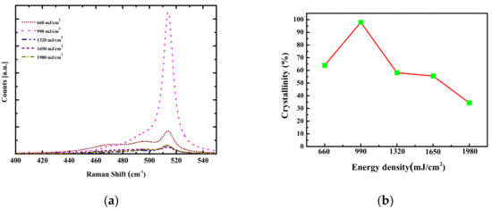
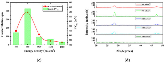
Figure 2.
(a) Raman spectroscopy; (b) change in crystallinity of the a-Si:H thin film after deep UV ELA for various laser energy densities; (c) change in the passivation property as a function of laser energy density for the crystallization of a 20 nm thick a-Si:H layer; (d) XRD of the crystallize a-Si:H thin film subjected to deep UV laser annealing for different energy density.

Table 1.
The crystalline size and crystallinity of the a-Si:H thin film obtained from deep UV laser annealing for different laser energy density.
The surface morphology of the samples subjected to deep UV laser annealing was also observed from field emission scanning electron microscopy (FESEM) images. The images shown in Figure 3a,b indicate that the grain size of globular crystallites increased with an increase in energy density up to 990 mJ/cm2; in Figure 3c, the broken lattice structure shown was caused by the energy density exceeding 990 mJ/cm2. These FESEM images confirmed that higher laser energy density results in a broken lattice structure, resulting in degradation in crystallinity.
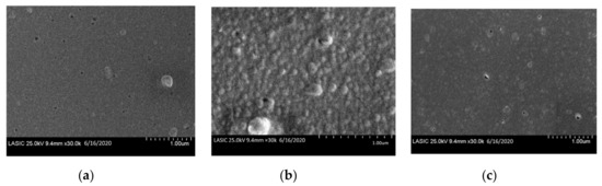
Figure 3.
SEM images of the a-Si:H films after crystallization via deep UV ELA at energy densities of (a) 660, (b) 990, and (c) 1320 mJ/cm2.
During the crystallization of a-Si using the XeCl excimer laser, the energy density was varied from 390 to 450 mJ/cm2, with a varied a-Si layer thickness of 20–80 nm. The samples were cured at 900 °C for 60 min to achieve higher oxidation and better passivation. Figure 4 presents the passivation property observed under these conditions. This figure indicates that the oxidation during ELA increased as the a-Si layer thickness decreased and the laser energy density increased; this occurred because the optical penetration depth for ELA is shorter, making it difficult to crystallize thick a-Si layers. When the laser energy density exceeded 430 mJ/cm2, the passivation property decreased due to damage to the a-Si layer.
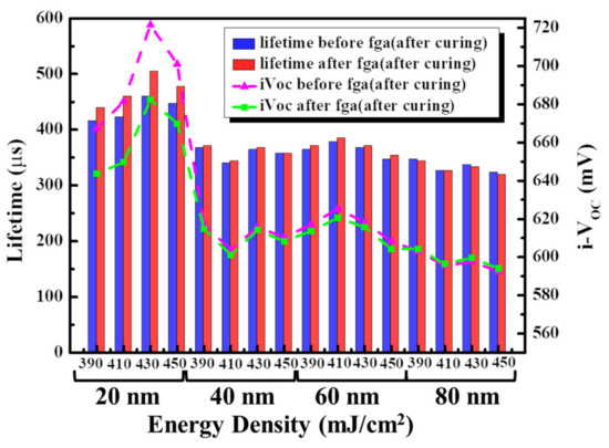
Figure 4.
Variation in the passivation property as a function of the energy density of the XeCl excimer laser for four different a-Si:H layer thicknesses.
The crystallization of a-Si:H using KrF excimer laser was performed. The laser energy density was kept constant at 140 mJ/cm2 while varying the laser shot count from 1 to 10 for a-Si layer thicknesses of 20–80 nm. The samples were subjected to curing at 900 °C prior to ELA, and FGA was conducted subsequently. This significantly improved passivation. Figure 5a,b indicate the variation in the passivation property as a function of the a-Si layer thickness for laser shot counts of 1 to 10. This figure shows that the passivation property increased with the laser shot count in the case of a thin a-Si:H layer; however, an increase in the thickness of the a-Si layer significantly reduced the passivation property. Highest τeff and i-VOC values of 353 µs and 674 mV, respectively, were obtained after the FGA process as shown in Figure 5a. However, the experimental results also indicated that the ELA process conditions need to be further optimized to reduce manufacturing costs and enable the large-scale application of this technique for efficient production.
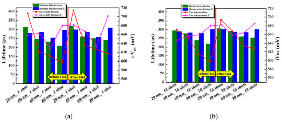
Figure 5.
Variation in the passivation property of the a-Si:H film after crystallization via KrF ELA for (a) 1 and (b) 10 shots count.
4. Conclusions
This experimental study focused on the crystallization of an a-Si:H layer using ELA instead of the conventional thermal annealing to prevent damage to the sample caused by the high-temperature process. The potential of ELA to become a key method for crystallization in the photovoltaic and opto-electronic device market was demonstrated in this paper. The sample subjected to deep UV laser annealing at an energy density of 990 mJ/cm2 exhibited a high degree of crystallinity. This indicates the potential applicability of ELA for crystallization compared to the conventional heat treatment processes. However, the value of τeff achieved via heat-treatment crystallization was 727 µs, which is higher than that achieved using ELA (588 µs). This outcome suggests that the ELA process requires further optimization for achieving high passivation properties in the crystallized a-Si:H layer. Hence, additional research is required to control the laser energy density, laser shot counts, and process time, with the aim of improving passivation properties of the crystallized layer. The XeCl and KrF excimers lasers also yielded improved crystallinity in thin a-Si layers; however, their performances degraded when the thickness of the layer increased. Hence, these excimer lasers are not suitable because a-Si:H layers used as passivation layers in c-Si solar cells are required to have higher thicknesses. This research provides valuable insights into the necessity of optimizing the ELA conditions, with the aim of increasing the optical penetration depth and controlling the energy density. This technology should be cost effective to ensure its wide-spread application for manufacturing high-efficiency solar cells.
Author Contributions
Writing—original draft S.C.; Data Curation—S.C., S.K., J.P., J.K., and Y.K.; Formal Analysis—E.-C.C., G.T.C.; Project—Administration, Y.K., E.-C.C., Y.C., and J.Y.; Supervision—J.Y.; Writing—review & editing—G.T.C. and E.-C.C. All authors have read and agreed to the published version of the manuscript.
Funding
This Research is funded by the Korea Institute of Energy Technology Evaluation and Planning grant funded by the Korea Government.
Acknowledgments
This work was supported by the Korea Institute of Energy Technology Evaluation and Planning (KETEP) and the Ministry of Trade, Industry and Energy (MOTIE) of the Republic of Korea (No. 20194010000090 and 20183010014270).
Conflicts of Interest
The authors declare no conflict of interest.
References
- Dassow, R.; Köhler, J.R.; Grauvogl, M.; Bergmann, R.B.; Werner, J. Laser-Crystallized Polycrystalline Silicon on Glass for Photovoltaic Applications. Solid State Phenom. 1999, 67, 193–198. [Google Scholar] [CrossRef]
- Staebler, D.L.; Wronski, C.R. Reversible conductivity changes in discharge-produced amorphous Si. Appl. Phys. Lett. 1977, 31, 292–294. [Google Scholar] [CrossRef]
- Mei, P.; Boyce, J.B.; Hack, M.; Lujan, R.; Ready, S.E.; Fork, D.K.; Johnson, R.I.; Anderson, G.B. Grain growth in laser dehydrogenated and crystallized polycrystalline silicon for thin film transistors. J. Appl. Phys. 1994, 76, 3194–3199. [Google Scholar] [CrossRef]
- Im, J.S.; Kim, H.J.; Thompson, M.O. Phase transformation mechanisms involved in excimer laser crystallization of amorphous silicon films. Appl. Phys. Lett. 1993, 63, 1969–1971. [Google Scholar] [CrossRef]
- Miyasaka, M.; Stoemenos, J. Excimer laser annealing of amorphous and solid-phase-crystallized silicon films. J. Appl. Phys. 1999, 86, 5556–5565. [Google Scholar] [CrossRef]
- Smith, P.M.; Carey, P.G.; Sigmon, T.W. Excimer laser crystallization and doping of silicon films on plastic substrates. Appl. Phys. Lett. 1997, 70, 342–344. [Google Scholar] [CrossRef]
- Song, D.; Inns, D.; Straub, A.; Terry, M.L.; Campbell, P.; Aberle, A.G. Solid phase crystallized polycrystalline thin-films on glass from evaporated silicon for photovoltaic applications. Thin Solid Film. 2006, 513, 356–363. [Google Scholar] [CrossRef]
- Brotherton, S.D.; McCulloch, D.J.; Clegg, J.B.; Gowers, J.P. Excimer-laser-annealed poly-Si thin-film transistors. IEEE Trans. Electron Devices 1993, 40, 407–413. [Google Scholar] [CrossRef]
- Komotori, J.; Lee, B.J.; Dong, H.; Dearnley, P.A. Corrosion response of surface engineered titanium alloys damaged by prior abrasion. Wear 2001, 251, 1239–1249. [Google Scholar] [CrossRef]
- Sato, H.; Nishio, S. Polymer laser photochemistry, ablation, reconstruction, and polymerization. J. Photochem. Photobiol. C Photochem. Rev. 2001, 2, 139–152. [Google Scholar] [CrossRef]
- Love, R.A.; Parge, H.E.; Wickersham, J.A.; Hostomsky, Z.; Habuka, N.; Moomaw, E.W.; Adachi, T.; Hostomska, Z.J.C. The crystal structure of hepatitis C virus NS3 proteinase reveals a trypsin-like fold and a structural zinc binding site. Cell 1996, 87, 331–342. [Google Scholar] [CrossRef]
- Mohan, S. Fiber Optics and Laser Instrumentation: (for EEE, EI, Electronics, Computer Science & Engineering, Physics and Materials Science Students in Indian Universities); MJP Publisher: Tamil Nadu, India, 2019. [Google Scholar]
- Carluccio, R.; Cina, S.; Fortunato, G.; Friligkos, S.; Stoemenos, J. Structure of poly-Si films obtained by laser annealing. Thin Solid Film. 1997, 296, 57–60. [Google Scholar] [CrossRef]
- Kuriyama, H.; Nohda, T.; Ishida, S.; Kuwahara, T.; Noguchi, S.; Kiyama, S.; Tsuda, S.; Nakano, S. Lateral Grain Growth of Poly-Si Films with a Specific Orientation by an Excimer Laser Annealing Method. Jpn. J. Appl. Phys. 1993, 32, 6190–6195. [Google Scholar] [CrossRef]
- McCulloch, D.J.; Brotherton, S.D. Surface roughness effects in laser crystallized polycrystalline silicon. Appl. Phys. Lett. 1995, 66, 2060–2062. [Google Scholar] [CrossRef]
- Boyce, J.B.; Mei, P. Laser Crystallization for Polycrystalline Silicon Device Applications. In Technology and Applications of Amorphous Silicon; Street, R.A., Ed.; Springer: Berlin/Heidelberg, Germany, 2000; pp. 94–146. [Google Scholar]
- Bidin, N.; Ab Razak, S.N. ArF Excimer Laser Annealing of Polycrystalline Silicon Thin Film. In Crystallization: Science and Technology; Intech Open Publisher: London, UK, 2012; p. 481. [Google Scholar]
- Kühnapfel, S.; Severin, S.; Kersten, N.; Harten, P.; Stegemann, B.; Gall, S. Multi crystalline silicon thin films grown directly on low cost soda-lime glass substrates. Sol. Energy Mater. Sol. Cells 2019, 203, 110168. [Google Scholar] [CrossRef]
- Mallem, K.; Kim, Y.J.; Hussain, S.Q.; Dutta, S.; Le, A.H.T.; Ju, M.; Park, J.; Cho, Y.H.; Kim, Y.; Cho, E.-C.; et al. Molybdenum oxide: A superior hole extraction layer for replacing p-type hydrogenated amorphous silicon with high efficiency heterojunction Si solar cells. Mater. Res. Bull. 2019, 110, 90–96. [Google Scholar] [CrossRef]
- Kimmerle, A.; Rothhardt, P.; Wolf, A.; Sinton, R.A. Increased Reliability for J0-analysis by QSSPC. Energy Procedia 2014, 55, 101–106. [Google Scholar] [CrossRef]
- Koo, K.; Kim, S.; Choi, P.; Kim, J.; Jang, K.; Choi, B. Electrical evaluation of the crystallization characteristics of excimer laser annealed polycrystalline silicon active layer. Jpn. J. Appl. Phys. 2018, 57, 106503. [Google Scholar] [CrossRef]
- Mall, A.K.; Paul, B.; Garg, A.; Gupta, R. Temperature dependent X-ray diffraction and Raman spectroscopy studies of polycrystalline YCrO3 ceramics across the TC ~460 K. J. Raman Spectrosc. 2020, 51, 537–545. [Google Scholar] [CrossRef]
- Pangal, K.; Sturm, J.C.; Wagner, S.; Büyüklimanli, T.H. Hydrogen plasma enhanced crystallization of hydrogenated amorphous silicon films. J. Appl. Phys. 1999, 85, 1900–1906. [Google Scholar] [CrossRef]
- Meador, J.A. A Radiological Survey of Two Bruker D8 Advance XRD Instruments Located in Separate Quality Control Laboratories; West Virginia University Research Repository: Morgantown, WV, USA, 2016. [Google Scholar]
- Saleh, R.; Nickel, N.H. Raman spectroscopy of doped and compensated laser crystallized polycrystalline silicon thin films. Surf. Coat. Technol. 2005, 198, 143–147. [Google Scholar] [CrossRef]
- Yoo, W.S.; Ishigaki, T.; Ueda, T.; Kang, K.; Kwak, N.Y.; Sheen, D.S.; Kim, S.S.; Ko, M.S.; Shin, W.S.; Lee, B.S.; et al. Grain size monitoring of 3D flash memory channel poly-Si using multiwavelength Raman spectroscopy. In Proceedings of 2014 14th Annual Non-Volatile Memory Technology Symposium (NVMTS), Jeju Island, Korea, 27–29 October 2014; pp. 1–4. [Google Scholar]
- Morisset, A.; Cabal, R.; Grange, B.; Marchat, C.; Alvarez, J.; Gueunier-Farret, M.-E.; Dubois, S.; Kleider, J.-P. Highly passivating and blister-free hole selective poly-silicon based contact for large area crystalline silicon solar cells. Sol. Energy Mater. Sol. Cells 2019, 200, 109912. [Google Scholar] [CrossRef]
- Spruiell, J. A Review of the Measurement and Development of Crystallinity and Its Relation to Properties in Neat Poly (Phenylene Sulfide) and Its Fiber Reinforced Composites; Oak Ridge National Lab. (ORNL): Oak Ridge, TN, USA, 2005. [Google Scholar]
- Monshi, A.; Foroughi, M.R.; Monshi, M.R. Modified Scherrer equation to estimate more accurately nano-crystallite size using XRD. World J. Nano Sci. Eng. 2012, 2, 154–160. [Google Scholar] [CrossRef]


© 2020 by the authors. Licensee MDPI, Basel, Switzerland. This article is an open access article distributed under the terms and conditions of the Creative Commons Attribution (CC BY) license (http://creativecommons.org/licenses/by/4.0/).