1. Introduction
The optimization of the characteristics of the front electrodes of solar cells is important in two major aspects—improving conversion efficiency and reducing production costs, which are the main aims while fabricating solar cells. In the solar cell industry, screen printing technologies occupy most of the market share of the metallization of front and rear sides [
1,
2,
3,
4]. Based on the advantages of manufacturing cost and throughput, the technology of the screen-printing process has continuously improved, and the technological improvement in conversion efficiency can be largely divided into two aspects. The first is minimizing the shading loss by applying fine-line printing to absorb as much light as possible [
5], and the second is minimizing the series resistance to reduce electrical loss when the carriers generated by the absorbed light are collected at the electrode [
6]. For fine-line printing, techniques such as changing the emulsion thickness and the application of a knotless screens were applicable to both p- and n-type substrates regardless of the substrate type [
7,
8].
However, when decreasing the series resistance (specifically contact resistance (Rc)), changes in substrate type are significant factors. For p-type substrates, an emitter is formed using phosphorus, and phosphorus atoms penetrate the phosphorus silicate glass (PSG) layer and do not out-diffuse. As a result, the phosphorus atoms accumulate on the surface; thus, the carrier concentration on the surface is the highest [
9,
10]. In contrast, for n-type substrates, boron atoms penetrate the borosilicate glass (BSG) and diffuses out, thereby forming a “deficient layer” with a relatively low boron concentration on the surface [
11]. When a deficient layer is formed, there are limitations to reducing the Rc when using Ag paste. This is because the Rc (resistivity) and emitter surface concentration have the following formula [
12]:
where
ρco is a constant dependent on the metal and semiconductor. The specific contact resistivity (
ρc) primarily depends on the metal-semiconductor work function (
ΦΒ), doping density (
N), and effective mass of the carrier (
m*). Therefore, the paste of the n-type substrate solar cell contains a certain amount of Al to compensate for the deficient layer. It is similar to the formation of the local back surface field (LBSF) of the p-type passivated emitter and rear cell (PERC) structure, where Al reacts with Si and heat to form a p+ region when an alloy is formed. A small amount of Al in the front paste aids in improving the properties of the front contact.
In this study, the contact formation between p+ diffused Si layers and Ag–Al paste with respect to the firing conditions were qualitatively and quantitatively analyzed using scanning electron microscopy (SEM) and energy-dispersive X-ray spectroscopy (EDS). Based on the analysis, we aimed at describing the bonding pattern according to the temperature using a schematic diagram. Finally, the output characteristics of the n-type c-Si solar cell fabricated under optimized conditions were analyzed.
2. Experimental Details
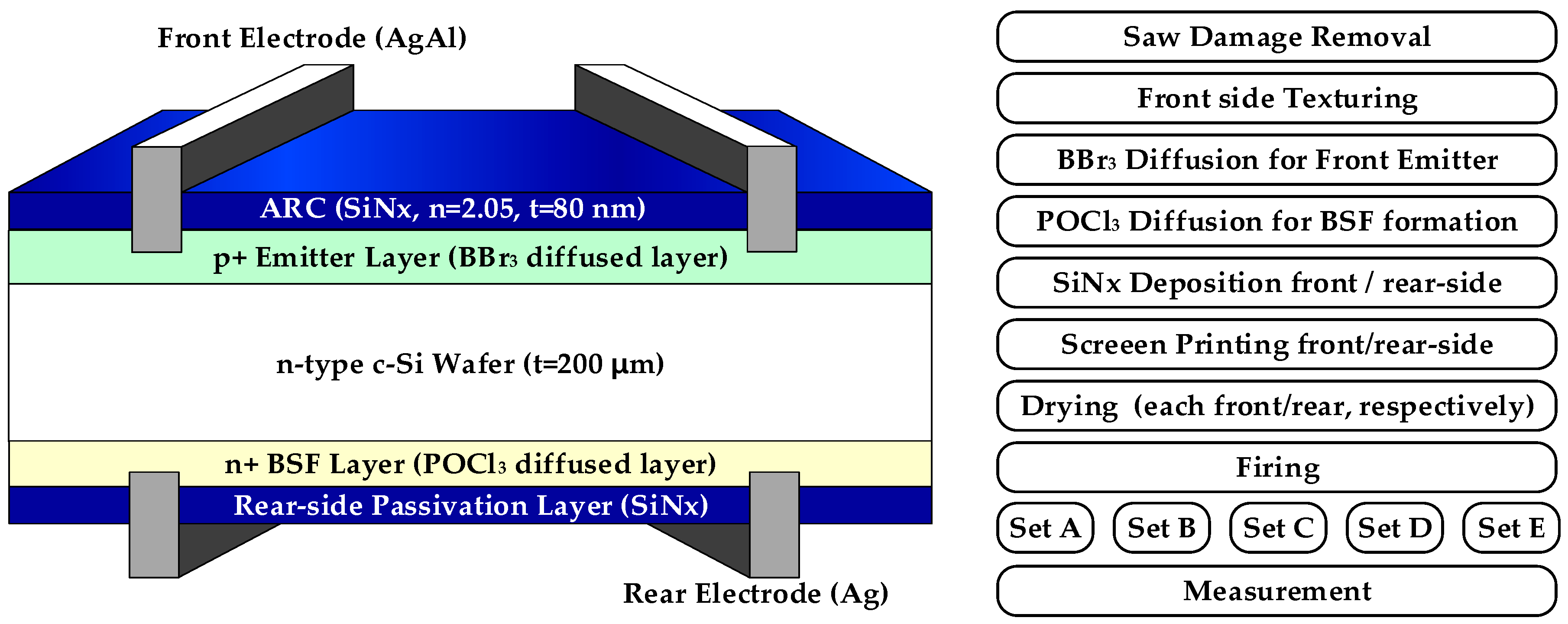
Figure 1 shows the schematic of the solar cell structure and process flow used in this study. Here, 200-μm thick n-type solar-grade Czochralski (Cz-Si) grown wafers with a crystal orientation of (100) and resistivity of 1.5 ohm-cm were used as the starting material for the sample to be analyzed and fabricated into a solar cell. To reduce the reflectance of the Si wafer, the sample was textured using 2% NaOH and 8.75% isopropanol at a temperature range of 84 to 86 °C. The textured wafers were doped with boron using a thermal diffusion process in a furnace using BBr
3 as the dopant source at 910 °C, 5 min pre-deposition, and 1000 °C, 7.5 min drive-in step. After the diffusion process, BSG was removed by dipping the wafer in a diluted hydrofluoric acid (HF) solution, followed by DI-water rinsing and drying. The emitter-sheet resistance was changed to 80 ohm/sq using an etch-back method to remove the boron-rich layer (BRL) using an HF–HNO
3–CH
3COOH mixture. The n+ back surface field was formed by diffusing phosphorus with phosphoryl chloride (POCl
3) diffusion via 810 °C, 7 min pre-deposition and 880 °C, 5 min drive-in step using the dopant source.
Then, 80-nm thick SiNx layers with a refractive index of 2.05 were deposited on the front side for both the passivation and anti-reflection coating layers using a plasma-enhanced chemical vapor deposition (PECVD) system with a plasma frequency of 13.56 MHz. In addition, a double-stacked SiNx layer with refractive indices 2.7 and 2.1 was deposited on the rear side for passivation and thermal stability characteristics. Metal electrodes were formed through screen printing using an Ag-Al mixture and Ag paste on the front and rear sides, respectively. After the screen printing process, the samples were dried at 150 °C for a duration of 4 min and subsequently co-fired in a four-zone infrared (IR) belt furnace at the test group temperatures with a peak temperature of 660–930 °C. Twenty-seven cells were produced for each group, and the size of each cell was 10.24 cm
2. The fast-firing profile designs of the experiment were grouped into five different sets, and the detailed characteristics of the co-firing groups are listed in
Table 1.
For the analysis of the contact phenomenon, the atomic and weight percentages of Ag–Al–Si bonding were analyzed using SEM and EDS. When the fabrication of the solar cell was completed, the cells were characterized. The measurement was performed using illuminated current-voltage (LIV) characteristics (Pasan CT-801, Neuchâtel, Switzerland) under the global solar spectrum of AM 1.5 at 25 °C.
3. Results
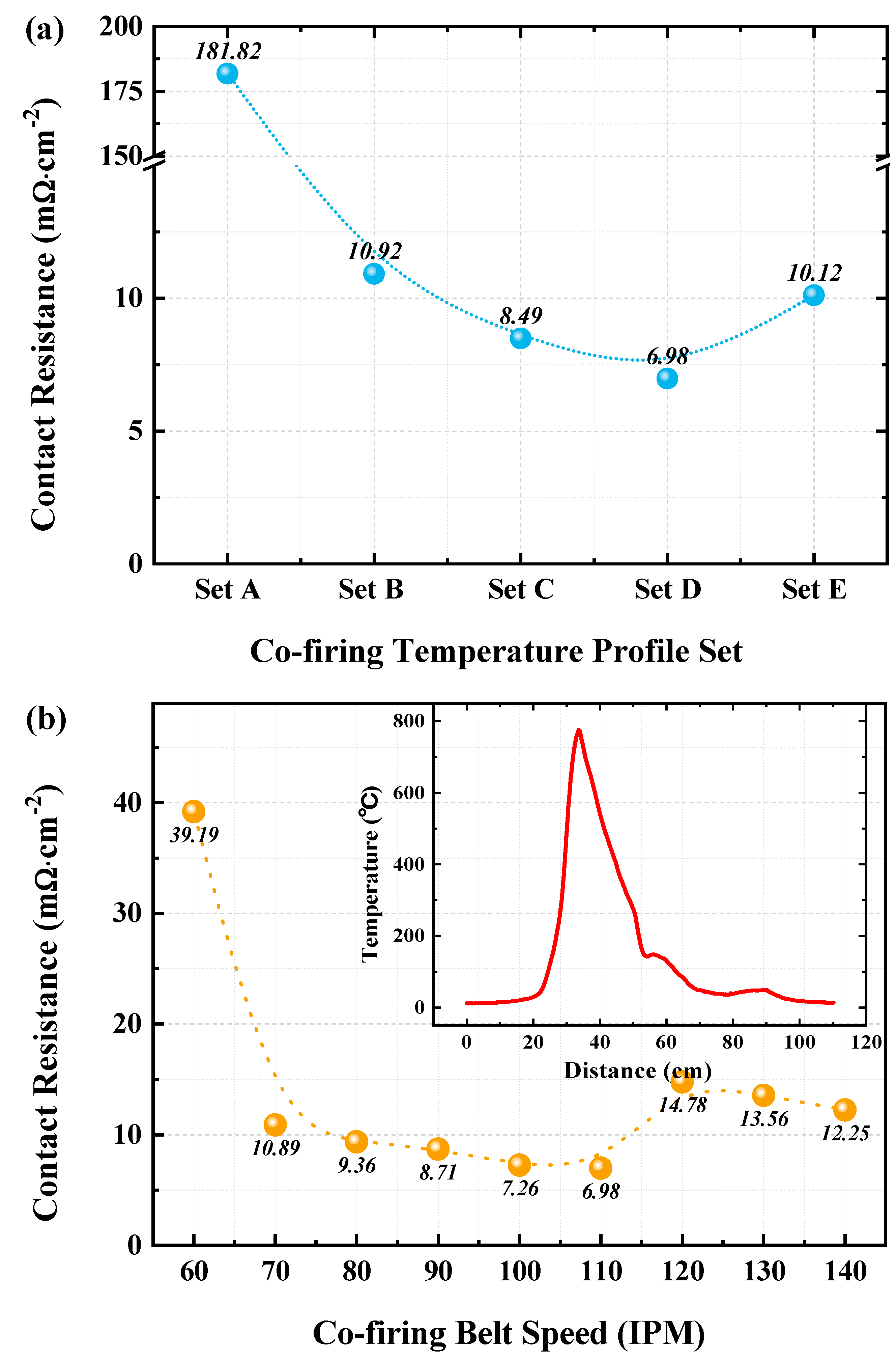
Figure 2 shows the variation in R
C with respect to the variation in the peak firing temperature of the fast-firing process. A sample with the same structure as that of the completed cell was fabricated; subsequently, the transmission line (TLM) method pattern was printed, and the Rc was measured. As
Figure 2a shows, the co-firing test group A had a very high R
C value, which can be attributed to the low peak firing temperature that was not sufficient to induce a reaction between the metal impurities in the screen-printed paste and the p+ diffused Si surface. Rc dramatically decreased from 181.82 mΩ∙cm
2 to 6.98 mΩ∙cm
2 for group D at a peak temperature of 865 °C. This revealed that an optimized co-firing temperature is required to initiate a reaction between metal impurities in screen-printing paste and Si atoms.
As the co-firing temperature for Set E was higher than that of Set D, R
C increased from 6.98 mΩ∙cm
2 to 10.12 mΩ∙cm
2. This increase in R
C may have been due to the variation in the reaction between metal impurities in the screen-printing paste and the Si surface caused by the over-fired electrode.
Figure 2b shows the variation in Rc with respect to the variation in the co-firing belt speed. The highest Rc value of 39.19 mΩ∙cm
2 was obtained at 60 ipm (inches per min). When the belt speed increased, the R
C value decreased to the lowest value of 6.98 mΩ∙cm
2. The excessive co-firing process time effect on the output characteristics of the c-Si solar cell owing to the denaturalization of the metals and other compositions of the electrode. Additionally, the Rc value increased for an increase in belt speed of 110 ipm because of insufficient composition reactions between diffused layer and electrode over the optimal co-firing speed. The actual firing profile for Set D with the lowest Rc was measured using a thermal profiling system (Datapaq Solar Tracker Thermal Profiling System, Fluke, Everett, Washington, DC, USA), and the results are shown in
Figure 2b. The measured peak temperature of set D was 775 °C.
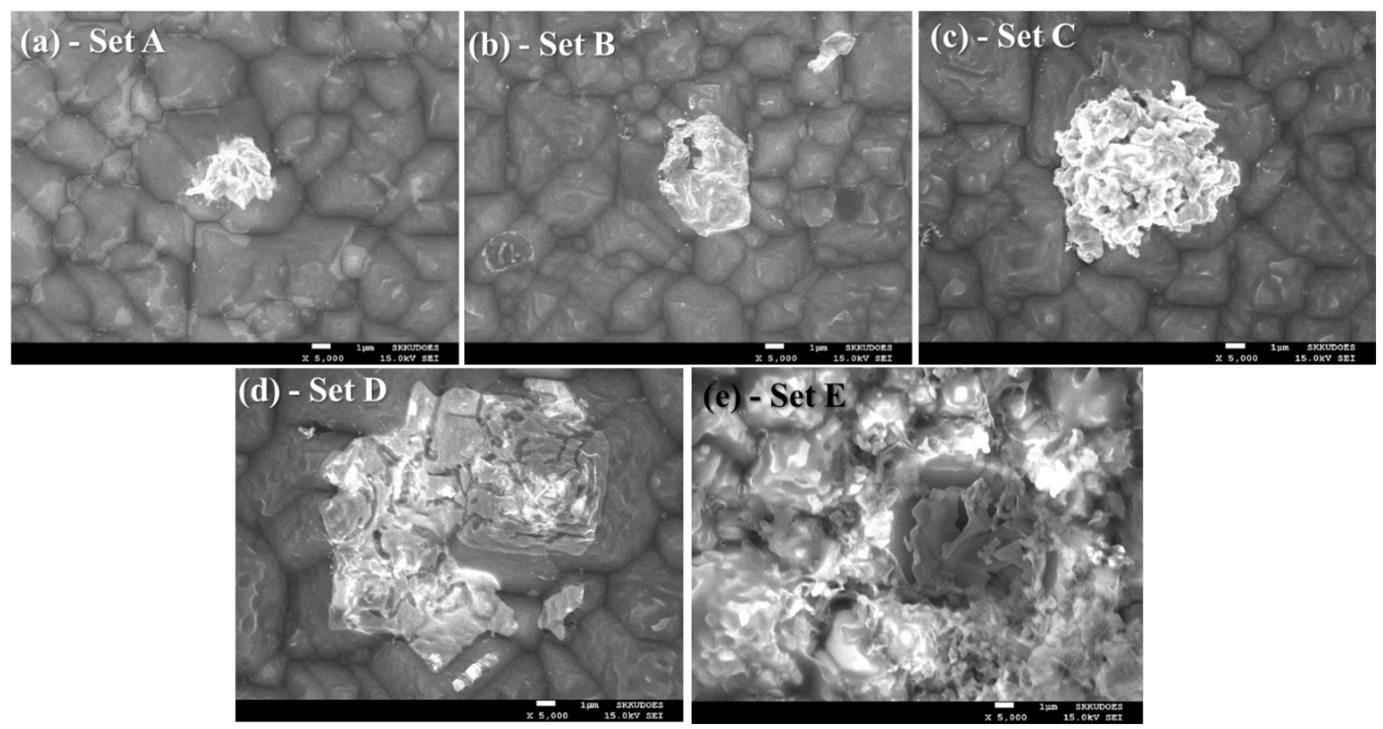
For further understanding of the characteristics of the contacts, the metal was etched, and the distribution of the crystallites was studied using SEM (
Figure 3). To etch the metal contacts, the cells were dipped in mixed acid, and the glass layer was removed using HF. The removal of the interfacial glass layer made viewing the metal crystallites grown emitter surface easier. For sets A and B, the remaining metal paste was observed, which could be because of the low firing temperature profile. The firing temperature increased, and the color of the metal paste changed. This indicated that the reaction between the metal paste and Si was effective. For set E, the color of the metal paste was darker, which might have been due to over-firing between Si and the metal paste.
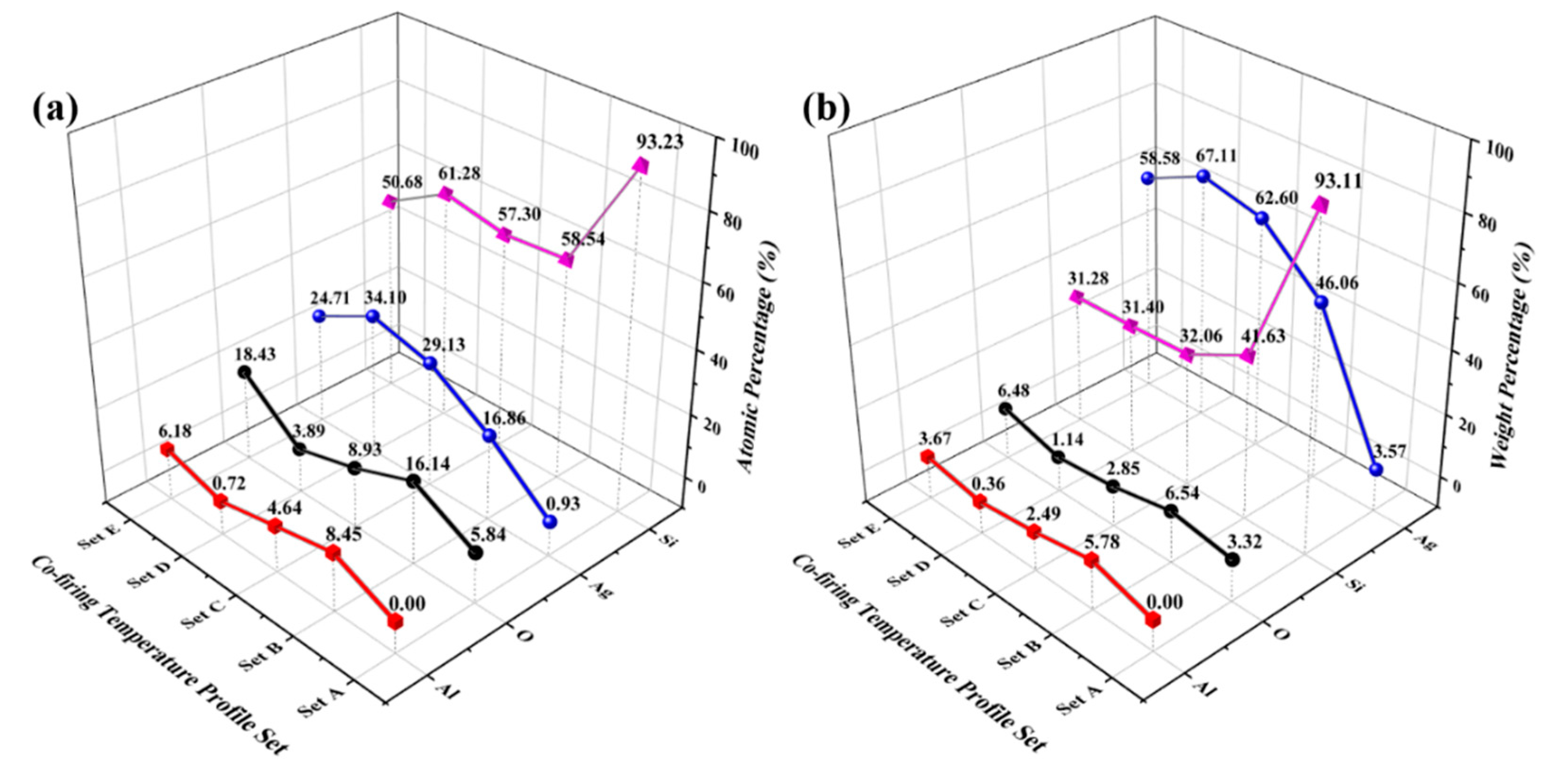
The at. wt % of the metals present on the surface were analyzed using EDS. By the electron beam of the SEM, each material emits its own specific X-ray during the sequence in which the electrons in the atom absorb and emit energy. The unique X-ray of each material inside the Ag–Al paste was collected by a detector and classified by intensity to perform a qualitative analysis (atomic/weight percentage) of the front electrode.
Figure 4 shows the at. wt % of O, Al, Si, and Ag with variation in the co-firing peak temperature. The EDS results indicated that the Ag content varied dramatically with the co-firing temperature. The at. wt % Si decreased as the co-firing temperature increased, revealing that glass frit and other metal atoms in the metal paste reacted with Si. For set A, as a special scenario, because the co-firing temperature was not sufficient to react with the Si substrate and Ag–Al Paste, most of the paste components disappeared in the HF solution, resulting in a low percentage of Ag and Al and a high proportion of Si. In contrast, the atomic and weight percentages of Ag increased from 16.86% to 34.10% and 46.06% to 67.11%, respectively, as the co-firing temperature increased. Ag atoms were bound to the Si surface after reaction with the glass frit in the metal paste. This determined the binding quality and electrode formation quality between the screen-printed metal paste and the p+ diffused surface of c-Si solar cells.
The at. wt % of Al exhibited a different trend compared with Ag and Si. This indicated that the Al content was bound to the p+ diffused surface with Ag in the Ag–Al metal paste as the co-firing temperature increased. When the co-firing temperature exceeded the optimized process window (>865 °C), Al remained in the electrode and surface because of over firing. The same behavior was observed in the weight percent analysis as the co-firing temperature varied. The difference in the percentage trend of Al in the EDS analysis results will be explained later in this section, but it can be considered as a difference in the contribution of Al to the formation of contact between Ag and Si. For set D, which had the best contact properties, the weight and atomic percentages of Al were the lowest (set A is excluded from this discussion). For set E, which had a higher temperature, Al melted rapidly in the eutectic phase and subsequently cooled, causing Al to escape and form additional voids. A similar pattern was observed in the Al-BSF of the PERC structure [
13]. The four-element analysis of the variation in the atomic and weight percentages resulted in contact characteristics between the p+ surface and screen-printed Ag–Al paste determined by the binding ratio of the weight and atomic percentages of Si, Ag, and Al.
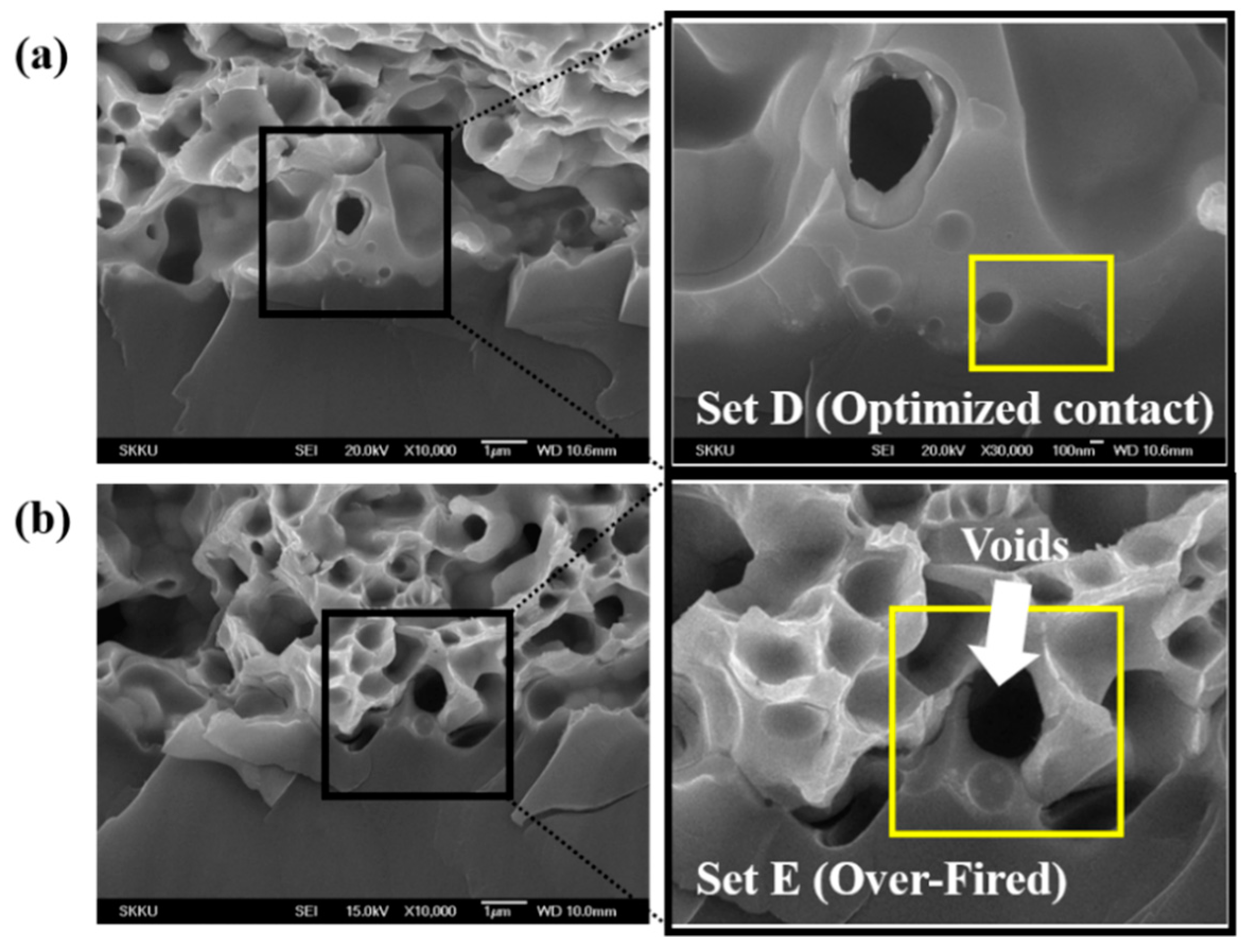
Figure 5 shows the SEM images of the alloy formation between the Ag–Al paste and the textured surface for the co-firing profile sets D and E. For the set E sample (
Figure 5b), the region between the textured surface and the metal alloy electrode had more voids owing to the over-fired co-firing temperature. A larger void between the pyramid surface and metal electrode decreased the contact characteristics, narrowing down the current path to the electrode. In contrast, for set D, no void region (
Figure 5a) occurred between the pyramid surface and metal alloy electrode region. This decreased the current loss.
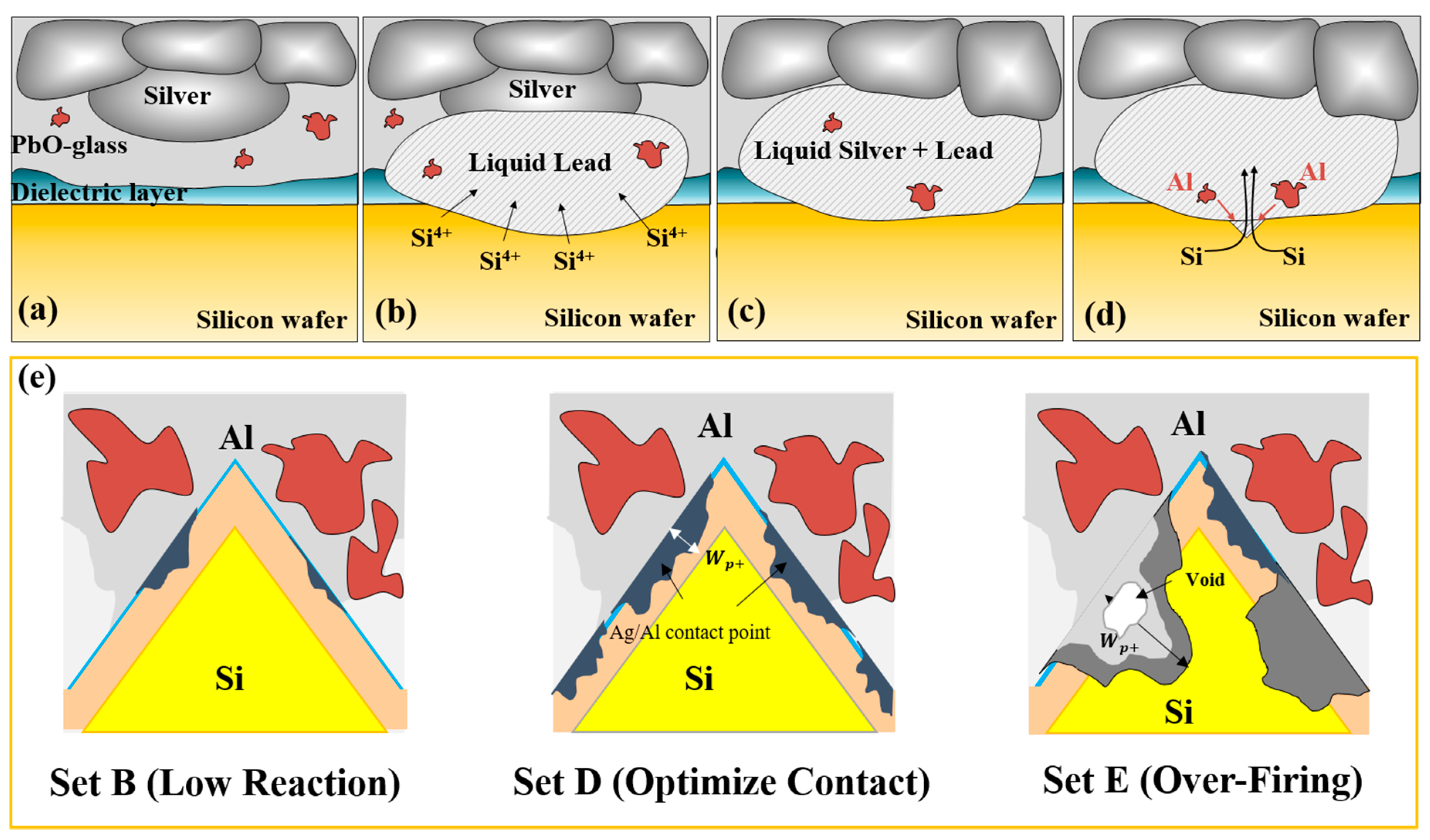
Figure 6 depicts the reaction diagram of the metal electrode paste and p+ (boron) diffused layer on the Si substrate during the co-firing process after the front and rear-side electrodes were screen-printed. The glass etched the antireflection coating, reduced the melting point of the metal, and promoted adhesion to Si during the firing cycle. The melted glass frits dissolved both Ag and Si. Ag was observed to dissolve in the glass frit when firing occurred. As the glass cooled, the Si regrew epitaxially and Ag crystallites grew into the Si surface from the glass. As described above, the reaction mechanism of the Ag–Al paste had the same pattern until the initial reaction with the general Ag-paste reaction of the p-type substrate excluding Al role in reaction phenomenon. In each firing temperature scenario, Al reacted differently from the p+ diffused and dielectric layers. For Set B, the width of Al and the p+ diffused layer Si alloy (
Wp+) was shallower than those in the other co-firing profiles because of insufficient reaction energy from thermal temperature. The relationship between W
p+, Al, and Si is expressed as [
14,
15,
16]
where
tAl is the as-deposited Al thickness,
ρAl and
ρSi are the densities of Al and Si, respectively,
F(
T) is the at. wt % of the molten phase of Si at the peak alloying temperature, and
F(
To) is the at. wt % of Si at the eutectic temperature (constant).
F(
T) and
F(
To) were obtained from the Al–Si phase diagram. Thus, the Al–Si atomic percentage determined
Wp+, and it had a role in the additional current path and locally electrical field similar to that of the Al–BSF layer in conventional p-type Si solar cells. Sets D and E exhibited optimized and over-fired contact phenomena after the co-firing process (
Figure 6e). In the overfired scenario, an excessive-
Wp+ layer was formed by a continuous reaction between Al and the p+ diffused layer during the high-temperature co-firing process. In addition, some voids were created at the boundary of the metal paste and the p+ diffused surface by the high reaction temperature and continuous reaction with Ag, Al, Si, and other materials in the electrode metal paste. Consequently, the p–n junction was locally damaged by the excessive-
Wp+ layer, decreasing the device conversion efficiency [
17].
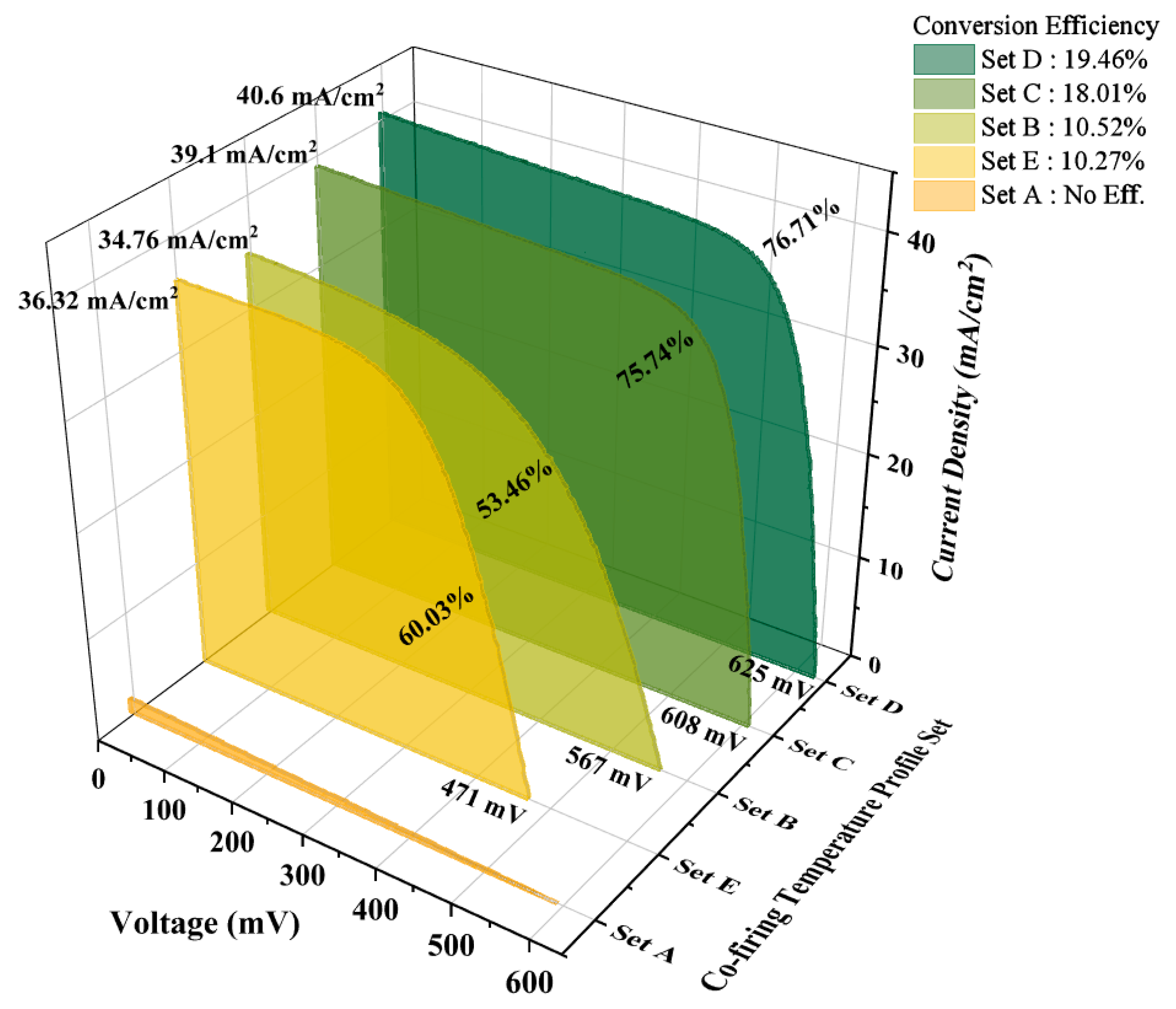
Figure 7 shows the LIV results of the solar cell fabricated using a co-firing temperature profile set. For set A, the conversion efficiency of the solar cell is not measured because the contact between the front electrode and the p+ diffused layer was not established, as indicated in the SEM/EDS analysis of the electrical properties of the contact. Based on the analysis of the contact properties, the co-firing profile of the other sets were observed to form a sufficient contact characteristic between the p+ diffused layer and the front electrode, unlike that of set A. Although the output characteristics of the solar cell differed, unlike for set A, the conversion efficiency was not measured to be approximately zero. In Set D, which exhibited the best characteristics in terms of Rc, the current density (J
SC), open-circuit voltage (V
OC), and fill factor (FF) exhibited the best characteristics among the remaining groups, with a conversion efficiency of 19.46%. Moreover, for set E, the Rc value exhibited good properties compared to set B; hence, the fill factor was 60.03%, which was 12% better than that of set B (53.46%). However, owing to the local damage of the p–n junction (as described in
Figure 5), an open-circuit voltage characteristic of 471 mV was observed, which was 17% lower than that of set B. The reason why it can be judged that the damage of the p–n junction by Al in the front paste affected the output characteristics of the solar cell, This is because the higher the peak temperature in the contact between the n+ diffused (phosphorus) layer on the back side and the Ag paste, the better it is in terms of contact resistance and fill factor [
18].
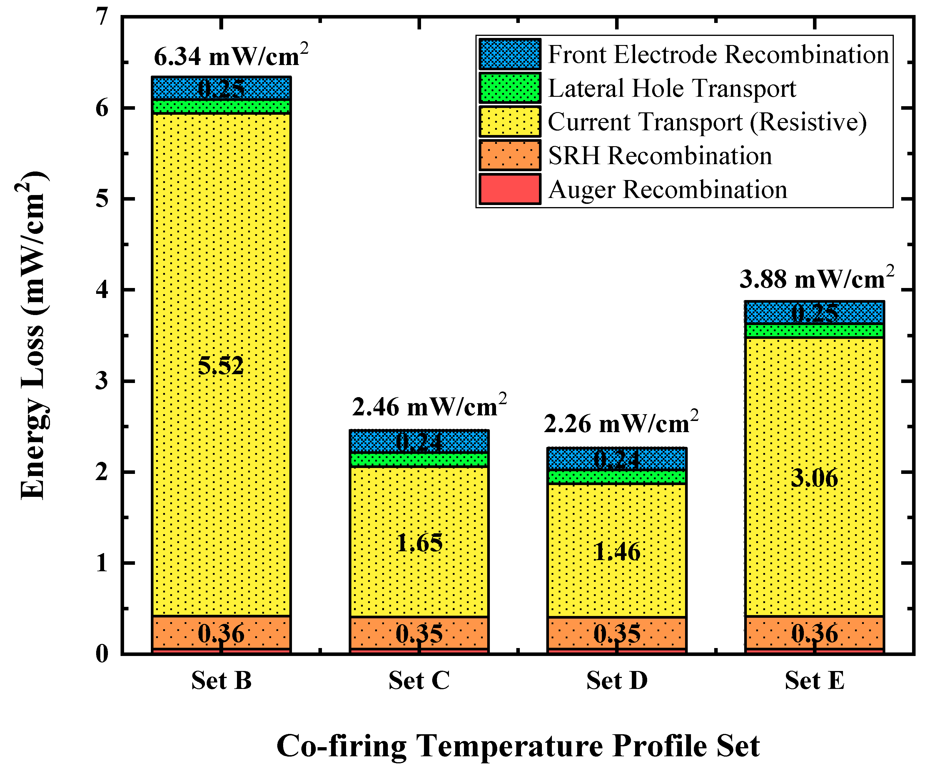
Figure 8 shows the loss analysis performed to determine which parameter decreased the output characteristics for the co-firing temperature profile sets B to E (set A was excluded from this analysis owing to low cell output properties in the LIV characteristics). The loss analysis was performed using the software Quokka 3 (March, Germany) technology computer-added design (TCAD) [
19,
20,
21]. The Rc values obtained from the results shown in
Figure 2 were input into the TCAD program.
Table 2 lists the detailed TCAD simulation parameters.
In this TCAD simulation analysis, five parameters were selected for the loss analysis: the “front electrode recombination”, which applied the characteristics of the front electrode loss such as the finger and busbar region; “lateral carrier transport”, which was based on the quality of the interface trap density of the front and rear passivation layer; “current transport loss (resistive)”, indicating the contact characteristics between the p+ diffused layer and front electrode; and the “SRH” and “Auger recombination” parameters, related to the recombination properties of the p+ diffused layer.
For set D, the current transport loss had a value of 1.464 mW/cm2, while the other groups had a value from 1.65 (set C) to 5.52 mW/cm2 (set B). Because the TCAD simulation was based on the same cell structure, most of the current transport loss could be estimated as the current transfer loss between the p+ diffused layer and the front electrode. In addition, the SRH and Auger recombinations, which represented recombination loss in the p+ diffused layer, exhibited the same loss percentage difference in all groups except set E. The ratio of current transport (resistive) loss accounted for approximately two-thirds of the total energy loss; therefore, it formed the major part of the key loss parameter.


