Abstract
In this research, simulations were performed to investigate the effects of carrier selective front contact (CSFC) layer and defect state of hydrogenated amorphous silicon passivation layer/n-type crystalline silicon interface in silicon heterojunction (SHJ) solar cells employing the Automat for Simulation of hetero-structure (AFORS-HET) simulation program. The results demonstrated the effects of band offset determined by band bending at the interface of the CSFC layer/passivation layer. In addition, the nc-SiOx: H CSFC layer not only reduces parasitic absorption loss but also has a tunneling effect and field effect passivation. Furthermore, it increased the selectivity of contact. In the experimental cell, nc-SiOx:H was used as the CSFC layer, where efficiency of the SHJ solar cell was 22.77%. Our investigation shows that if a SiOx layer passivation layer is used, the device can achieve efficiency up to 25.26%. This improvement in the cell is mainly due to the enhancement in open circuit voltage (Voc) because of lower interface defect density resulting from the SiOx passivation layer.
1. Introduction
Crystalline silicon (c-Si) solar cells dominate the global photovoltaic market, accounting for more than 90% of production [1,2]. Persistent efforts have been undertaken to achieve their theoretical efficiency threshold of 29.4% by improving the fundamental limiting factors. Recently, an efficiency level of 26.7% for a silicon heterojunction (SHJ) cell was reported by Kaneka corporation using the integrated back contact technique [3]. This result shows the potential of SHJ cell technology to achieve extremely high efficiency. Hence, this technology is expected to not only improve cell efficiency but also reduce manufacturing cost. The performance improvement of SHJ solar cells is dependent on reduction in the following: 1) carrier collection losses using thin wafer [4]; 2) surface recombination losses by surface passivation [5,6]; and 3) parasitic absorption loss of carrier selective front contact (CSFC) layers by controlling their thickness and using wide band-gap materials [7,8]. Interface defects and the optical parasitic absorption loss of the CSFC layers remain the key restrictions on the efficiency of SHJ solar cells.
Conventional SHJ solar cells are generally configured with front p-type hydrogenated amorphous silicon (p-a-Si:H) contact layers to collect better minority carriers [9]. However, due to high activation energy and the low band-gap of such front layers, a Schottky barrier is formed between the transparent conductive oxide (TCO) and p-a-Si:H layers [10,11]. Heavily doped p-layers can be used to reduce the Schottky barrier, but this causes parasitic absorption and increased carrier recombination. Hence, a rear emitter SHJ solar cell (RE-SHJ) with a p-layer located on the rear side has been analyzed [12]. Conventional RE-SHJ solar cells use doped a-Si:H material as both the front and back carrier selective contact layers. The internal electric field is formed according to the doping concentration of these doped layers and, as a result, the carriers are separated and collected. As the doping concentration increases, doping-induced defects also increase, which limits the efficiency of the device. Additionally, the a-Si:H materials reduce transmittance owing to the inherent low band-gap. A wide-gap hydrogenated nanocrystalline silicon oxide (nc-SiOx:H) layer, which compensates for the disadvantages of a-Si:H [13], is a suitable alternative for the efficiency improvement of RE-SHJ devices. Compared with a-Si:H, nc-SiOx:H has a low absorption coefficient in the short wavelength region, as well as excellent conduction properties owing to the crystalline phase and quantum confinement effects [14]. In this paper, we present the numerical simulation of RE-SHJ cells using Automat for simulation hetero-structures (AFORS-HET) software. The influence of a-Si:H and silicon oxide materials functionalized as passivation and CSFC layers for the RE-SHJ cells is discussed under experimental and simulation results. The simulation is performed to identify the essential factors for enhancing the efficiency of the device. A numerical simulation is performed in conjunction with experimental data (absorption coefficient, extinction coefficient and optical band gap for each layer) to evaluate the conditions required to increase the efficiency of the solar cells.
2. Materials and Methods
2.1. Experimental Methods
In the device fabrication, a Czochralski (CZ)-grown n-type silicon wafer (148 µm thickness and 1.5 Ωcm resistivity) was used. The surface texturing was performed using sodium hydroxide (8% NaOH) solution. Radio Corporation of America (RCA) standard cleaning was used to remove the surface impurities from the texture wafers and was applied in two stages: standard cleaning 1 and 2. Subsequently, a thin a-Si:H passivation layer was prepared on both interfaces of the Si-wafer. The doped n-type layer was deposited at the front side, and the p-type layer was deposited at the rear. These layers were deposited by employing a standard plasma-enhanced chemical vapor deposition system. The front and back TCO layers were deposited using the radio frequency (RF) sputtering system, which requires Ar feed gas and approximately 200 °C substrate heating during deposition. Additionally, screen printing with Ag paste was used for the front metal grid and back contact electrodes. The RE-SHJ cell structure consisted of front electrode/TCO/n-type CSFC layer/a-Si:H passivation layer/c-Si wafer/a-Si:H passivation layer/p-layer emitter/TCO/back electrode, as shown in Figure 1.
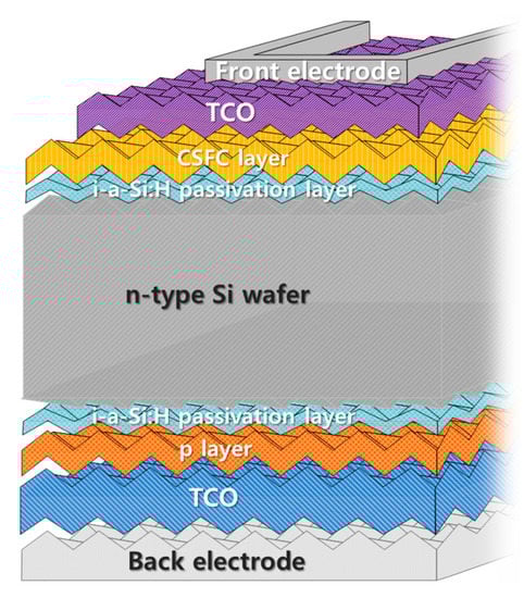
Figure 1.
Schematic structure of a heterojunction solar cell.
For the wafer surface passivation with SiOx layers, the SiOx passivation layer was formed by varying the pressure of CO2 plasma post-treatment from 1600 to 2200 mTorr on the a-Si/Si-wafer interface. The minority carrier lifetime (τeff) was examined using quasi-steady-state photo conductance (QSSPC, WCT-120). For measuring spectroscopic ellipsometry (SE) and X-ray photoelectron spectroscopy, a <100> n-type CZ Si wafer (1–10 Ωcm) with one-side polished was used. The thickness, refractive index, absorption coefficient and optical bandgap were measured by SE (VASE, J. A. Woollam) in the 240 to 1700 nm wavelength range. An X-ray photoelectron spectroscopy (XPS, K-Alpha, Thermo Scientific) system was utilized to estimate the chemical composition using Al Kα radiation.
2.2. Modeling of HIT Solar Cells
The recombination in the semiconductor was calculated using Shockley–Read–Hall statistics [15]. The defect state was investigated at the passivation layer/Si-wafer interface by varying the defect density in the range of 1 × 10¹⁰ to 1 × 1014 cm−2eV−1. The illuminated current–voltage characteristics were measured at AM 1.5G (100 mW/cm2). The Gaussian defect distribution was utilized to describe the band tail states of a-Si:H and nc-SiOx:H layers in both valence and conduction band. Due to the n-type c-Si substrate, oxide energy levels with an average defect density of 1 × 1011 cm−2eV−1 were settled at 0.53 eV from the conduction band. The simulated parameters are listed in Table 1 for all layers. The RE- SHJ solar cell with n-a-Si:H CSFC layer (Figure 2a) consisted of front electrode/TCO/n-a-Si:H CSFC layer/i-a-Si:H passivation layer/n-type c-Si wafer/i-a-Si:H passivation layer/p-a-Si:H layer/TCO/back electrode. The RE-SHJ solar cell with nc-a-SiOx:H CSFC layer (Figure 2b) consisted of front electrode/TCO/n-a-Si:H CSFC layer/i-a-Si:H passivation layer/n-type c-Si wafer/i-a-Si:H passivation layer/p-nc-SiOx:H layer/TCO/back electrode.

Table 1.
Material parameter values for SHJ solar cell simulation.
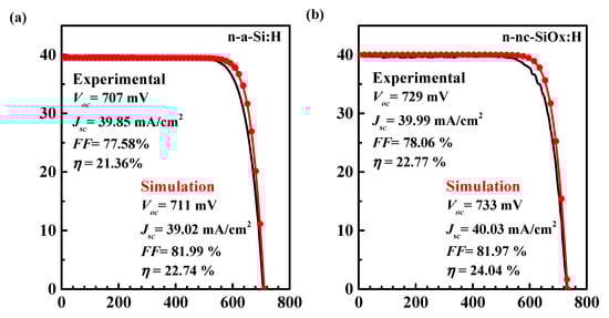
Figure 2.
J-V curve characteristics of rear emitter silicon heterojunction (SHJ) solar cells with different carrier selective front contact (CSFC) layers: (a) a-Si:H; (b) a-SiOx:H. Experimental results are indicated by the continuous line, while the simulation results are indicated by the symbol.
3. Results and Discussion
3.1. Numerical Simulation of HIT Solar Cell
The SHJ solar cells use a-Si:H materials as the passivation and carrier selective contact layers at both sides for separate electron-hole pairs. The conventional SHJ solar cell uses the p-a-Si:H layer as a CSFC layer. This layer absorbs light in the short wavelength region and has low conductivity, which leads to parasitic absorption losses. The simulation of the rear emitter with various CSFC layers and interface defect states was investigated. The simulations were performed using optical parameters of layers, including extinction coefficient (k), refractive index (n), and optical bandgap (Eg) obtained via ellipsometry, as well as electrical parameter measurements. The J-V curve characteristics of the RE-SHJ cells with different CSFC layers were compared to that of real cells, as shown in Figure 3. It can be observed that the characteristics of the simulated results are very similar to that of the real cell; for example, while fill factor (FF) depicted a higher deviation, the other parameters were very close to those of the real cells. The nc-SiOx:H CSFC layer achieved a conversion efficiency of 24.04%. The decrease in parasitic absorption of the wide-gap nc-SiOx:H CSFC layer assisted the increase in short circuit current density (Jsc). The increase in efficiency of the RE-SHJ cell using the nc-SiOx:H CSFC layer is explained through the band diagram, electric field and generation/recombination rate.
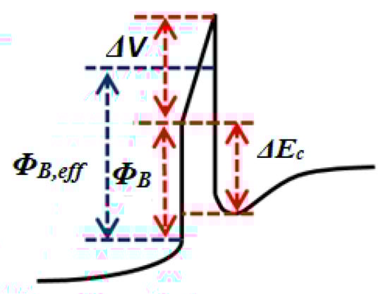
Figure 3.
Construction of an effective tunnel barrier by considering the potential drop through the passivation layer.
Figure 3 can be represented by the following equation:
where ϕB,eff is the effective barrier height and ΔV is the electrostatic potential drop [15]. ϕB,eff is 0.038 eV and 0.073 eV with a-Si:H CSFC and nc-SiOx:H CSFC layer, respectively.
Figure 4 shows the band diagram in the equilibrium condition for different CSFC layers. To observe the comparative change in the band structure, the band offsets at the valence (ΔEv) and conduction (ΔEc) bands of the RE-SHJ with various CSFC layers are depicted in Figure 4b,c, respectively. The values of ΔEc are 0.082 eV and 0.046 eV for Figure 4b,c, respectively. The smaller value of ΔEc yielded higher electron collection. It can be observed that the nc-SiOx:H CSFC layer created a barrier for tunneling the electrons between the CSFC layer and n-type c-Si wafer. When using the nc-SiOx:H CSFC layer, the barrier is considered triangular, as shown in Figure 4.
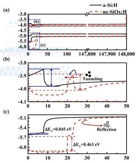
Figure 4.
Band diagram of the rear emitter SHJ solar cell: (a) band diagram; (b) conduction band; (c) valence band with different CSFC layers.
The increase in ΔEv acts as a hole reflector at the interface. The nc-SiOx:H CSFC layer acts as an effective hole reflector. This leads to reduction in interface recombination. As a result, the nc-SiOx:H CSFC layer-enhanced Voc and Jsc are approximately 0.733 V and 40.03 mA/cm2, respectively. To assess the effect of the nc-SiOx:H CSFC layer, the electric field and generation/recombination rate were investigated using the numerical simulation as depicted in Figure 5. The electric field was 7.69 × 10⁸ V/cm for the cell using the a-Si:H as passivation and the CSFC layer. For the cell using the nc-SiOx:H CSFC layer, the electric field was increased to 2.78 × 10⁹ V/cm between the passivation and the nc-SiOx:H CSFC layers. The high electric field with nc-SiOx CSFC layer is due to high band bending, as depicted in Figure 4 [16]. The nc-SiOx:H CSFC layer can increase Voc as well as lead to field effect passivation. As shown in Figure 5, the interface recombination rate increased over 1 × 10²¹ m−3S−1 at the n-a-Si:H CSFC /a-Si:H passivation interface but drastically reduced under 1 × 10¹⁶ m−3S−1 between nc-SiOx:H CSFC layer/a-Si:H passivation layer.
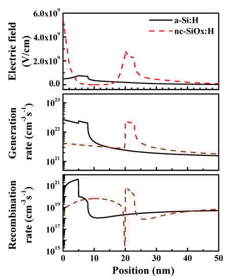
Figure 5.
Influence of the CSFC layer on electric field, generation rate and recombination rate.
The field effect passivation causes decrease of recombination rate at the interface. The influence of the interface defect state of the RE-SHJ solar cell was investigated by simulation. Figure 6a shows the cell parameters as a function of the interface defect density (Dit) for different CSFC layers of RE-SHJ cells. When Dit was increased from 5 × 108 cm−2 to 1 × 1013 cm−2, the cell efficiency and Jsc decreased slightly at first, and then became almost zero. These results indicate that Dit is required to be lower than 2 × 1010 cm−2 and 8 × 1010 cm−2 in case of using a-Si:H and nc-SiOx:H layers, respectively, to obtain a Voc over 700 mV. The Voc is affected by interface recombination of the SHJ solar cell as follows [17]:
where q is the elementary charge, ϕc is the effective barrier height in crystalline silicon, A is the ideality factor, k is the Boltzmann constant, T is the temperature, Sit is the interface recombination velocity, and Nv is the effective valence band density. The interface defect state affects surface recombination. The high Dit leads to increase of Sit, and therefore decreased Voc. The interface defect state affects the quasi Fermi level and band bending. In Figure 6b, the band diagram of a SHJ solar cell using a-Si:H CSFC layer is shown with different Dit. When Dit increases, the hole quasi-Fermi energy (EFp) shifts to a high energy level, which can result in a decrease of Voc. EFp can be described by the-one dimensional continuity equation as [18]:
where Ev is the valence band energy, χ is the electron affinity, φ(x,t) is the local electric potential in the semiconductor layers and Eg is the bandgap. The value of EFp is increased due to the decrease in electric potential and an increase in Nv. The high Dit leads to a decrease in band bending and hence a decrease in electric potential. Additionally, it causes an improvement in the majority carrier concentration. The nc-SiOx:H CSFC layer also follows the same trend as shown in Figure 6b. In contrast, the nc-SiOx:H CSFC layer shows lower performance degradation even with 8 × 1010 cm−2 due to the tunneling effect and field effect passivation of the CSFC layer/a-Si:H passivation layer at the interface.
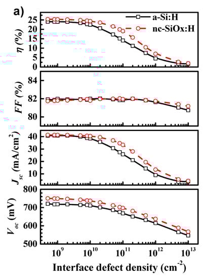
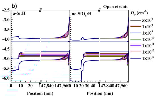
Figure 6.
Schemes of rear emitter SHJ solar cells including: (a) The Voc, Jsc, FF and η cell parameters as a function of interface defect density and (b) band diagrams with different interface defect density of a-Si:H CSFC (left) and nc-SiOx:H CSFC (right) layer.
3.2. Hydrogenated Silicon Oxide Passivation Layer
The results in the previous section suggest that a low Dit can enhance Voc and thus efficiency of the SHJ solar cell. A low Dit can lead to high band bending at the a-Si:H/c-Si interface, which increases the Voc of the cell. A further low Dit can result from a hydrogenated silicon oxide (a-SiOx:H) passivation layer formed through CO2 plasma post-treatment. The Figure 7 shows the structural and optical properties of the a-SiOx:H layers under CO2 plasma post-treatment.
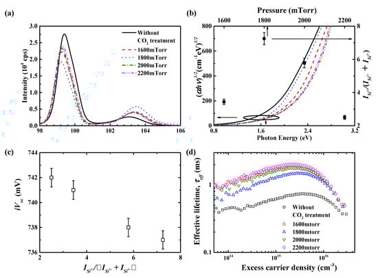
Figure 7.
Structural and optical properties of a-SiOx:H layers under different CO2 plasma post-treatment including: (a) Si 2p core-level XPS spectra of a-Si:H and a-SiOx:H different CO2 plasma post-treatment pressure, (b) ISi1+/(ISi2++ISi3+) ratio derived from the XPS spectra as a function of plasma post-treatment pressure and optical band gap of the a-Si:H and a-SiOx:H plotted as a function of photon energy, (c) iVoc with respect to the ISi1+/(ISi2++ISi3+) ratio, and (d) effective carrier lifetime measured by quasi-steady-state photo conductance (QSSPC) as a function of the treatment pressure.
Chemical composition of the a-Si:H and a-SiOx:H layers was confirmed by employing XPS analysis, as shown in Figure 7a. After CO2 plasma post-treatment, the pure Si peak decreased and the SiO2 peak increased with the increase of treatment pressure. Increasing the treatment pressure led to the formation of oxygen-rich silicon oxide states. The absorption coefficient of the a-SiOx:H layer with different CO2 plasma treatment pressures were investigated using SE analysis, as shown in Figure 7b. The optical band gaps were determined through absorption coefficients. At higher CO2 plasma treatment pressure, the a-SiOx:H layer exhibited a high optical band gap, owing to the oxygen-rich components. The XPS spectrum demonstrated the increase in the formation of Si1+, Si2+, Si3+, and Si4+ peaks. The XPS spectra were deconvoluted into six doublets, Si 2p3/2 (93.90 eV), Si 2P1/2 (99.90 eV), Si2O (100.15 eV), SiO (101.05 eV), Si2O3 (101.80 eV) and SiO2 (103 eV), as shown in Figure 8. In Figure 7b, the oxide state ratio (ISi1+/(ISi2++ISi3+)) is presented for the different working pressures during CO2 plasma post-treatment. The oxide state ratio increased to a treatment pressure of 1800 mTorr and decreased above 1800 mTorr. The oxygen-rich components (Si2+ and Si3+) further increased at a higher treatment pressure. To determine the optimal oxide state for high Voc, as shown in Figure 7c, the effect of the oxide state ratio on iVoc was investigated. The optimum value of iVoc was 742 mV when the oxide state ratio was 2.5. The surface passivation properties of the a-SiOx:H layer on textured n-type c-Si wafer was investigated. As a function of excess carrier density, the plot of τeff with a variation of plasma treatment pressure is shown in Figure 7d. After CO2 plasma treatment, τeff increased with the increase in treatment pressure. At low injection levels of carrier density, the improvement of τeff can be explained through field effect passivation. It can be observed that a-SiOx:H increased ΔEv at the a-SiOx:H/c-Si interface. This phenomenon leads to enhancement of the reflection of minority carriers (hole) at the interface, which helps in low interface recombination.
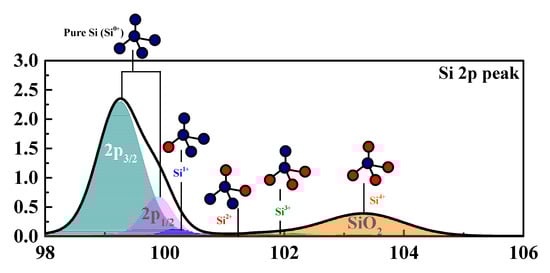
Figure 8.
Peak fit for an a-SiOx:H layer XPS spectra, showing the different oxidation states.
To confirm the cell results, we simulated the RE-SHJ solar cells using a-SiOx:H passivation layer. In Figure 9, the J-V parameters are presented as a function of the various working pressures for the CO2 plasma post-treatment. As depicted in Figure 9, the efficiency increases with CO2 plasma post-treatment. The optical band gap of the a-SiOx:H layer increased with CO2 plasma treatment. This optical band gap created a higher ΔEv at the a-SiOx:H/c-Si interface, which may have assisted in hole reflection and decreased recombination. We investigated the effect of using a-SiOx:H passivation layer. This is because the a-SiOx:H has a wider band gap and good passivation properties. The result shows that such an increase of the Voc is feasible by employing an appropriate a-SiOx:H as the passivation layer.
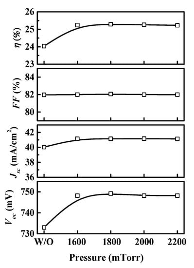
Figure 9.
Estimated J-V parameters of rear emitter HIT cells as a function of CO2 plasma post-treatment.
4. Conclusions
In this paper, the impact of various CSFC layers and interface defect densities on the efficiency of RE-SHJ solar cells was discussed through simulations and experiments. To compare the effect of the various CSFC layers, simulations were performed using a-Si:H and nc-SiOx:H CSFC materials. Using a nc-SiOx:H CSFC layer results in the decreased parasitic absorption and recombination loss through field effect passivation, thus enhancing RE-SHJ cell efficiency. The output parameters of RE-SHJ solar cell, such as Voc = 733 mV, Jsc = 40.03 mA/cm2, FF = 81.97% and η = 24.04%, were obtained using a nc-SiOx:H CSFC layer. The increase in interface defect states resulted in a decrease in band bending and a shift in EFp to high energy and hence a reduction in Voc. Finally, the nc-SiOx:H CSFC layer has better performance in the same interface defect state than the a-Si:H CSFC layer. This improvement is attributed to the tunneling effect and field effect passivation when using the nc-SiOx:H CSFC layer. To improve the surface passivation quality of the RE-SHJ cell, the a-SiOx:H layer was used as the passivation layer. The Voc increased due to the decrease of the recombination rate at the interface. This investigation suggests that a suitable a-SiOx:H passivation layer can significantly improve the Voc and efficiency of SHJ solar cells.
Author Contributions
S.L. is the main author. S.L. and D.P.P. carried out the investigations and undertook the simulation and data analysis. Y.K., E.-C.C. and J.Y. supervised the project as was also responsible for funding acquisition. S.L. and J.P. were responsible for the writing—original draft preparation while all authors were involved in writing—review and editing. All authors have read and agreed to the published version of the manuscript.
Funding
This work was supported by the Korea Institute of Energy Technology Evaluation and Planning (KETEP) and the Ministry of Trade, Industry and Energy (MOTIE) of the Republic of Korea (No. 20203030010310) and the National Research Foundation of Korea(NRF) funded by the Korea government (MSIT) (NRF-2019R1A2C1009126).
Conflicts of Interest
The authors declare no conflict of interest.
References
- Zheng, C.; Kammen, D.M. An innovation-focused roadmap for a sustainable global photovoltaic industry. Energy Policy 2014, 67, 159–169. [Google Scholar] [CrossRef]
- Battaglia, C.; Cuevas, A.; De Wolf, S. High-efficiency crystalline silicon solar cells: Status and perspectives. Energy Environ. Sci. 2016, 9, 1552–1576. [Google Scholar] [CrossRef]
- Yoshikawa, K.; Kawasaki, H.; Yoshida, W.; Irie, T.; Konishi, K.; Nakano, K.; Uto, T.; Adachi, D.; Kanematsu, M.; Uzu, H.; et al. Silicon heterojunction solar cell with interdigitated back contacts for a photoconversion efficiency over 26%. Nat. Energy 2017, 2, 17032. [Google Scholar] [CrossRef]
- Tohoda, S.; Fujishima, D.; Yano, A.; Ogane, A.; Matsuyama, K.; Nakamura, Y.; Tokuoka, N.; Kanno, H.; Kinoshita, T.; Sakata, H.; et al. Future directions for higher-efficiency HIT solar cells using a Thin Silicon Wafer. J. Non-Cryst. Solids 2012, 358, 2219–2222. [Google Scholar] [CrossRef]
- Deligiannis, D.; Van Vliet, J.; Vasudevan, R.; Van Swaaij, R.A.C.M.M.; Zeman, M. Passivation mechanism in silicon heterojunction solar cells with intrinsic hydrogenated amorphous silicon oxide layers. J. Appl. Phys. 2017, 121, 085306. [Google Scholar] [CrossRef]
- Liu, W.; Zhang, L.; Cong, S.; Chen, R.; Wu, Z.; Meng, F.; Shi, Q.; Liu, Z. Controllable a-Si:H/c-Si interface passivation by residual SiH4 molecules in H2 plasma. Sol. Energy Mater. Sol. Cells 2018, 174, 233–239. [Google Scholar] [CrossRef]
- Holman, Z.C.; Descoeudres, A.; Barraud, L.; Fernandez, F.Z.; Seif, J.P.; De Wolf, S.; Ballif, C. Current losses at the front of silicon heterojunction solar cells. IEEE J. Photovolt. 2012, 2, 7–15. [Google Scholar] [CrossRef]
- Mazzarella, L.; Kirner, S.; Stannowski, B.; Korte, L.; Rech, B.; Schlatmann, R. P-type microcrystalline silicon oxide emitter for silicon heterojunction solar cells allowing current densities above 40 mA/cm2. Appl. Phys. Lett. 2015, 106, 023902. [Google Scholar] [CrossRef]
- Taguchi, M.; Terakawa, A.; Maruyama, E.; Tanaka, M. Obtaining a higher voc in HIT cells. Prog. Photovolt. Res. Appl. 2005, 13, 481–488. [Google Scholar] [CrossRef]
- Bivour, M.; Schröer, S.; Hermle, M. Numerical analysis of electrical TCO/a-Si:H(p) contact properties for silicon heterojunction solar cells. Energy Procedia 2013, 38, 658–669. [Google Scholar] [CrossRef]
- Varache, R.; Kleider, J.P.; Gueunier-Farret, M.E.; Korte, L. Silicon heterojunction solar cells: Optimization of emitter and contact properties from analytical calculation and numerical simulation. Mater. Sci. Eng. B Solid-State Mater. Adv. Technol. 2013, 178, 593–598. [Google Scholar] [CrossRef]
- Bivour, M.; Schröer, S.; Hermle, M.; Glunz, S.W. Silicon heterojunction rear emitter solar cells: Less restrictions on the optoelectrical properties of front side TCOs. Sol. Energy Mater. Sol. Cells 2014, 122, 120–129. [Google Scholar] [CrossRef]
- Mazzarella, L.; Morales-Vilches, A.B.; Korte, L.; Schlatmann, R.; Stannowski, B. Ultra-thin nanocrystalline n-type silicon oxide front contact layers for rear-emitter silicon heterojunction solar cells. Sol. Energy Mater. Sol. Cells 2018, 179, 386–391. [Google Scholar] [CrossRef]
- Richter, A.; Smirnov, V.; Lambertz, A.; Nomoto, K.; Welter, K.; Ding, K. Versatility of doped nanocrystalline silicon oxide for applications in silicon thin-film and heterojunction solar cells. Sol. Energy Mater. Sol. Cells 2018, 174, 196–201. [Google Scholar] [CrossRef]
- Varache, R.; Leendertz, C.; Gueunier-Farret, M.E.; Haschke, J.; Muñoz, D.; Korte, L. Investigation of selective junctions using a newly developed tunnel current model for solar cell applications. Sol. Energy Mater. Sol. Cells 2015, 141, 14–23. [Google Scholar] [CrossRef]
- Gudovskikh, A.S.; Ibrahim, S.; Kleider, J.P.; Damon-Lacoste, J.; Roca i Cabarrocas, P.; Veschetti, Y.; Ribeyron, P.J. Determination of band offsets in a-Si:H/c-Si heterojunctions from capacitance-voltage measurements: Capabilities and limits. Thin Solid Films 2007, 515, 7481–7485. [Google Scholar] [CrossRef]
- Dao, V.A.; Heo, J.; Choi, H.; Kim, Y.; Park, S.; Jung, S.; Lakshminarayan, N.; Yi, J. Simulation and study of the influence of the buffer intrinsic layer, back-surface field, densities of interface defects, resistivity of p-type silicon substrate and transparent conductive oxide on heterojunction with intrinsic thin-layer (HIT) solar cell. Sol. Energy 2010, 84, 777–783. [Google Scholar] [CrossRef]
- Bashiri, H.; Karami, M.A.; Mohammadnejad, S. A theoretical investigation of quantum confinement effects in heterojunction silicon solar cells. Indian J. Phys. 2018, 92, 349–356. [Google Scholar] [CrossRef]
© 2020 by the authors. Licensee MDPI, Basel, Switzerland. This article is an open access article distributed under the terms and conditions of the Creative Commons Attribution (CC BY) license (http://creativecommons.org/licenses/by/4.0/).