1. Introduction
Nowadays, multilevel inverters (MLIs) are widely used, since they offer improved output waveforms, smaller grid filter size, lower total harmonic distortion (THD), and reduced electromagnetic interference (EMI), compared to their two-level inverter counterparts [
1,
2,
3,
4,
5,
6]. In particular, MLIs are particularly suitable for medium- and high-voltage applications for both single- and three-phase systems, thanks to the possibility to work with high-voltage levels by adopting low-voltage-rated devices.
The basic multilevel converter topologies are cascade H-bridge (CHB), neutral-point-clamped (NPC), flying capacitor (FC), and modular multilevel converter (MMC) [
5,
6]. These kinds of converters are also adopted in photovoltaic applications due to the aforementioned advantages.
Many recently published papers deal with the estimation of voltage and current THD in multilevel inverters. In most of the cases, they are based on voltage frequency spectra numerical calculations/measurements (fast Fourier transform, FFT). The scientific community has shown a significant interest in voltage and current THD analyses for both multilevel pulse width modulation (PWM) and staircase modulation over the past years. Analytical solutions for the voltage THD of multilevel PWM single- and three-phase inverters were obtained in [
7] in asymptotic approximation (high switching-to-fundamental frequency ratio). Experimental tests have been carried out in [
8] to verify the calculation and analytical developments of voltage and current THDs in the case of three-, five-, and seven-level single-phase PWM inverters.
Cascade H-Bridge converter is a mature multilevel topology adopted for different applications with multiple DC sources [
1,
2,
3,
4].
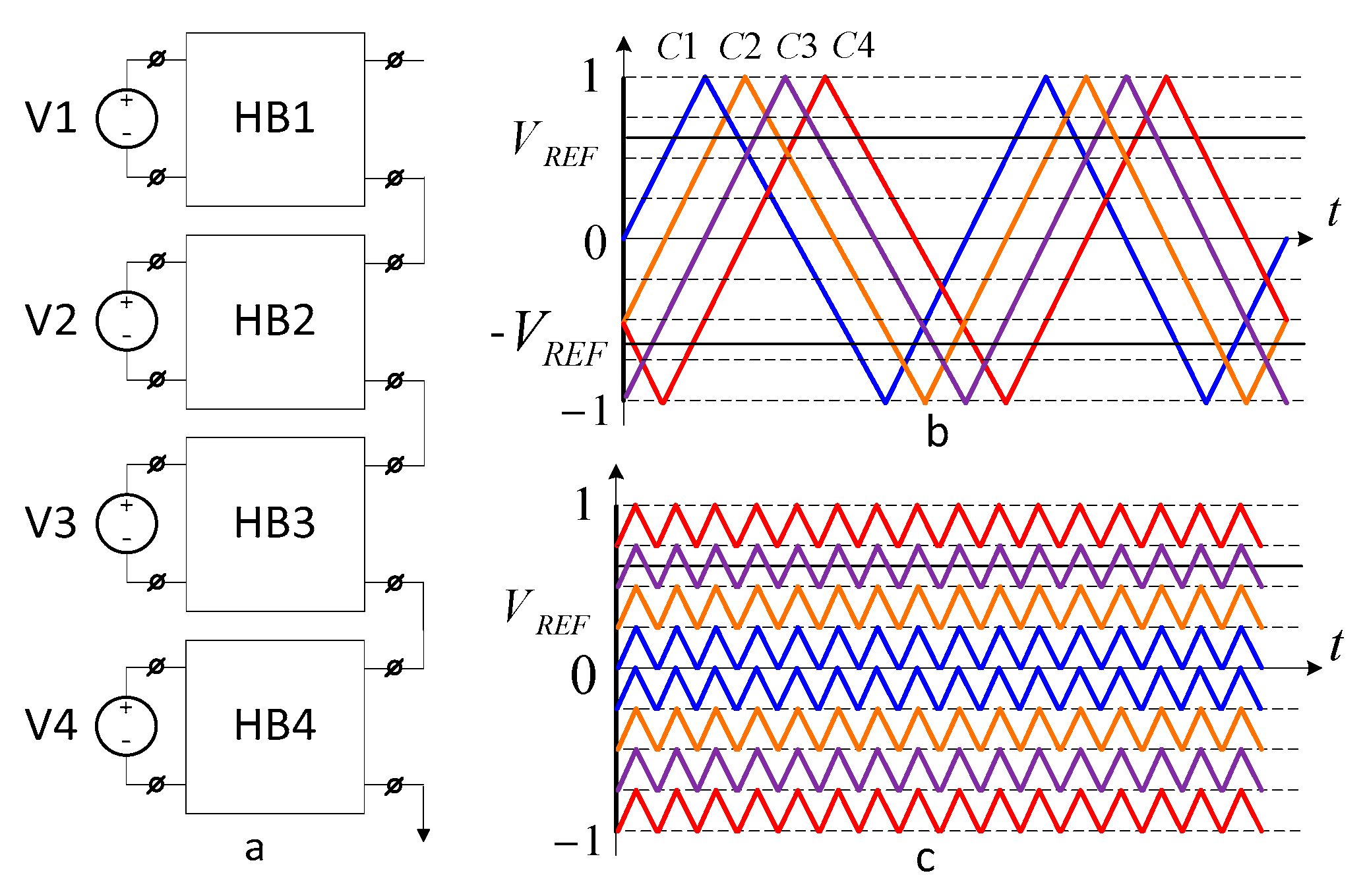
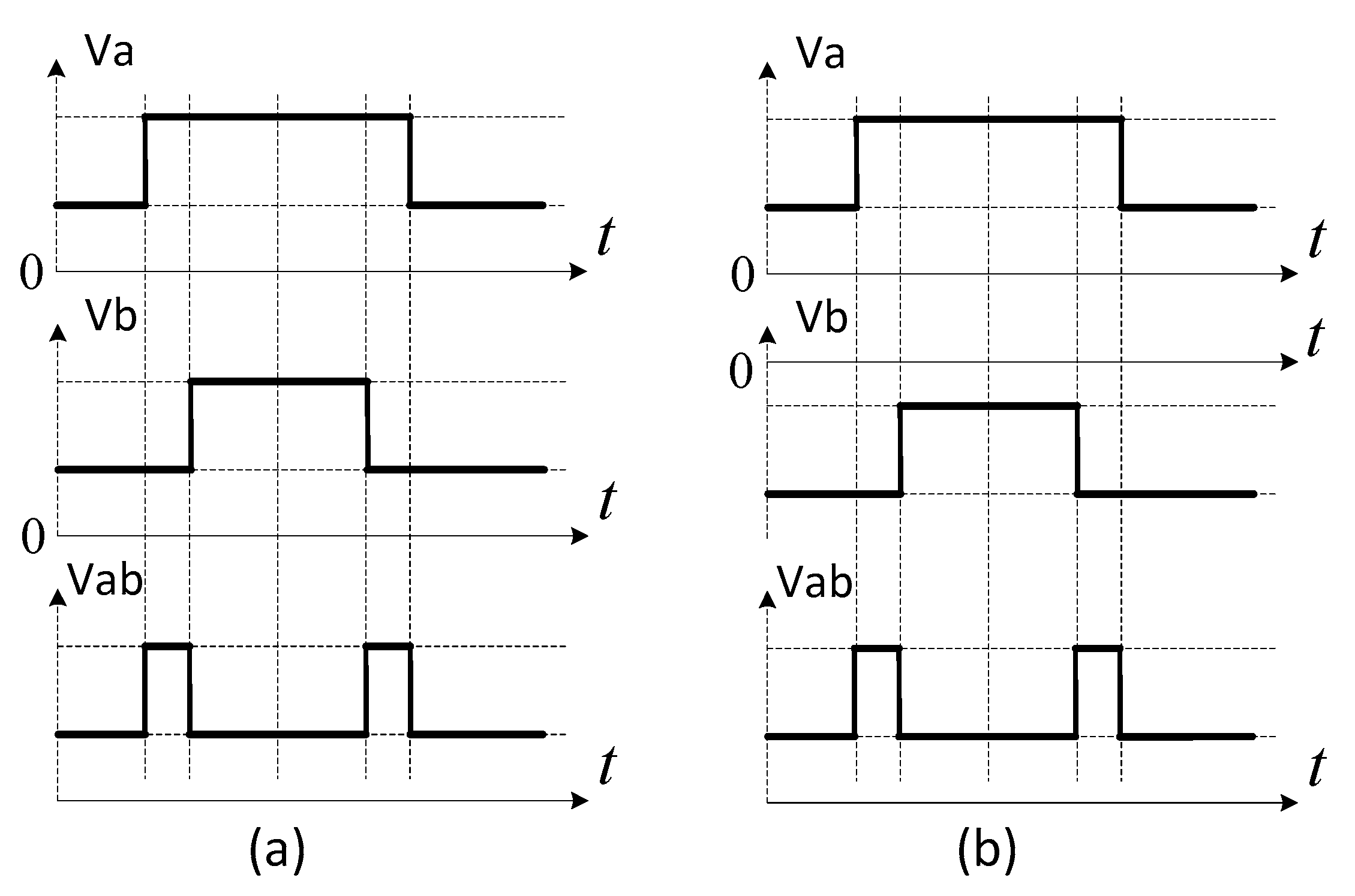
A single-phase CHB inverter topology and related phase-shifted (PS) and level-shifted (LS) PWM are demonstrated in
Figure 1. For LS PWM, apparent switching frequency equals the carrier one. For PS PWM, the apparent switching frequency is that of an individual H-bridge (double carrier frequency) times the number of H-bridges [
9].
Current THD theoretical calculations for a single-phase multilevel PWM inverter with uniform voltage level distribution and inductance-dominated RL-load is addressed in [
8]. The approach of [
8] is applicable to a CHB inverter with equal DC sources.
With respect to a CHB inverter having equal DC sources, a CHB inverter with non-equal DC voltages can affect current quality by introducing undesirable subharmonic content that may violate the grid-codes [
10].
This paper considers LS and PS PWM applied to single- and three-phase CHB inverters with non-equal DC sources in the context of current THD minimization. Though a converter RL-load is considered, the results are applicable to grid-connected applications as well [
8].
The paper starts with a generalization of asymptotic current THD formulas for a single-phase multilevel inverter with uniform levels [
8] for non-uniform voltage level distribution. The results are applicable to a single-phase CHB inverter with LS PWM and non-equal DC sources. In addition, minimal current THD requires matching LS PWM bands to DC source voltages that may be difficult to implement in real-life applications. For a single-phase CHB inverter with PS PWM and non-equal DC sources, the optimal current THD for more than three sources is achieved by a proper selection of carrier order (DC sources switching sequence), as recently shown in [
11,
12].
For a three-phase CHB inverter, theoretical current THD consideration becomes too complicated. Therefore, current THD is analyzed by MATLAB–Simulink simulations.
The major contributions of this paper may be formulated as follows. Theoretical current THD calculation methodology for non-uniform voltage levels allows evaluating current THD for a single-phase CHB inverter with non-equal DC sources and LS PWM. Though it is difficult to implement LS PWM in practice (PWM band matching to DC source voltages is required), the calculated current THD gives a theoretical limit.
For a three-phase CHB inverter with more than three DC sources per phase, the single-phase current THD optimal DC source switching sequences reported in [
11,
12] also work well. Swapping the carriers among the different phases (changing the carriers order) could be considered as an additional degree of freedom that may be used to improve the current THD.
The paper is organized as follows.
Section 2 presents the current THD calculation methodology for non-uniform voltage levels applicable to a single-phase cascade inverter in the case of LS PWM and non-equal DC sources. The analysis of the current THD with PS PWM and non-equal DC sources for the cascade H-bridge inverter is presented in
Section 3. The analysis of current THD has been extended to a three-phase cascade H-bridge inverter with non-equal DC sources and presented in
Section 4.
Section 5 presents the conclusion.
2. Current THD for a Single-Phase CHB Inverter with LS PWM and Non-Equal DC Sources
Current THD for a single-phase CHB inverter with LS PWM and equal DC sources can be calculated as suggested in [
8] for uniformly distributed voltage levels. In this section, the results of [
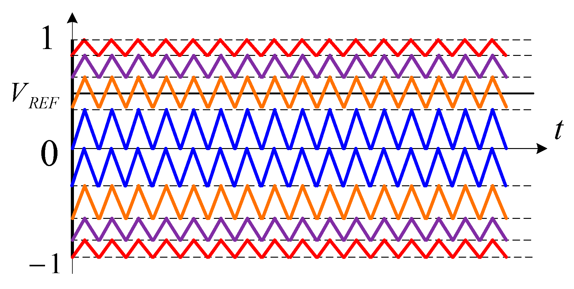
8] are generalized to acquire non-equal DC sources. For the best harmonic performance (minimal current THD), LS modulation bands must be adjusted to match non-equal DC source voltages (
Figure 2).
Current THD for inductance-dominated RL-load is calculated, similar to [
8], as
where
L and
R are load inductance and resistance;
ff and
fAS – fundamental frequency and apparent switching frequency;
n-level count (the number of H-bridges increased by one).
For
n-level CHB inverter with (
n − 1) H-bridges with non-equal sources and LS PWM band matching (
Figure 2), the current ripple normalized mean square (NMS) is found using the general formula
where
ai, 0 <
ai < 1, is “voltage level”,
i, 0 ≤
i ≤
n − 1, is the ratio of respective sum of DC source voltages to the total DC voltage (
a0 = 0,
an−1 = 1)
where
is the total DC voltage and
m is the modulation index (0 <
m < 1);
The current ripple NMS formula for two H-bridges (3-level)
For a three H-bridge (4-level) CHB with non-equal DC source voltages, V1 ≠ V2 ≠ V3, output voltage levels become .
Current ripple NMS for non-equal sources
where coefficients
are calculated using Formulas (6)–(8). For example, for a four H-bridge (5-level) CHB inverter current ripple NMS for non-equal sources from (2),
Theoretical current THD results obtained using (1), (2) are in good agreement with simulated ones. Calculations and simulations across this paper are carried out for the following parameters: load resistance R = 1 Ω, load inductance L = 1 mH, fundamental frequency ff = 50 Hz, apparent switching frequency fAS = 4000 Hz and nominal DC source voltage V = 100 V.
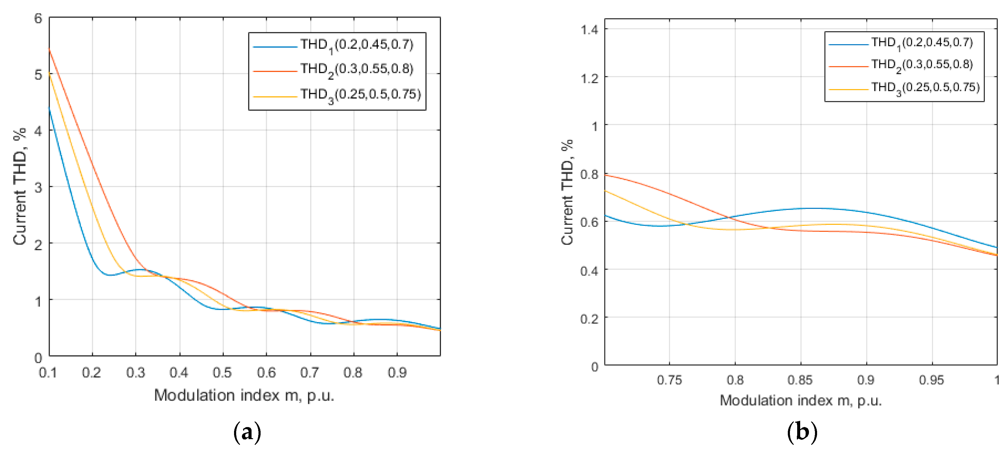
Figure 3a,b present theoretical current THD according to (1), (2), (11) for a single-phase 4-bridge CHB for three cases: non-equal sources arranged in ascending order (
); non-equal sources arranged in descending order (
); uniform voltage levels (equal sources,
).
For relatively large modulation indices m > 0.8, that is typical for grid-tied applications, current THDs for all three cases are close to each other. The lowest THD is achieved for non-equal sources arranged in descending order (V1 > V2 > V3 > V4).
For relatively small modulation indices m < 0.3, the lowest THD is achieved for the non-equal sources arranged in ascending order (V1 < V2 < V3 < V4).
Figure 4,
Figure 5 and
Figure 6 show current THD simulation results for
m = 0.9 that are in good agreement with theoretical ones (
Figure 3). Theoretical current THD values are typically slightly lower than those obtained from simulation due to theoretical assumptions.
The LS PWM considered in this section provides better current THD compared with PS PWM for single-phase and especially for three-phase CHB inverters. However, the known drawback of LS PWM is an uneven power and loss distribution across different H-bridges. For equal DC sources, the remedy may be H-bridge rotation. For non-equal DC sources, the best THD performance requires LS PWM band adjustment in accordance with true DC source voltage magnitudes (
Figure 2) that may become problematic. If there is no match between non-equal DC sources and LS PWM bands, current THD is compromised, and the linearity of CHB inverter as reference signal “voltage amplifier” is violated.
3. Current THD for a Single-Phase CHB Inverter with PS PWM and Non-Equal DC Sources
For a single-phase CHB inverter with PS PWM and equal DC sources (uniform levels), current THD for inductance-dominated RL-load may be calculated according to [
8]. Current THD theoretical formulas are based on asymptotic assumption, meaning that the apparent PWM frequency is much larger than the fundamental AC one.
In theory, the same formula for current THD for uniform voltage levels is applicable to both LS and PS PWM. In real life, current THD for PS PWM may be larger than that for LS PWM, that is better predicted by asymptotic formulas.
For LS PWM, voltage and current spectra show distinct apparent switching frequency (
Figure 4,
Figure 5 and
Figure 6). For PS PWM, the spectrum around apparent switching frequency is spread. This happens because, at reference level crossings, PWM voltage for PS PWM is shifted by half a PWM period. This effect has almost no impact on voltage THD for uniform levels—for a single-phase CHB inverter with equal sources, voltage THD is practically the same for both LS and PS PWM, and this is because voltage ripple mean square on respective PWM periods is practically the same [
7].
The effect of PWM voltage half a period shift at reference level crossings, in fact, presents a low-frequency disturbance that may have a negative impact on current THD. This is because current ripple can be considered as voltage ripple integral for an inductance-dominated load [
8], and it is deteriorated by the low-frequency “voltage irregularities”. On the one hand, this adverse effect increases with level count increase (more reference voltage crossings). On the other hand, it reduces with apparent switching frequency increase (more switching between adjacent levels) and RL-load time constant increase (better low-frequency filtering).
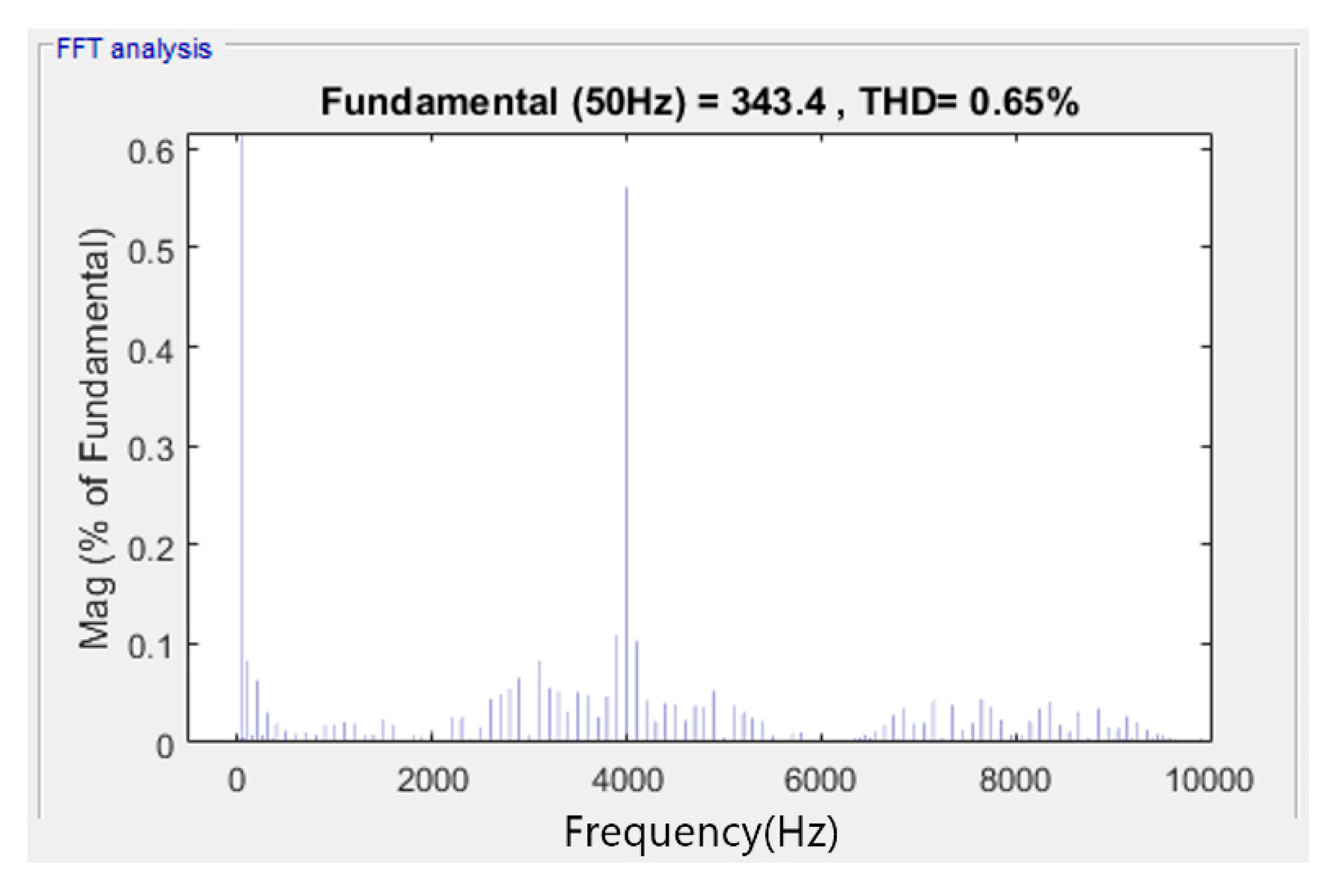
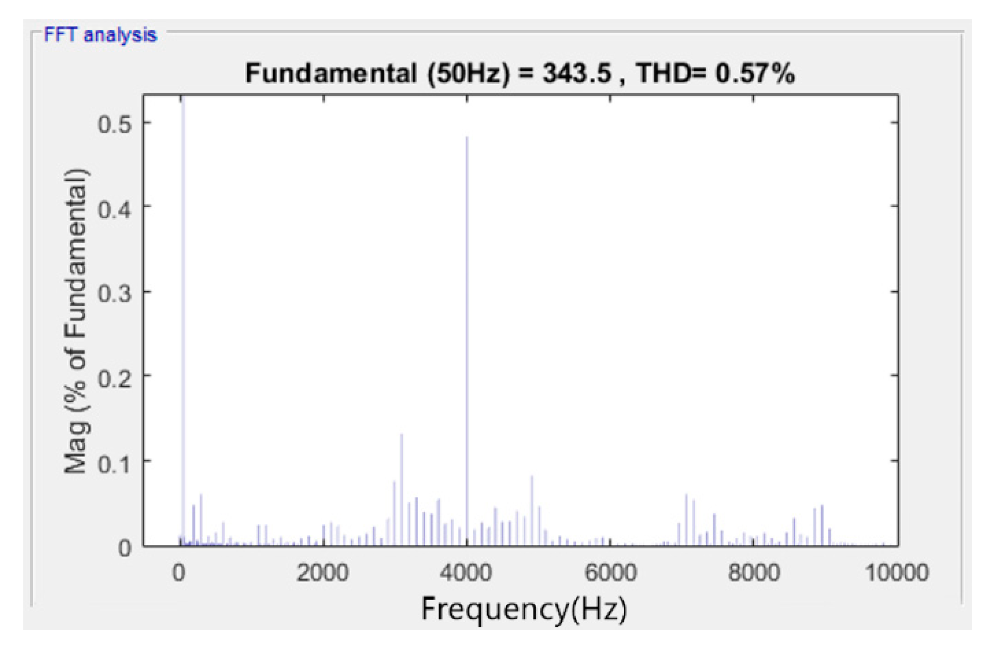
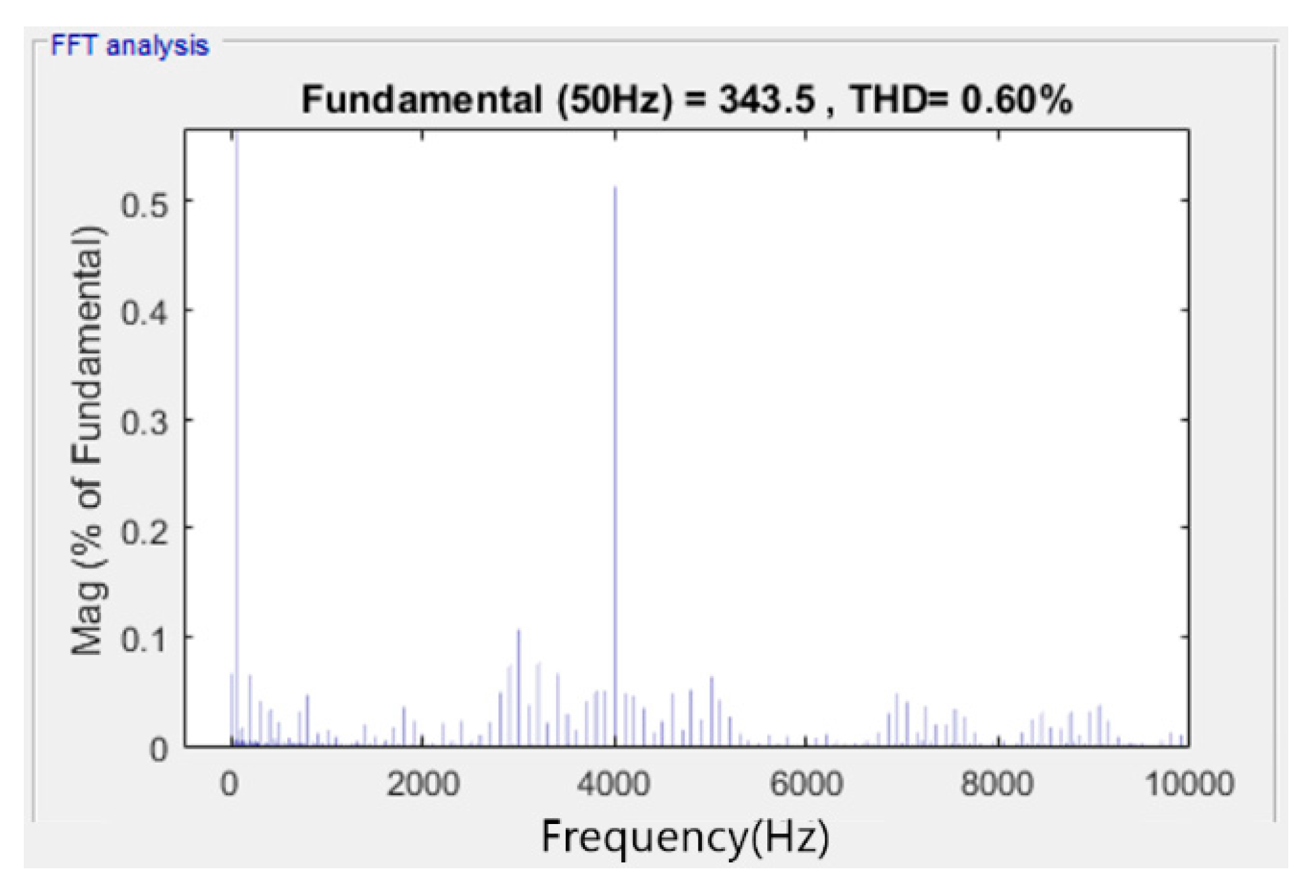
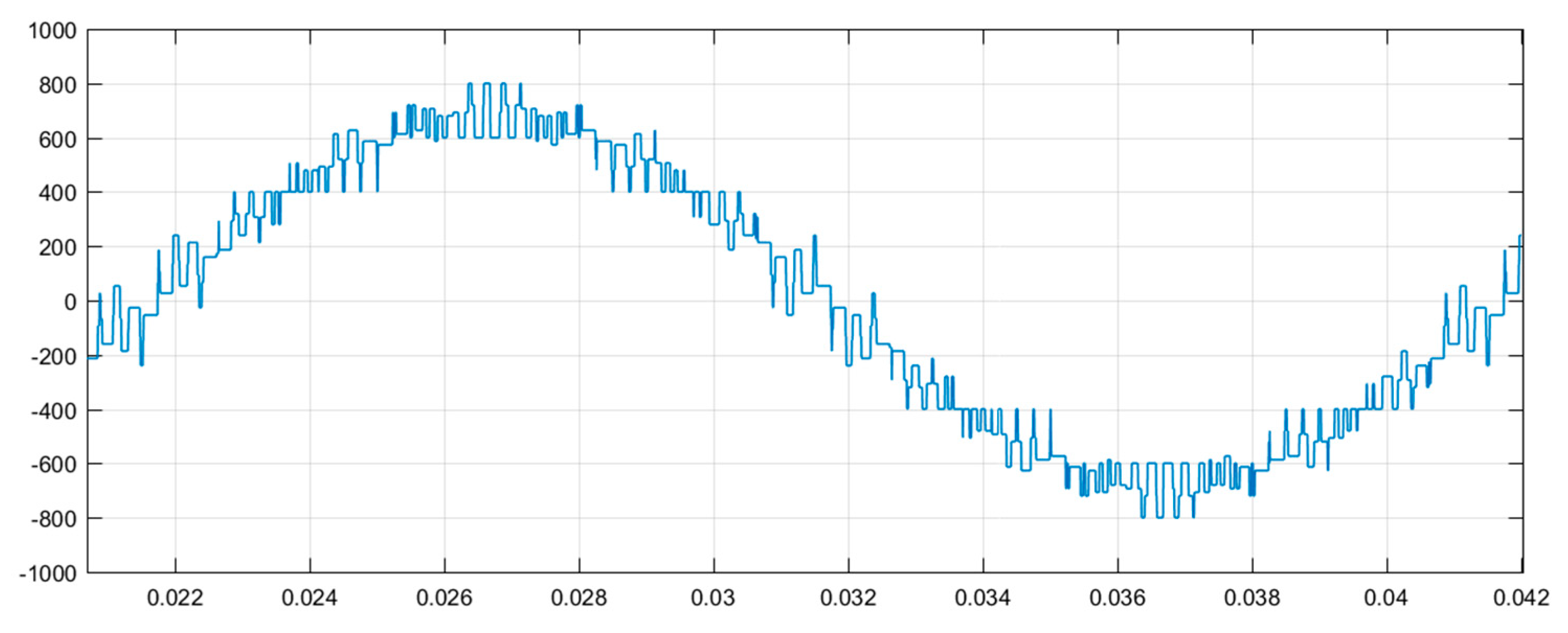
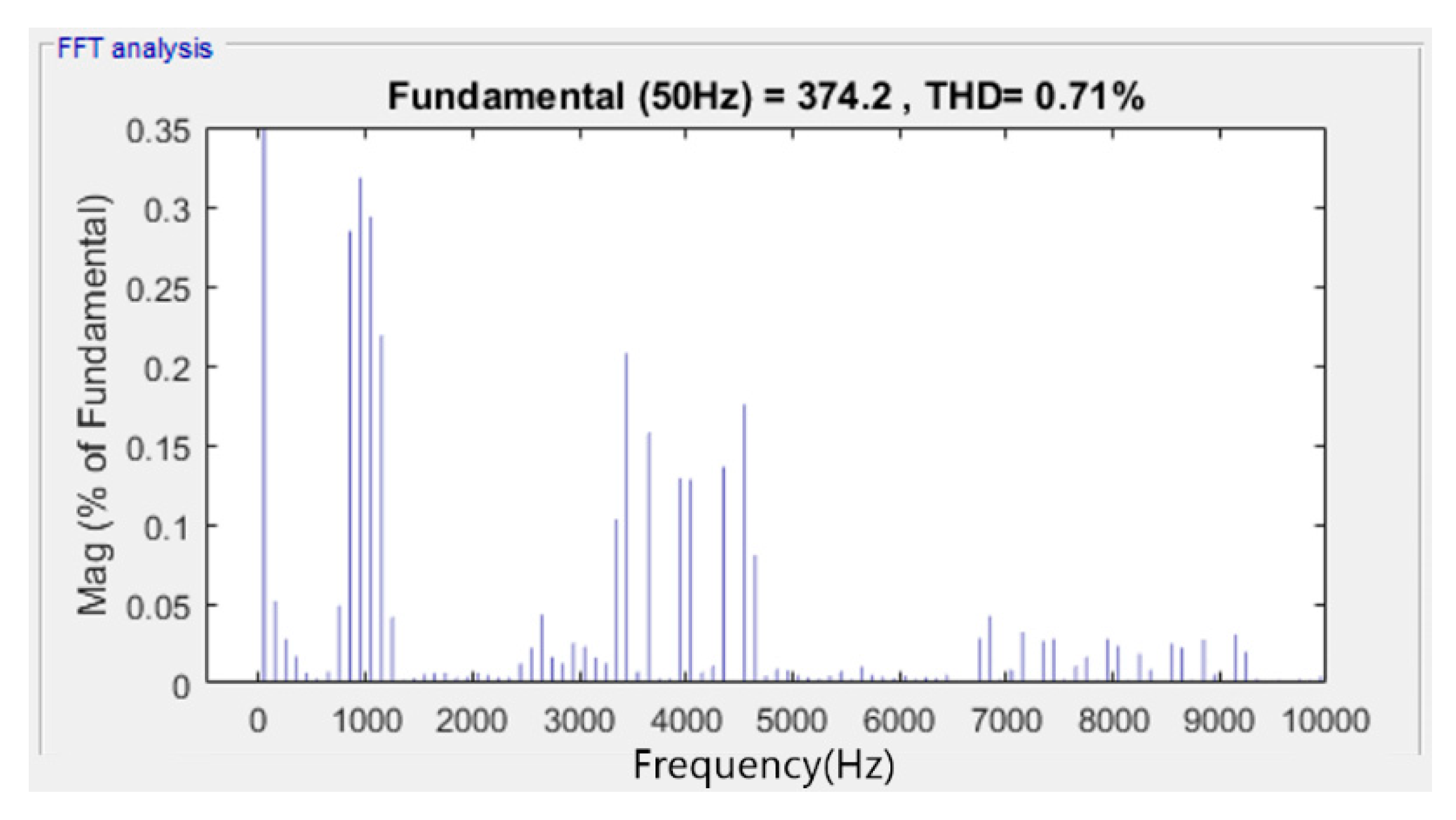
Figure 7 shows current THD for a four H-bridge CHB inverter with equal sources and PS PWM. Compared with LS PWM for the same modulation index
m = 0.9 (
Figure 6), the switching frequency spectrum is spread, and the THD value is slightly larger.
In the recent papers [
11] and [
12], asymptotic formulas of [
8] are generalized for a single-phase CHB inverter with PS PWM and non-equal DC sources. Moreover, it is shown that for more than three H-bridges, there are extreme DC source (H-bridge) switching sequences (carrier orders in
Figure 1b that minimize (maximize) current THD.
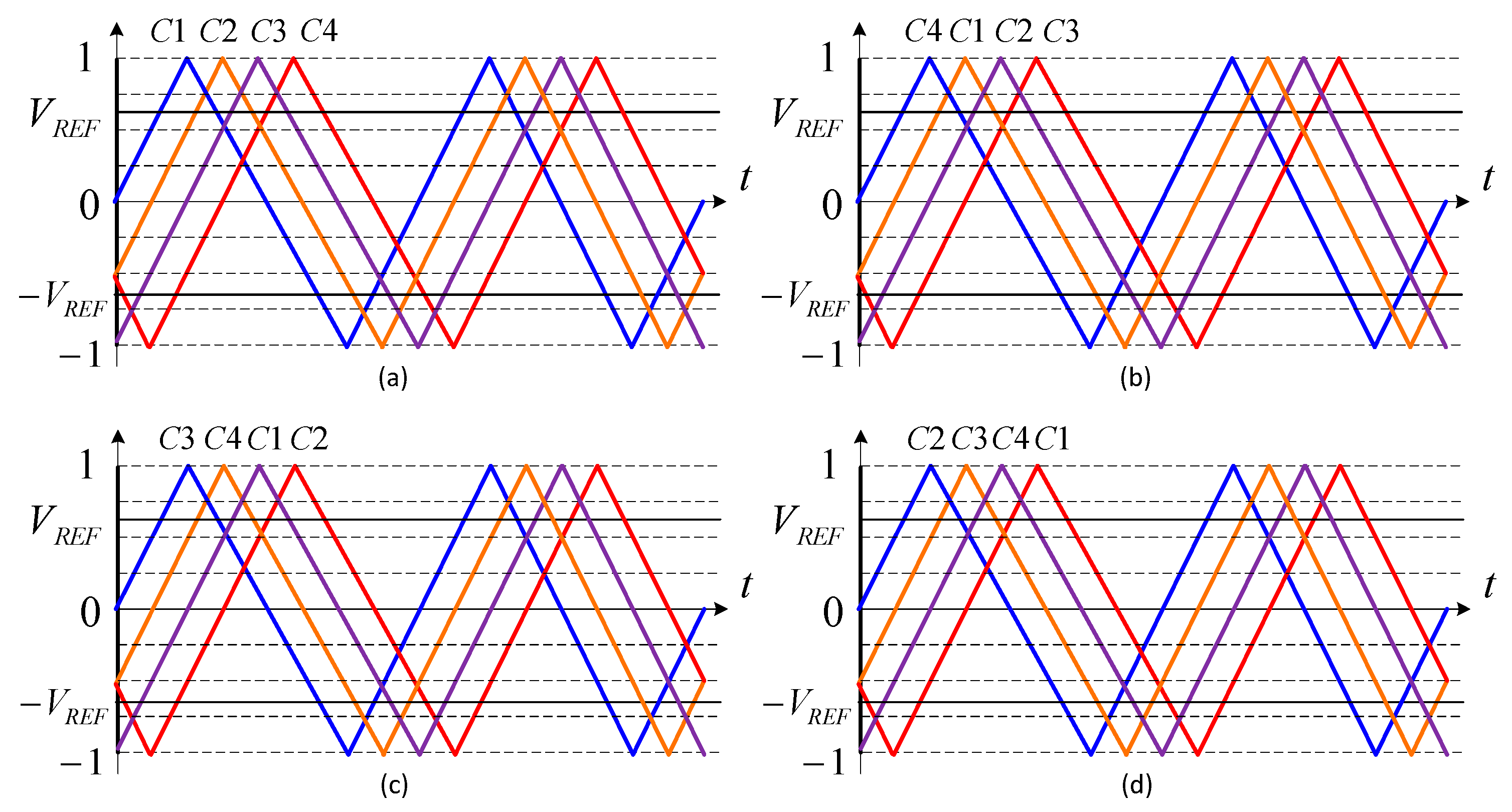
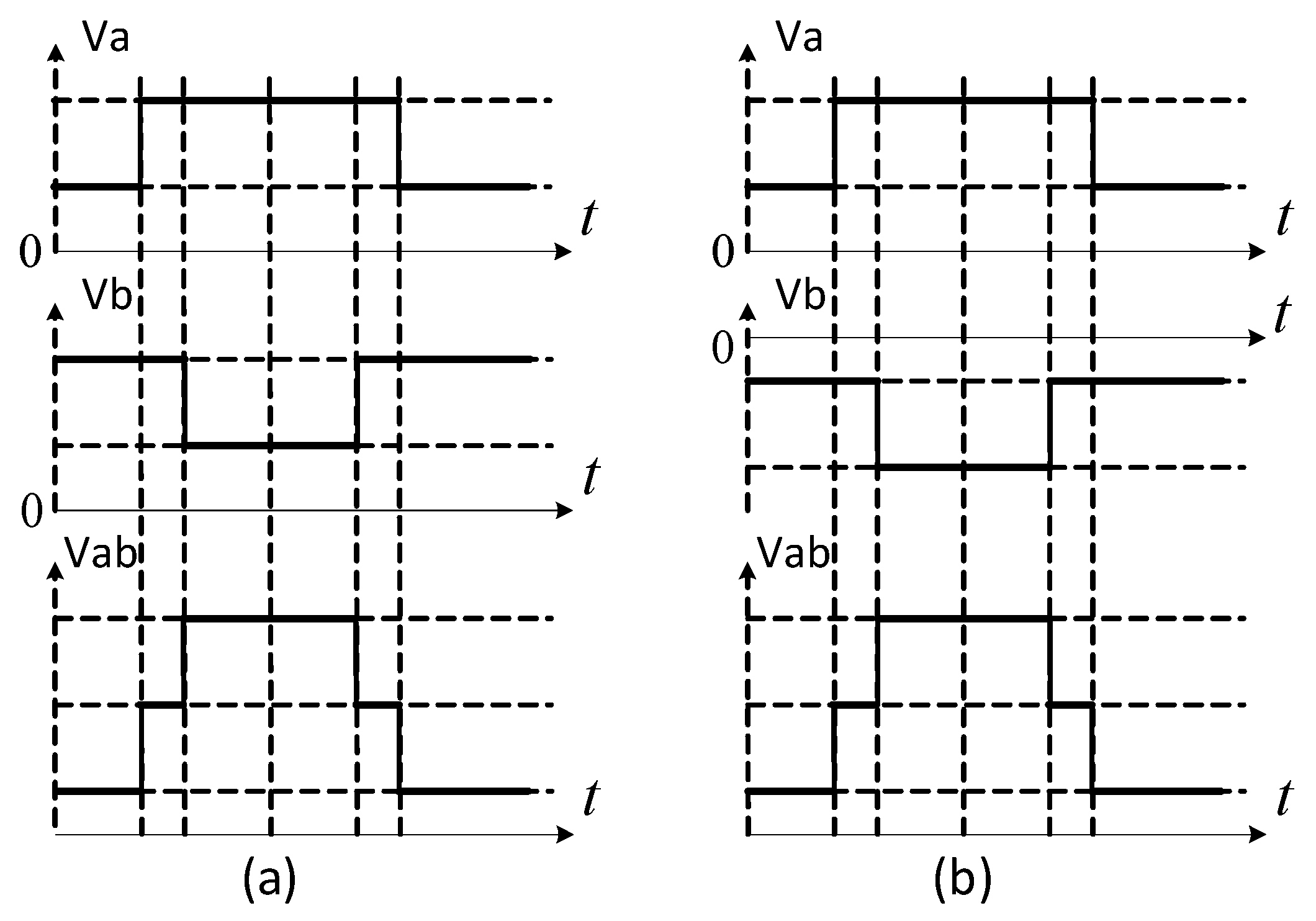
Suppose DC source voltages are sorted in the ascending order
and DC source switching sequences on a PWM period are denoted by number sequences like 1234 (
Figure 8). In the case of three CHB cells, there are six different sequences in total, and only one sequence could be considered with respect to the THD, which is the 123. In fact, the sequences 123, 231, and 312 have the same THD due to circular permutation equivalence. Similarly, 321, 132, and 213 have the same THD due to the reversal circular permutation. In the following, “1” is always placed first to eliminate circular permutation redundancy.
In the case of four CHB cells, only three different sequences can be considered which are 1234, 1324, and 1243. The other sequences are equivalent within circular permutation (
Figure 8) and order reversal. The number of all possible DC source switching sequences for the different numbers of H-bridge cells are summarized in
Table 1. It can be noticed that in the case of four and more CHB cells, the THD with PS PWM is strictly dependent on the DC sources switching sequences.
As shown in [
11,
12], for four H-bridges, the best and worst sequences from the current THD perspective become 1423 and 1243. The switching sequences for the different numbers of H-bridge cells are given in
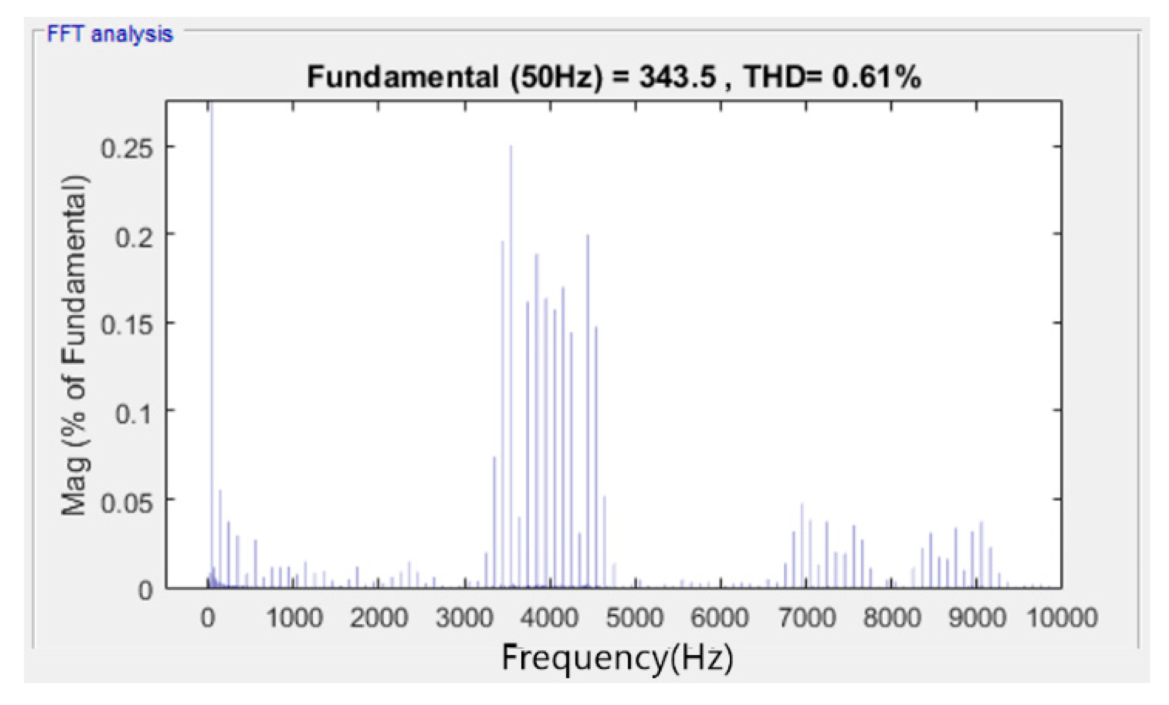
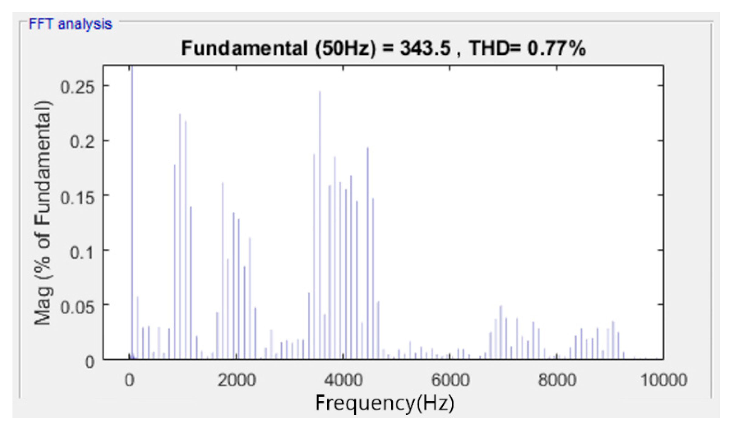
Table 2 with respect to the best and the worst cases.
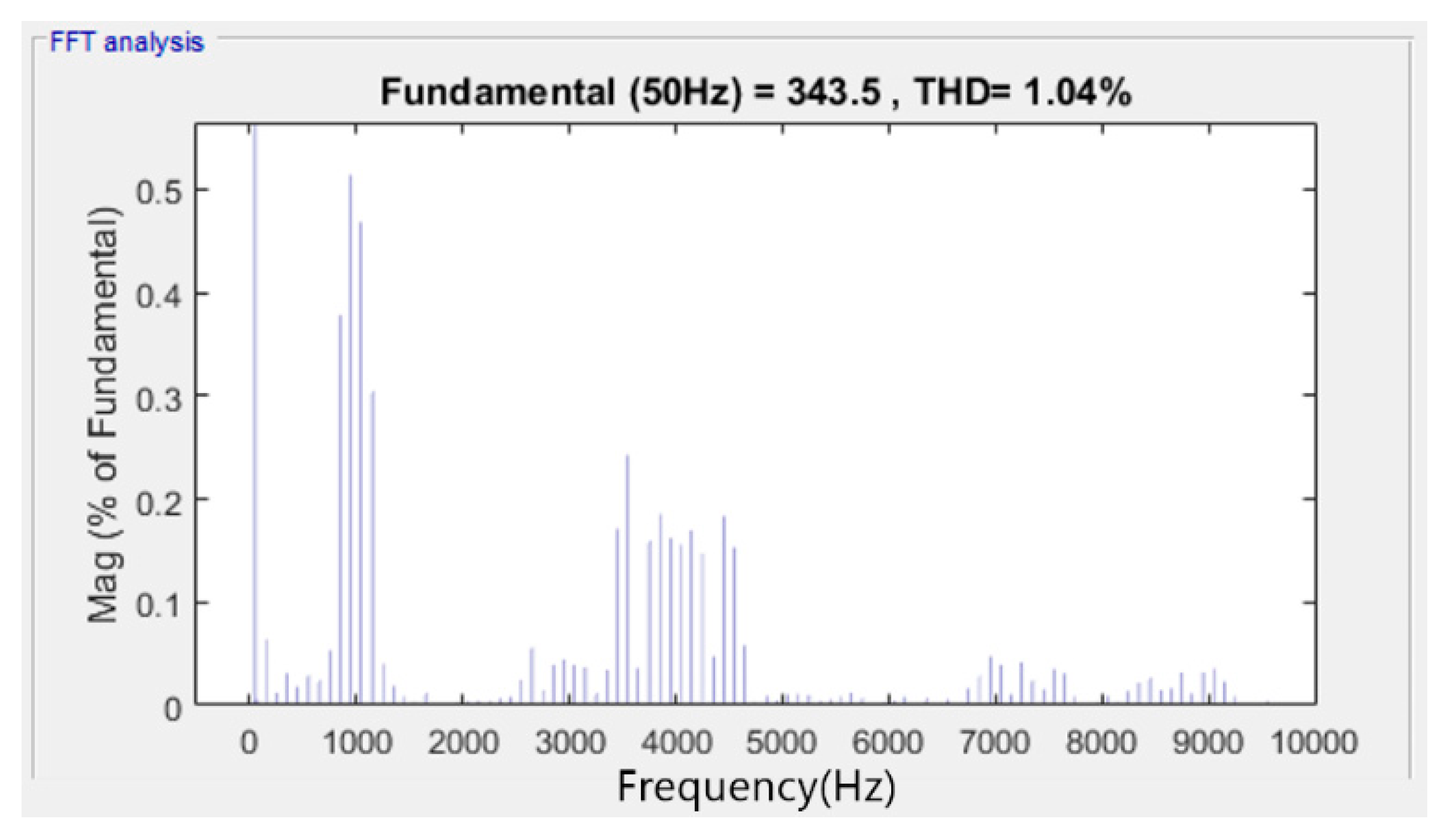
Figure 9 and
Figure 10 present current THD for a single-phase CHB inverter with PS PWM for the best and worst switching sequences, respectively. Normalized non-equal voltages amount to
v1 = 0.8;
v2 = 0.933;
v3 = 1.067;
v4 = 1.2 p.u. (1.0 p.u. corresponds to 100 V). It is clearly seen that the best source switching sequence, 1423, provides the minimal current THD of 0.77% (1.04% for the worst sequence). However, the minimal THD of this PS PWM is worse than 0.6% for equal DC sources (for LS PWM with optimal bands adjustment, it is even better—0.57%).
Current THD was also calculated for a single-phase CHB inverter with six H-bridges and PS PWM for the best and worst switching sequences, respectively. Normalized non-equal voltages were selected as v1 = 0.80; v2 = 0.88; v3 = 0.96; v4 = 1.04; v5 = 1.12; v6 = 1.20 p.u. Current THD for the best switching sequence 162435 was found as 0.47%, and the same for the worst sequence—1.29% (compared with 0.4% for equal DC sources).
Current THD values for different cases of single-phase four H-Bridge CHB inverter PWM for
m = 0.9,
R = 1 Ω,
L = 1 mH are compared in
Table 3.
In general, there was a good agreement between theoretically calculated and simulated values. For uniform levels, simulated current THD for PS PWM was slightly larger than for LS PWM due to the unaccounted effect of PS PWM voltage half a period shift at reference level crossings (
Section 2).
Current THD values for different cases of single-phase six H-Bridge CHB inverter PWM for
m = 0.9,
R = 1 Ω,
L = 1 mH are compared in
Table 4.
For
Table 4, again, there is a good agreement between theoretically calculated and simulated current THD values. The relative difference between calculated and simulated current THD values for PS PWM is larger compared to the four H-bridge inverter because there are more unaccounted low-frequency disturbances due to PWM voltage half a period shift at reference level crossings.
4. Current THD for a Three-Phase CHB Inverter with Non-Equal DC Sources
Voltage and current quality for three-phase CHB inverters with equal DC sources for LS PWM are reported in the literature to be better than for PS PWM [
13,
14,
15]. The presented frequency domain explanations seem to be complicated as they involve double Fourier series spectra calculations, sideband frequencies, etc. Presented below is an elementary time domain explanation of LS PWM superiority for three-phase converters.
The indication of modulation strategy quality for a three-phase converter is line voltage quality. For both LS and PS PWM, generated source phase voltage is of optimal nearest level switching quality. However, while for LS PWM line (phase-to-phase) voltage is still of nearest level switching type, for PS PWM, it becomes non-nearest switching that deteriorates voltage and current quality.
An elementary time domain explanation of this phenomenon is based on the effect of PS PWM voltage half a period shift at reference level crossings, as discussed in
Section 2. It is about synchronization of source voltage waveforms of different phases because a line voltage is obtained as a difference between two phase voltages.
Figure 11 demonstrates the synchronization of PWM voltages of different phases for LS PWM (no matter what the specific voltage levels are).
Figure 11a shows that for the pulses of the same polarity, LS PWM provides middle pulses synchronization. For the pulses of opposite polarities (
Figure 11b), a middle of the pulse (peak) in one phase is synchronized with a middle of the pause (valley) in another phase. As line voltage
Vab is obtained by subtracting phase voltage
Vb from
Va, it is the optimal nearest level switching type. Also note the line voltage frequency doubling effect.
For PS PWM, due to the effect of voltage half a PWM period shift at reference level crossings, for some portions of a fundamental period different phase, PWM voltage synchronization may be as in
Figure 12 (
Figure 12b is obtained from
Figure 11b by half a PWM period shift). This kind of synchronization results in reduced line voltage quality due to non-nearest level switching.
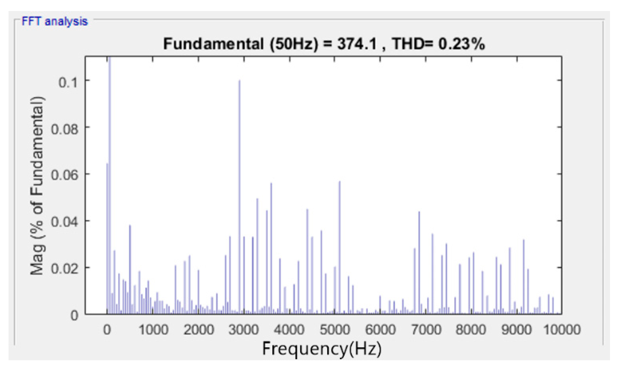
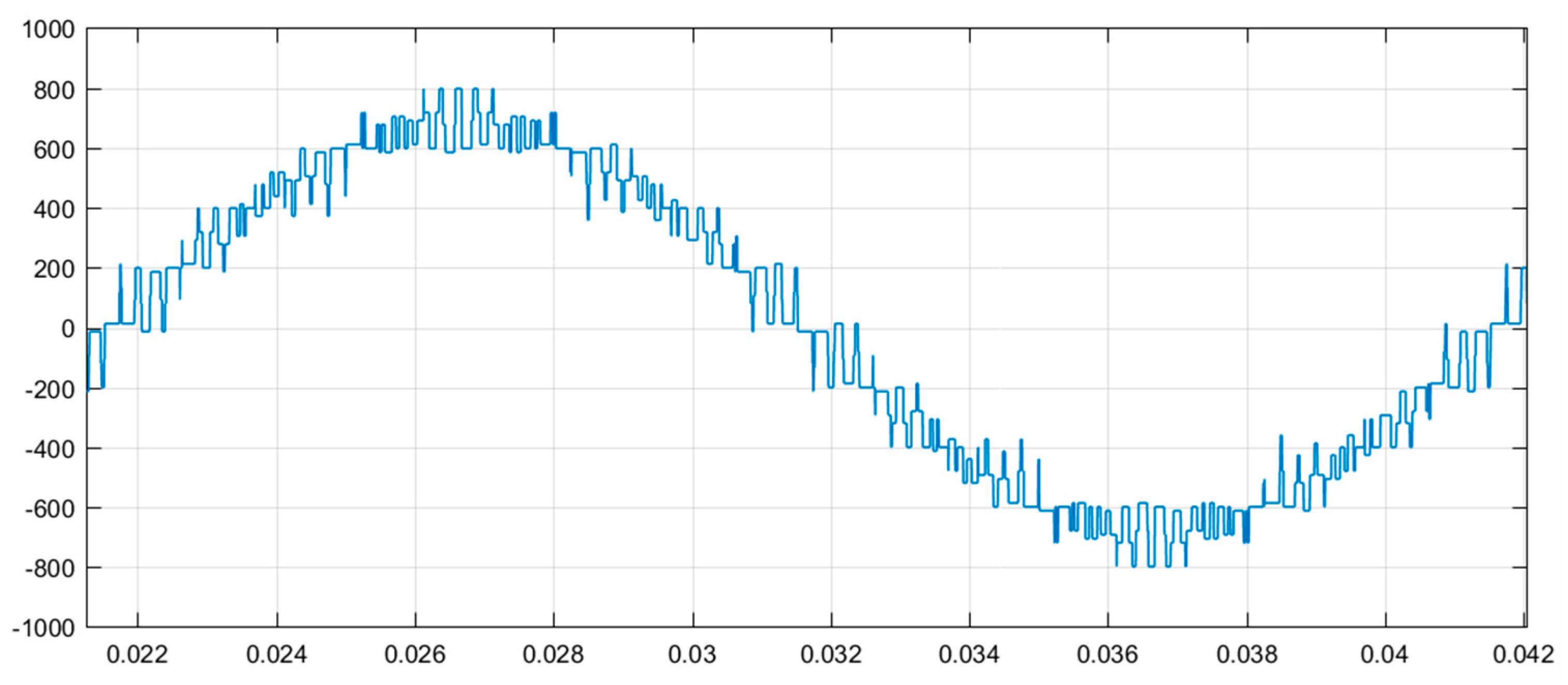
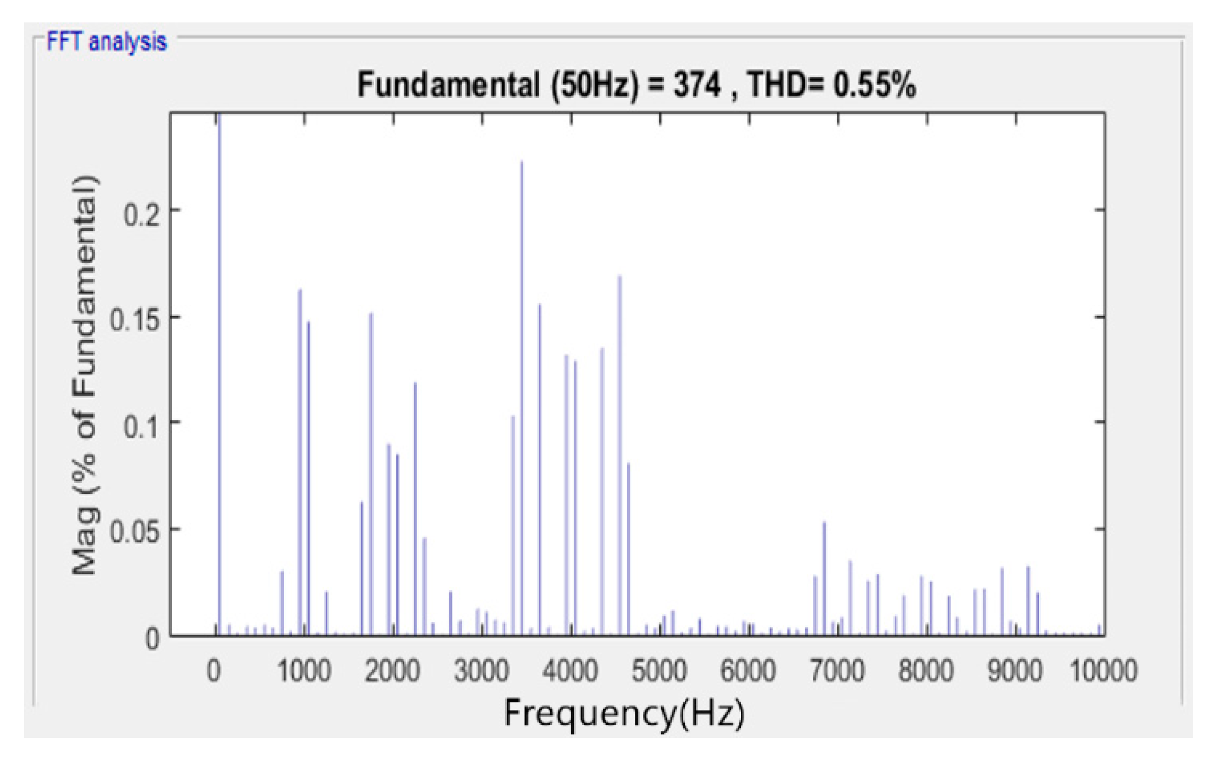
Theoretical asymptotic time domain analysis of a three-phase CHB inverter voltage and current quality becomes a complicated task. Therefore, current THD values in this section were obtained by simulation for inverter Y-connected balanced RL-load and relatively large modulation index m = 0.85 that is characteristic for grid-tied applications. Voltage references were selected pure sinusoidal without any zero-sequence insertion.
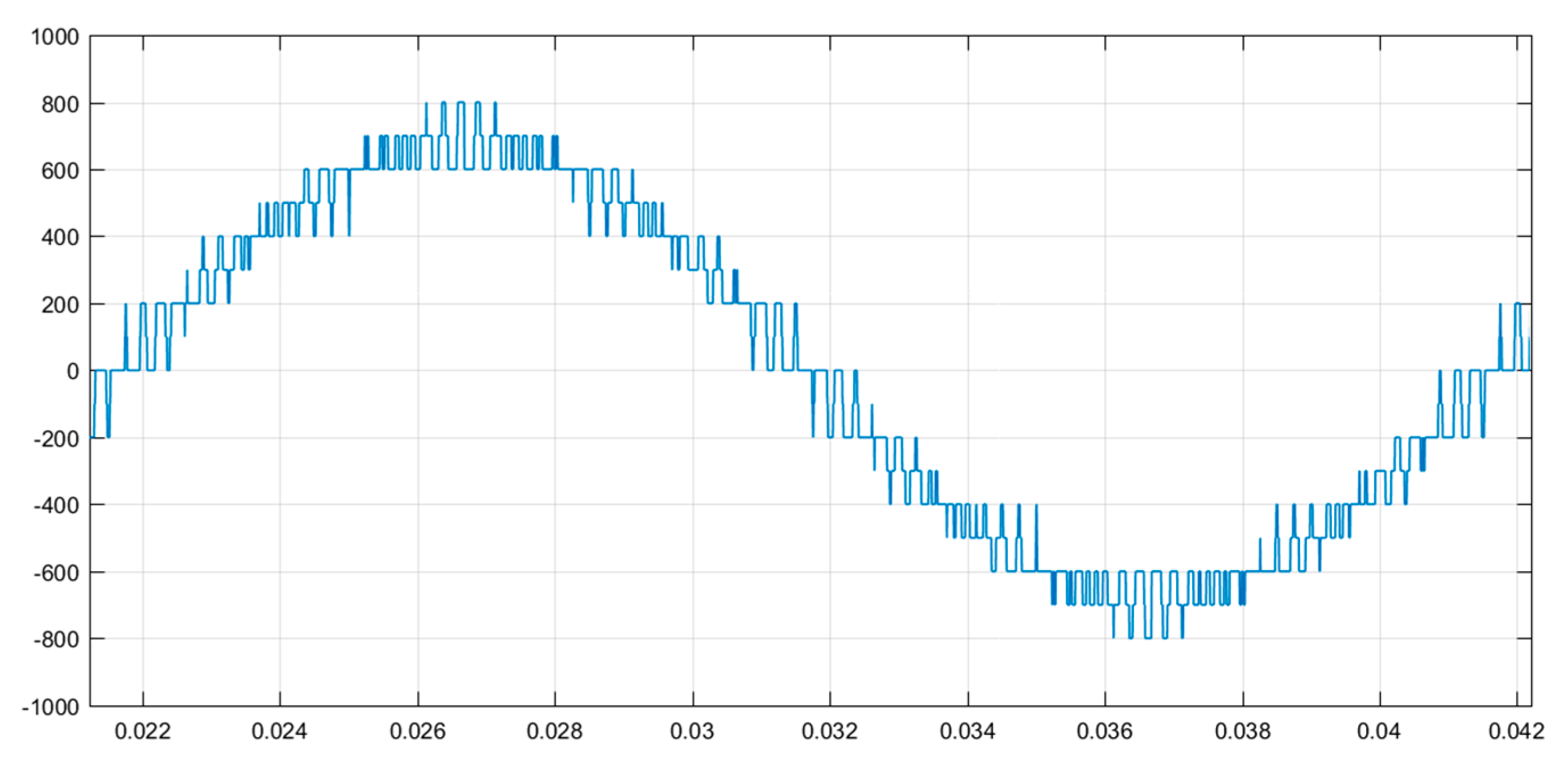
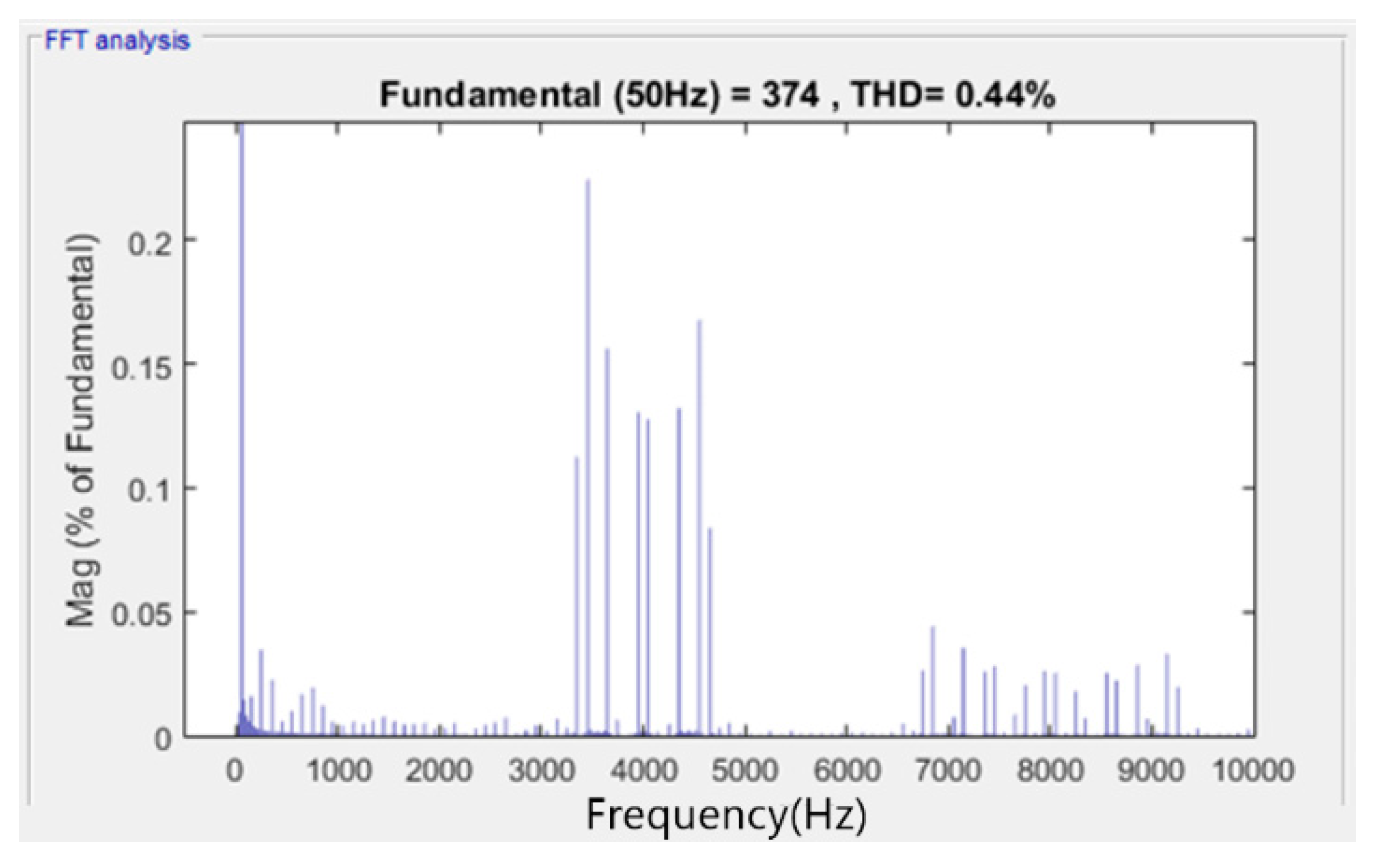
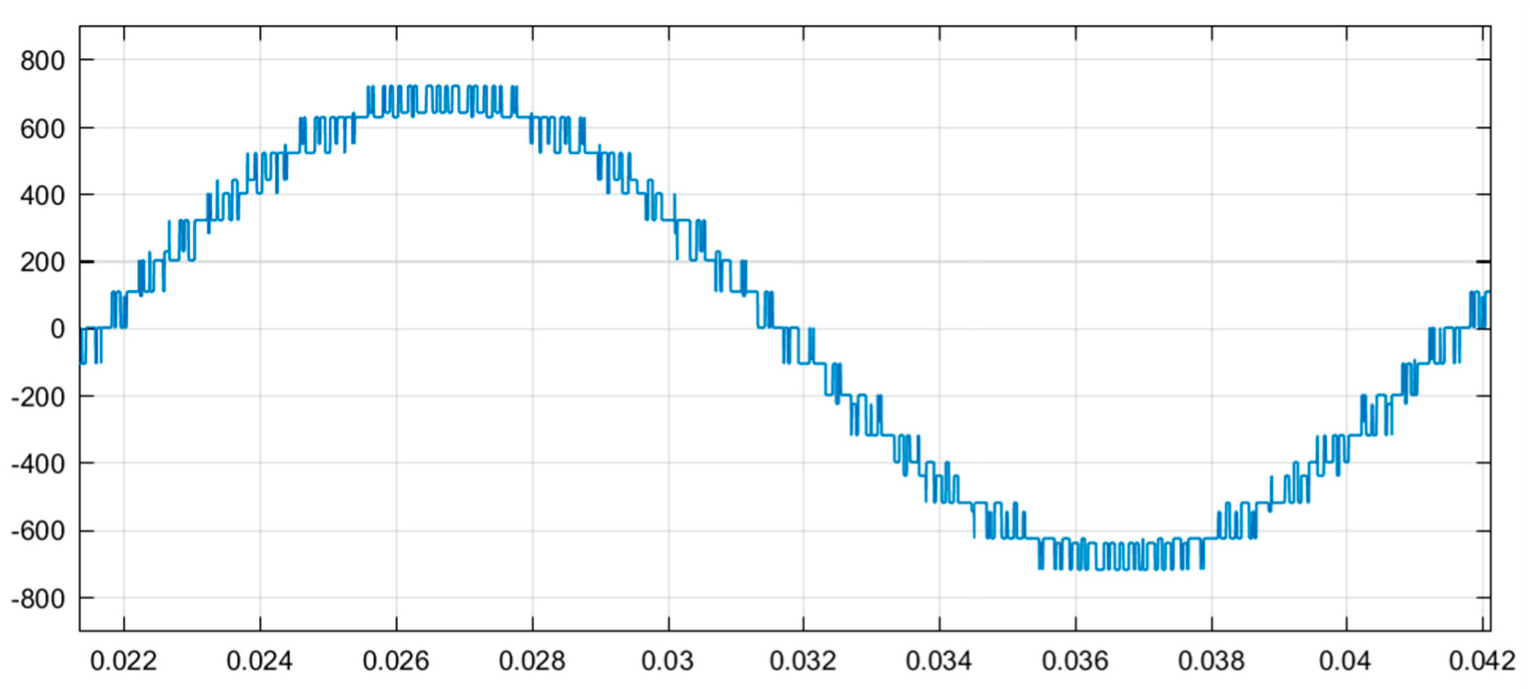
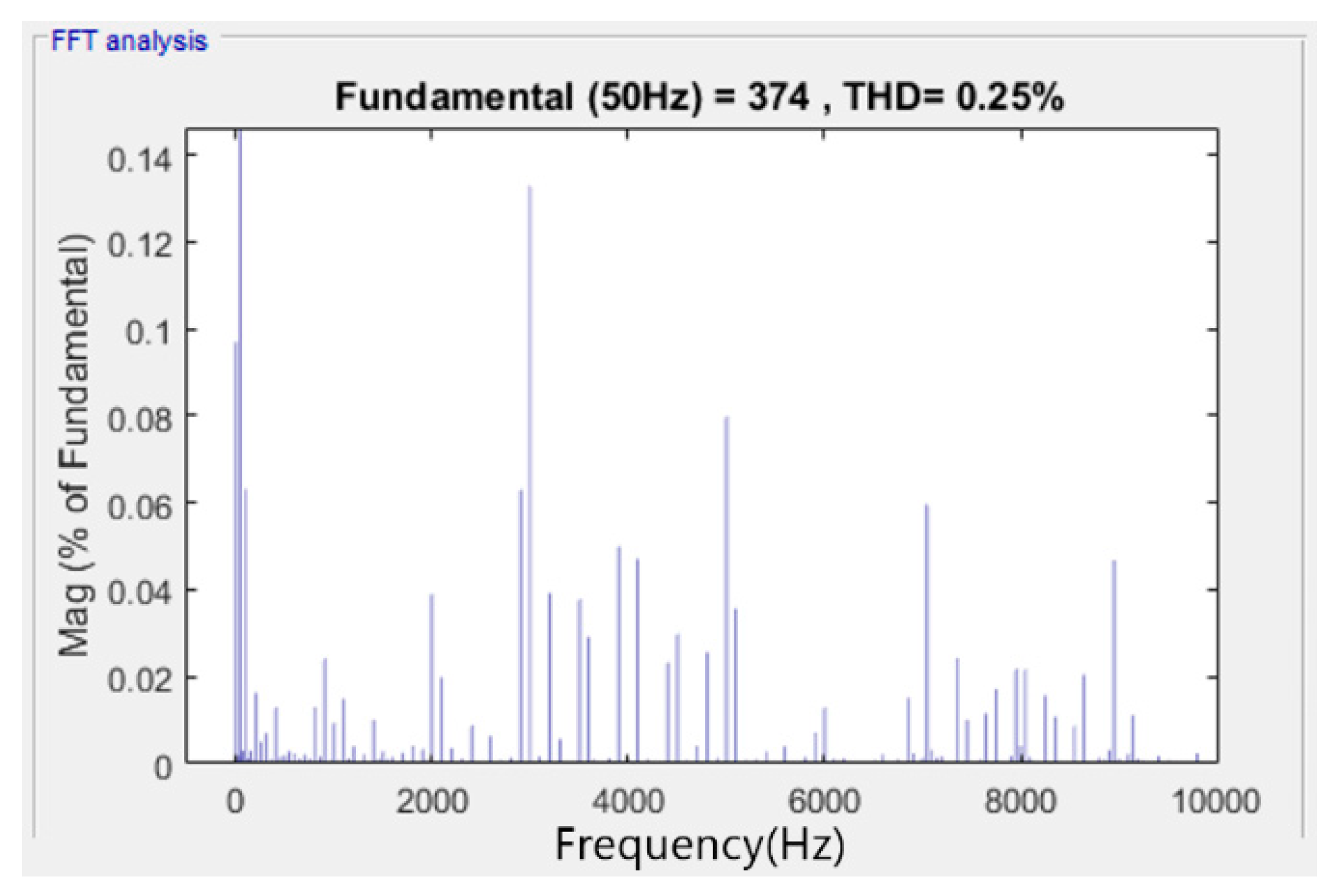
For LS PWM and equal DC sources, line voltage and current THD are shown in
Figure 13 and
Figure 14; the same for PS PWM—in
Figure 15 and
Figure 16. It is clearly seen that for PS PWM, for some parts of the fundamental period, the line voltage is of the non-nearest switching type that results in current THD increase from 0.23% (in case of LS PWM) to 0.44%.
Next, consider non-equal DC sources. In this paper, for the sake of simplicity, we assume the same non-equal sources in all three phases. Specifically, for a four H-bridge CHB inverter, normalized voltages v1 = 0.8; v2 = 0.933; v3 = 1.067; v4 = 1.2 p.u. (1.0 p.u. corresponds to 100 V).
For the four H-bridge CHB inverter with LS PWM and phase DC sources arranged in the optimal descending order, line voltage and current THD are given in
Figure 17 and
Figure 18. Again, this excellent current quality is achieved for ideal matching of LS PWM bands to DC sources that may be difficult to implement in practice.
For PS PWM, there is another degree of freedom which is carriers’ synchronization in different phases. The results of
Figure 19,
Figure 20,
Figure 21 and
Figure 22 were obtained assuming the same carriers for all three phases. For example, for the best sequence, the carrier sequences in three phases are (1423; 1423; 1423). However, the carriers in different phases can be shifted using circular permutation without violating phase switching sequence optimality, e.g., (1423; 3142; 2314).
If the number of sources in CHB inverter phase is not a multiple of 3, then such carriers’ manipulation will always make voltages and currents non-symmetric, and current THDs in different phases will be unequal. The authors have an example showing that current THD in each phase may become less than the one obtained when using the same carrier sequence in three phases.


