Article

A Single-Phase Nine-Level Boost Inverter

1
Faculty of Electrical and Electronics Engineering, Ho Chi Minh City University of Technology and Education, 1 Vo Van Ngan Street, Thu Duc district, Ho Chi Minh City 700000, Vietnam
2
Department of Electrical Engineering, Chosun University, 309 Pilmun-daero, Dong-gu, Gwangju 61452, Korea
*
Author to whom correspondence should be addressed.
Energies 2019, 12(3), 394; https://doi.org/10.3390/en12030394
Submission received: 31 December 2018 / Revised: 21 January 2019 / Accepted: 25 January 2019 / Published: 27 January 2019
(This article belongs to the Section F: Electrical Engineering)

Abstract

:
A novel single-phase nine-level boost inverter is proposed in this paper. The proposed inverter has an output voltage which is higher than the input voltage by switching capacitors in series and in parallel. The maximum output voltage of the proposed inverter is determined by using the boost converter circuit, which has been integrated into the circuit. The proposed topology is able to invert the multilevel voltage with the high step-up output voltage, simple structure and fewer power switches. In this paper, the circuit configuration, the operating principle, and the output voltage expression have been derived. The proposed converter has been verified by simulation and experiment with the help of PSIM software and a laboratory prototype. The experimental results match the theoretical calculation and the simulation results.

1. Introduction

Recently, multilevel inverters (MIs) have played important roles for high-power applications because of their advantages as better output voltage waveforms quality, a reduced rating of power semiconductor devices, and low electromagnetic interference [1]. The traditional MI topologies are neutral-point-clamped (NPC), flying-capacitor (FC), and cascade H-Bridge (CHB) inverters [2,3,4,5]. Diodes and capacitors are used to generate multilevel at the output voltage in NPC and FC inverters, respectively. On the other hand, to attain voltage levels, the direct current (DC) source must be increased. Nevertheless, both the circuit configurations and their controls become very complicated along with the increasing number of the output voltage levels. Furthermore, these topologies also make capacitors’ imbalanced. Some in-depth studies for NPC’s topologies have been presented in References [6,7,8]. To operate at the higher voltage level, the CHB inverters are used thanks to easy modularization and facilitate to expansion extension [9,10]. However, the topologies request more and more power devices with separate DC voltage sources. When the output voltage has more levels, the number of the required input DC sources is increased. Construction of a multilevel converter was introduced in Reference [11] with the use of multiple modules that made it easy to expand. However, this also increases the number of capacitors and switches required.
A seven-level inverter using series-connected DC voltage sources was presented in Reference [12] with the use of multiple DC voltage sources supplies to reduce switching losses. However, the number of output voltage levels depends on the number of DC voltage sources. A circuit of (4n + 3)-level inverter using voltage sources in serial/parallel operation was introduced in Reference [13] to increase the number of output voltage levels with the complex pattern and increase the conductive losses. By using an additional boost converter to create a multi-step output with capacitors, a seven-level grid-connected inverter for photovoltaic systems was presented in Reference [14], but an imbalance between capacitors is very likely to occur.
Nowadays, the switched-capacitor (SC)-based MIs are a popular solution for single-phase systems because they have a simple topology and reduce the component count. In Reference [15], a serial/parallel connection-based MI was presented. The topology of a SCMI for high-frequency aternative current (AC) microgrids was proposed in Reference [16]. SCMIs are recommended in Reference [17] with the ability to balance capacitor voltage and step-up voltage. The formerly SCMI topologies consist of SC elements with a high-voltage DC source. Then, they are divided into several floating DC sources [15,16,17,18,19] or a cascaded combination of multiple SC converters [20,21,22,23]. However, in most of these topologies, the voltage across the capacitors is only equal to the supply voltage. Therefore, the output voltages are limited. To overcome this limitation, the topology of the single-phase step-up five-level inverter was introduced in Reference [24], which uses the switch-diode-capacitor (SDC) circuit [25] and an additional booster circuit to increase the input voltage. In summary, Table 1 shows the advantages and disadvantages of the multilevel inverters with reduced switch count.
In this paper, a new nine-level boost inverter (NLBI) is suggested. The NLBI is an extension of the five-level inverter in Reference [24]. The NLBI combines structure switched-diode-capacitor, switched-capacitor, a conventional boost converter, and an H-bridge circuit to be able to enhance boost ability of output voltage levels with the reduced circuit components. In Section 2, the topology, operating principles and circuit analysis of the proposed inverter are presented. Section 3 presents the selection of the inductor and the capacitor. Simulation and experimental results are shown in Section 4. Finally, the conclusion is summarized in Section 5.

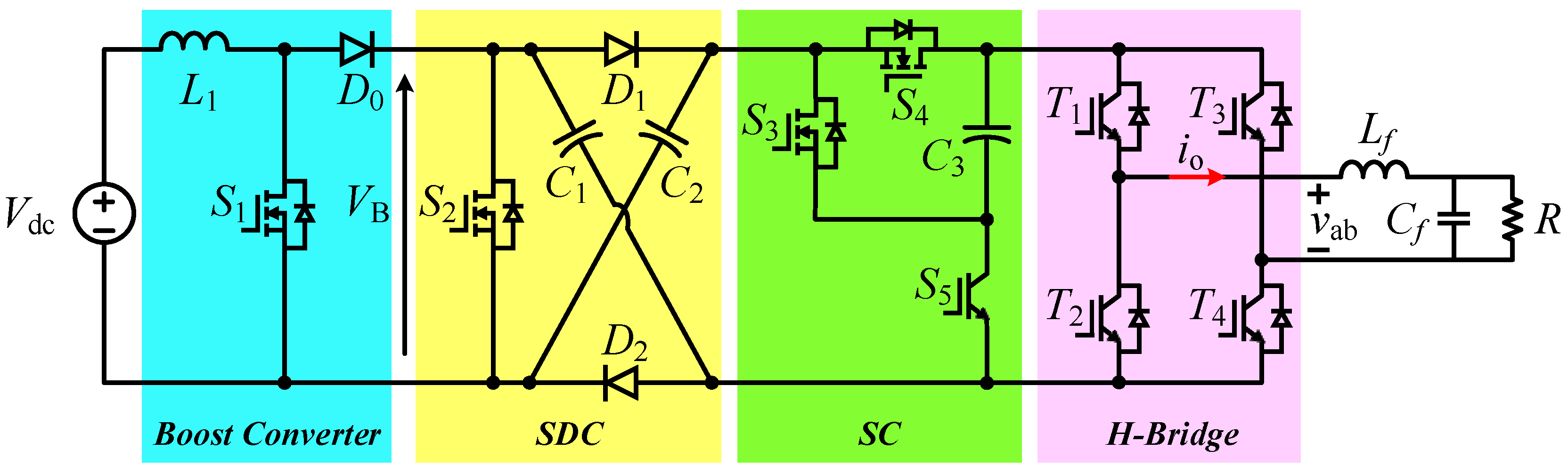
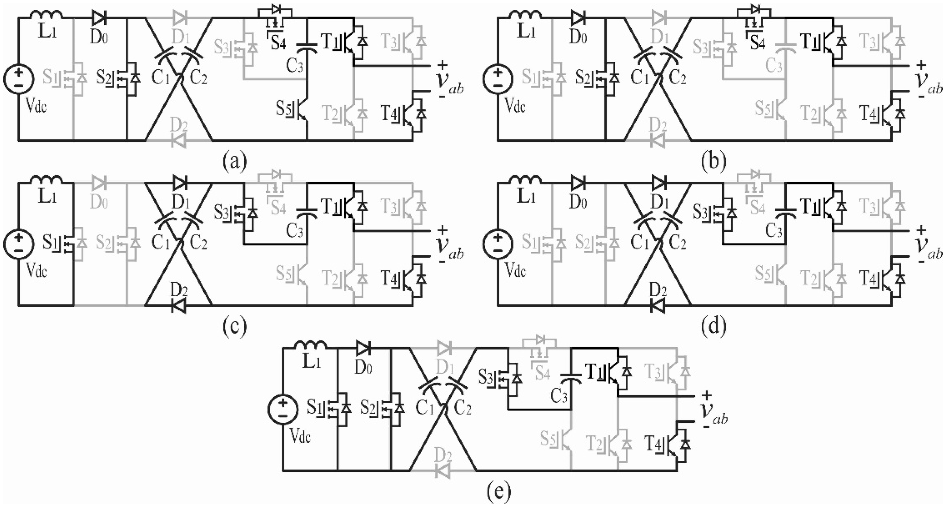
2. Proposed Single-Phase Nine-Level Boost Inverter

Figure 1 shows the proposed single-phase NLBI. As shown in Figure 1, the proposed NLBI consists of a single DC source (Vdc), a conventional boost converter, a switched-diode-capacitor (SDC) circuit [25], a switched-capacitor (SC) circuit [17], an H-bridge circuit, a low-pass filter (LfCf) and a load (R). In the SDC circuit, two capacitors C1 and C2 are discharged in serial when the switch S1 is switched ON. When the switch S1 is switched OFF, two capacitors C1 and C2 are charging by the diodes D1 and D2. In the SC circuit, the capacitor C3 is charged through the body diode of switch S4 when the switch S5 is switched ON and the switch S3 is switched OFF. When the switch S3 is switched ON and the switch S5 is switched OFF, the capacitor C3 is discharged.

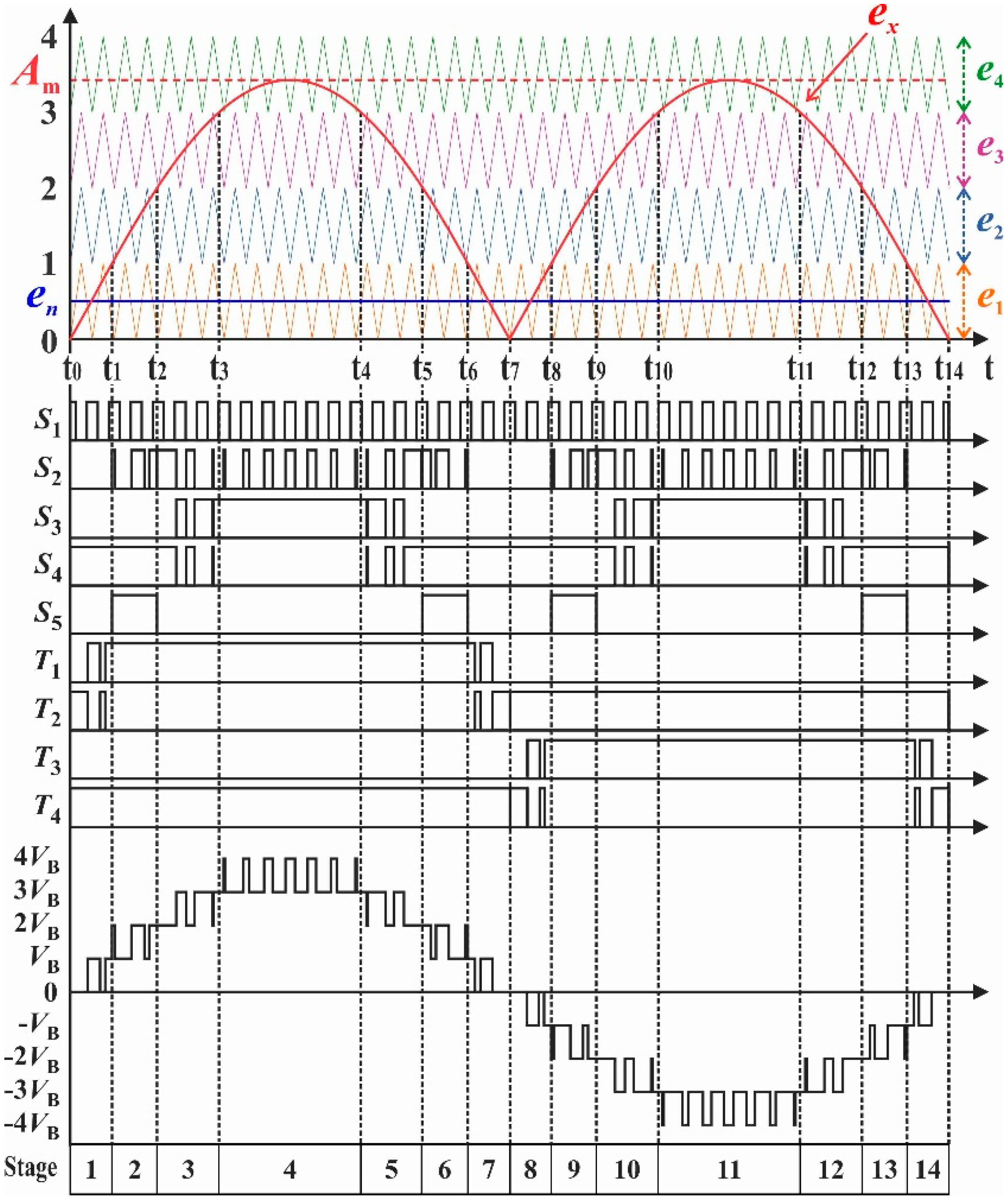
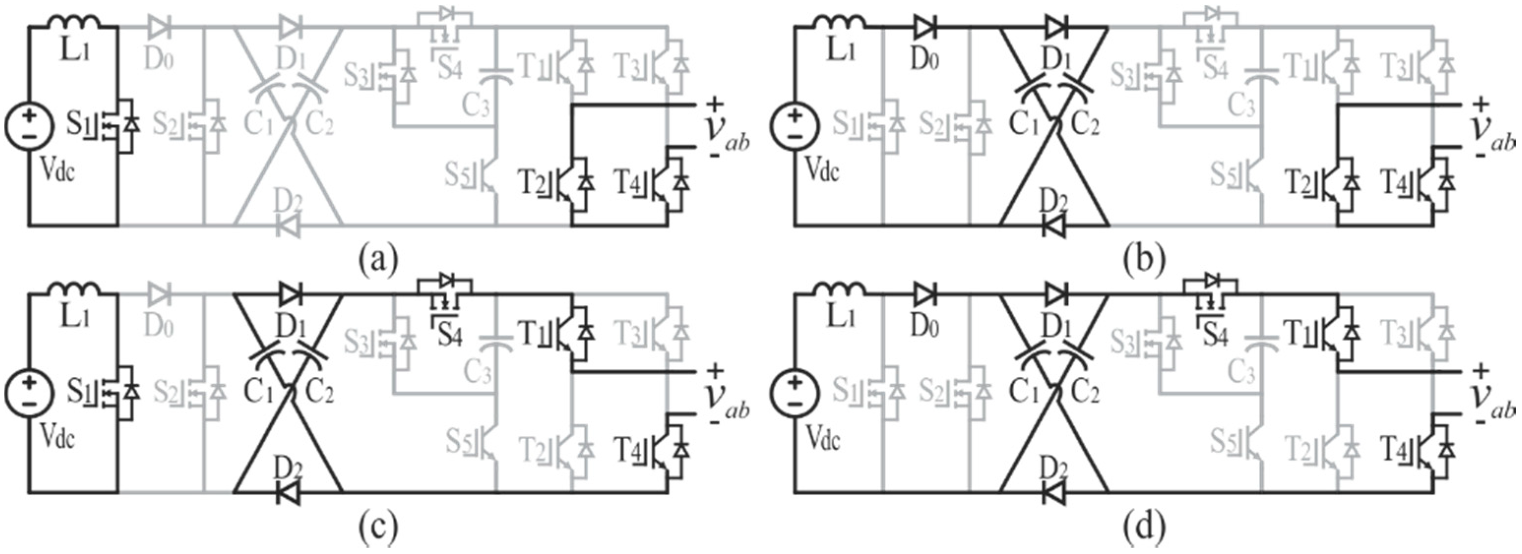
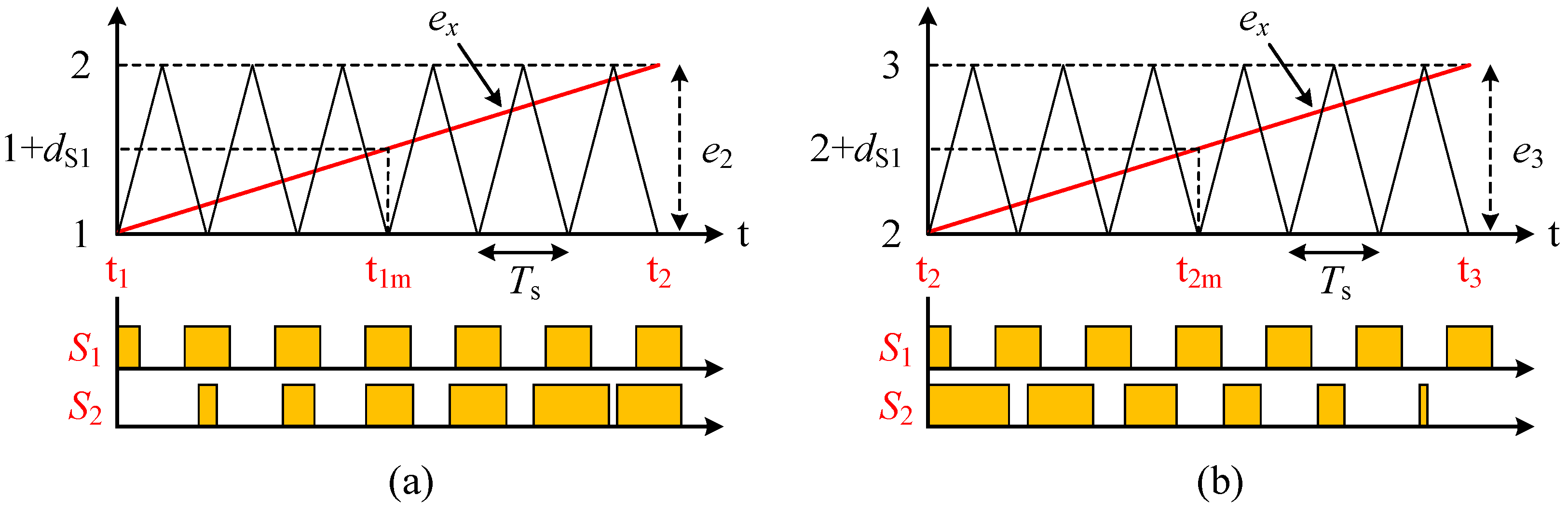
2.1. Operating Principle of the Proposed Inverter

Figure 2 describes the level shift multicarrier-based pulse-width modulation (PWM) scheme for the proposed single-phase NLBI. A control waveform (ex) is compared to four carrier waveforms (e1e4) which these waveforms have the identical phase and amplitude to handle the switches. A constant voltage, en is compared to the carrier voltage e1 to generate a control signal for S1, which works with duty cycle dS1 for each cycle Ts. In Figure 1, VB is the boost voltage value of the boost converter which equals to the collector-emitter voltage of the switch S2. Figure 3 and Figure 4 show the operating states of the proposed NLBI.
The output voltage is positive from t0 to t7 with corresponding to Stages 1–7. Between t7 and t14, the output voltage is negative, corresponding to Stages 8–14. In the positive period from t0 to t7, the circuit operation includes seven stages and nine states (State 1 to State 9, Figure 3 and Figure 4).
Stage 1 (t0t1, Figure 3a–d): When S1 is switched ON, the inductor L1 stores energy from the DC source. If T1 is switched OFF, the output voltage is equal to zero (Vab = 0) as shown in Figure 3a for State 1. If T1 is switched ON, the output voltage is equal to the boost voltage (Vab = VB) as shown in Figure 3c for State 3.
When S1 is switched OFF, the diode D0 is forward-biased, and the inductor L1 is discharged to the capacitors C1 and C2. If T1 is switched OFF, the output voltage is zero (Vab = 0) as shown in Figure 3b for State 2. When T1 is switched ON, the output voltage equals the boost voltage (Vab = VB) as shown in Figure 3d for State 4. The operating duty cycle of the boost inductor in this stage is the duty cycle of switch S1, dS1.
Stage 2 (t1t2, Figure 3c,d and Figure 4a): The switches S5 and T1 are fully switched ON. When S2 is turned ON, whereas S1 is switched OFF, the capacitors C1 and C2 are working in series supplying power to the load. The capacitor C3 is charged by C1 and C2 through S5 simultaneously. As shown in Figure 4a for State 5, the load voltage is equal to twice boost voltage (Vab = 2VB).
When S2 is switched OFF, while S1 is switched ON, the inductor L1 stores energy from Vdc. The capacitors C1 and C2 are working in parallel to feed the load. Although S5 is switched ON in this state, the current from the capacitors C1 and C2 cannot pass through the capacitor C3 because the capacitor C3 voltage is greater than the capacitor C1 and C2 voltages. Consequently, there is no current flow to S5 and the load is connected to the capacitors C1 and C2 in parallel. This state is the same as the State 3 as shown in Figure 3c, the output voltage equals the boost voltage (Vab = VB). The control signal of S5 during this stage can be changed in another way, which is similar to the control signal for S2. To reduce the switching losses, the control signal of S5 is always controlled ON during this stage.
Similarly, when S1 is switched OFF, whereas S5 is turned ON, the output voltage is equal to the boost voltage (Vab = VB), which is the same as the State 4 as shown in Figure 3d.
As shown in Figure 2, the duty cycle of S2 in this stage is gradually increased, while the duty cycle of S1 is fixed at dS1. The time interval of Stage 2 is divided into two subintervals. In the first subinterval (t1t1m, see Figure 5a), the duty cycle of S1 is greater than that of S2. The operating duty cycle of the boost inductor in the first subinterval is dS1. In the second subinterval (t1mt2, see Figure 5a), the duty cycle of S2 is more than that of S1. As a result, the operating duty cycle of the boost inductor in the second subinterval depends on the duty cycle of S2. The average duty cycle of the boost inductor in this sub-stage can be approximated as
d S 2 1 + d S 1 2 ,
The time t1m is calculated as
t 1 m = sin 1 ( 1 + d S 1 A m ) 2 π f o u t ,
where fout and Am are the frequency of the output voltage and the peak amplitude of control waveform ex, respectively.
Stage 3 (t2t3, Figure 4b–d): The switch S3 is complementary to the switch S2. When S3 is switched ON, the load voltage is equal to three times the boost voltage (Vab = 3VB). If S1 is switched ON, the inductor L1 stores energy from Vdc, while the capacitors C1 and C2 working in parallel are connected in series to the capacitor C3 for supplying power to the load as shown in Figure 4c for State 7. When S1 is switched OFF, the capacitors C1 and C2 are charged by the DC voltage source, while the capacitor C3 is still connected in series with the capacitors C1 and C2 as shown in Figure 4d for State 8.
When the switch S2 is switched ON and the switch S3 is switched OFF, the inductor L1 stores energy while the capacitors C1 and C2 are in series for supplying power to the load. From Figure 4b for State 6, it can be seen that the output voltage of the inverter equals to twice boost voltage (Vab = 2VB).
As shown in Figure 2, the duty cycle of S2 in this stage is gradually decreased, while the duty cycle of S1 is fixed at dS1. The time interval of Stage 3 is divided into two subintervals. In the first subinterval (t2t2m, see Figure 5b), the duty cycle of S2 is more than that of S1. The inductor is almost charged during the first subinterval. Therefore, the operating duty cycle of the boost inductor is 1.
In the second subinterval (t2mt3, see Figure 5b), the duty cycle of S1 is greater than that of S2. The operating duty cycle of the boost inductor in the second subinterval is total duty cycle of the switches S1 and S2, we have
d x = d S 1 + d S 2 ,
where dS2 is average duty cycle of the switch S2 in the second subinterval and calculated approximately as (1).
The time t2m is defined as
t 2 m = sin 1 ( 2 + d S 1 A m ) 2 π f o u t ,
Stage 4 (t3t4, Figure 4c–e): When the switches S1, S2 and S3 are switched ON, whereas the switch S5 is switched OFF, the capacitors C1, C2 and C3 are working in series for supplying power to the load. The load voltage is equal to four times the boost voltage (Vab = 4VB) as shown in Figure 4e for State 9. Other states in this stage to reach the output voltage at three times boost voltage are the same as those in Stage 3. In the control method as shown in Figure 2, the duty cycle of S1 is always greater than S2 in terms of time (t3t4) and (t10t11) so that the calculation becomes simpler. Therefore, the following condition is obtained as
d S 1 > A m 3
The operating duty cycle of the boost inductor in Stage 4 is dS1.
Stage 5—(t4t5, Figure 4b–d: the same as Stage 3)
Stage 6—(t5t6, Figure 3c,d and Figure 4a: the same as Stage 2)
Stage 7—(t6t7, Figure 3a–d: the same as Stage 1)
In the negative period from t7 to t14 including seven stages and nine states, the switch T2 is fully switched ON, while T1 is fully switched OFF. The signal T3 is obtained by comparing the carrier e1 and the control waveform ex. The signal T4 is the opposite. All the remaining switches have the same states as in the positive period. The load voltage of the proposed inverter is summarized in Table 2.

2.2. Circuit Analysis of the Proposed Inverter

The circuit analysis is begun with the following assumptions: the capacitors C1 and C2 are equal, the capacitance is large enough to the voltage across the capacitor is constant, and the pairs of diodes–capacitors (D1C1 and D2C2) are symmetrical and balanced. The operating states of the proposed NLBI simplify into two operating modes: charging inductor and discharging inductor. The charging inductor modes are given in Figure 3a–e. These states are controlled by switch S1 and S2, and the inductor L1 is charged at this time.
Assuming that the Tavg is the average time interval of the charging inductor mode during the period Ts, and davg = Tavg/Ts is the average duty cycle of the boost inductor in each period Ts. When S1 or S2 is switched ON, the inductor stores energy as shown in Figure 3a–e for States 1, 3, 5, 6, 7 and 9, respectively. The inductor L1 voltage is:
V L = V d c
When both S1 and S2 switches are switched OFF, the inductor is discharged as shown in Figure 3b,d and Figure 4d for States 2, 4 and 8, respectively. The average time of this mode is (1 − davg)Ts. The following equations are obtained as
{ V L = V d c V B V B = V C 1 = V C 2
Because the average voltage crossing the inductor during a period of Ts is zero, from (6) and (7), the boost voltage is calculated as
V B = 1 1 d a v g V d c
The boost factor of the NLBI is determined as
B = V B V d c = 1 1 d a v g .
From the analysis of the proposed NLBI in Section 2. The operating duty cycle of the boost inductor is summarized as
d L 1 = { d S 1 t 0 t < t 1 m and t 3 t < t 4 0.5 ( 1 + d S 1 ) t 1 m t < t 2 1 t 2 t < t 2 m 0.5 ( 1 + d S 1 ) t 2 m t < t 3 ,
where
t 2 = sin 1 ( 2 A m ) 2 π f o u t ,   t 3 = sin 1 ( 3 A m ) 2 π f o u t
The influence of the operating states of S1 and S2 on the duty cycle of the circuit is not the same in each operating state. However, the operation of S1 and S2 is repeated after a quarter cycle of the output cycle. In one-four time interval of the output voltage time period, the average duty cycle of the boost inductor is calculated as
d a v g = d S 1 + 2 ( 1 d S 1 ) ( t 3 + t 2 m t 2 t 1 m T o u t ) ,
where Tout = 1/fout is the period of the output voltage. The voltage gain (G) is expressed as
G = AmB

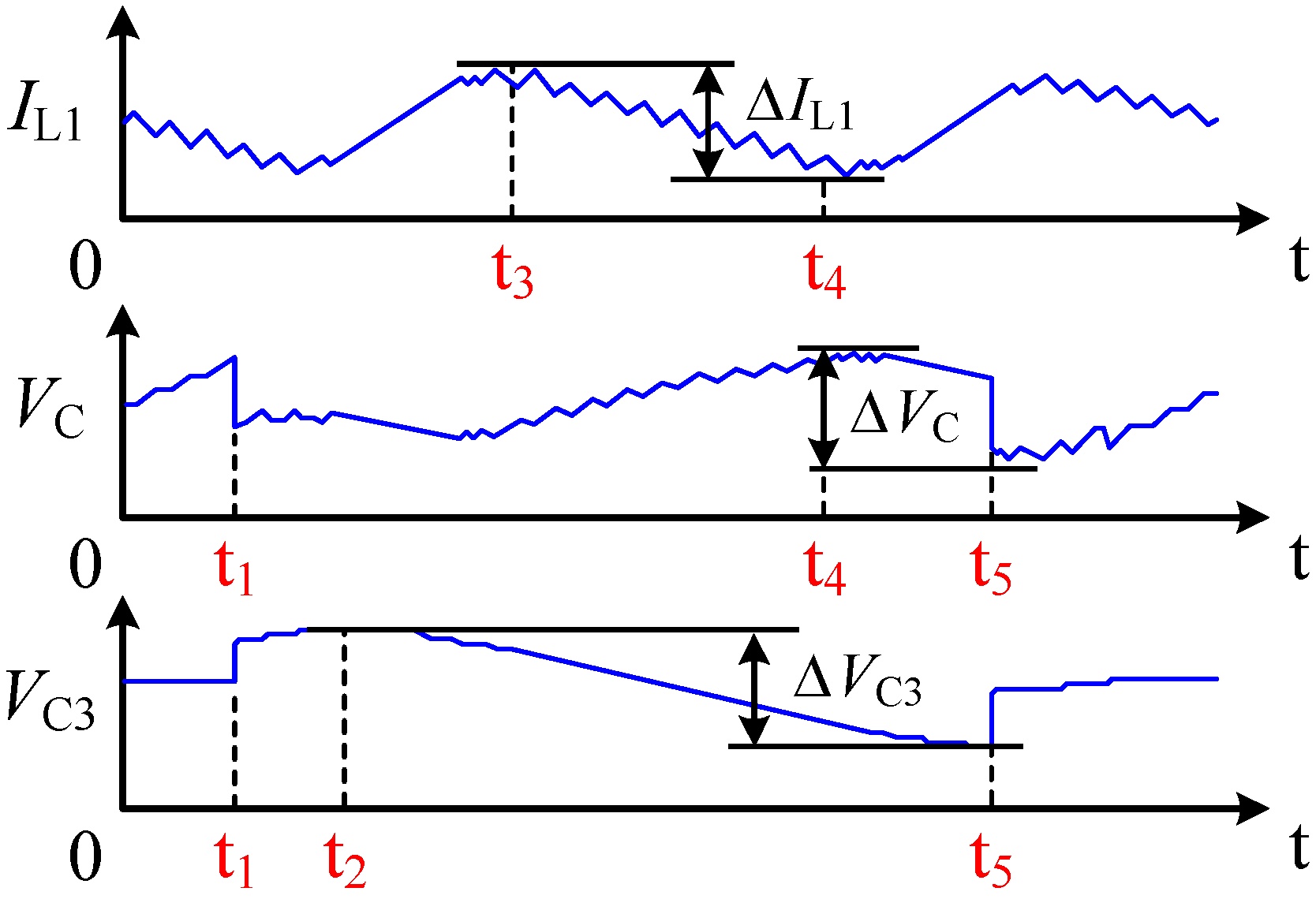
3. Inductor and Capacitor Selections

Figure 6 shows the inductor current and capacitor voltage waveforms in the positive output voltage. In Figure 6, the voltage waveforms on capacitors C1 and C2 are the same and equal to VC.
Assuming that the output power (POUT) equals the input power, the average input current can be calculated as
I L 1 = P O U T V d c
The current ripple of the inductor is defined as
Δ I L 1 t 3 t 4 d i L 1 d t d t = 1 L 1 t 3 t 4 [ d S 1 V d c + d S 1 ( V d c V C ) ] d t = d S 1 V d c ( 2 B ) L 1 ( t 4 t 3 ) ,
where
t 4 = π sin 1 ( 3 A m ) 2 π f o u t
The inductance is determined by the current ripple factor KL as
K L = Δ I L 1 I L 1 = d S 1 V d c 2 ( 2 B ) P O U T L 1 ( t 4 t 3 ) .
The inductance is selected as
L 1 d S 1 V d c 2 ( 2 B ) P O U T K L ( t 4 t 3 ) .
The capacitance Ci (i = 1, 2 and 3) can be calculated based on the voltage ripple on the capacitors Ci. In this case, the capacitor Ci is determined by the maximum voltage ripple at k% of the maximum voltages of the capacitors. The capacitors C1 and C2 are charged when the switches S1 and S2 are switched OFF. The capacitors C1 and C2 are discharged in the remaining cases of the switches S1 and S2. The capacitor C3 is charged when the switch S5 is switched ON, whereas it is discharged when the switch S5 is switched OFF.
Assuming that the output load has the power factor (cosφ) of 1, the longest discharging term of the capacitor C3 in the proposed NLBI is between t2 and t5 as shown in the Figure 6. The maximum discharge amounts Q3 of the capacitor C3 is:
Q 3 I o ( t 4 t 3 ) + I o sin ( 2 π f o u t t 3 ) ( t 3 t 2 ) ,
where Io is the amplitude the output current. When the Q3 is less than k% of the maximum charge of C3, the capacitance C3 needs to meet the condition as:
C 3 Q 3 k V C 3 .
The reduction of the capacitor C1 or C2 voltages is equal to the incensement of the capacitor C3 voltage at times t1 and t5 as shown in Figure 6. At this time, the charging of capacitor C3 affects the ripple of capacitors C1 or C2. Because the capacitor C3 voltage is twice the capacitor C1 voltage, the ripple of capacitor C1 will be larger than that of the capacitor C3. Therefore, the capacitance of selected capacitors C1 and C2 will be greater than or equal to the capacitance of capacitor C3.

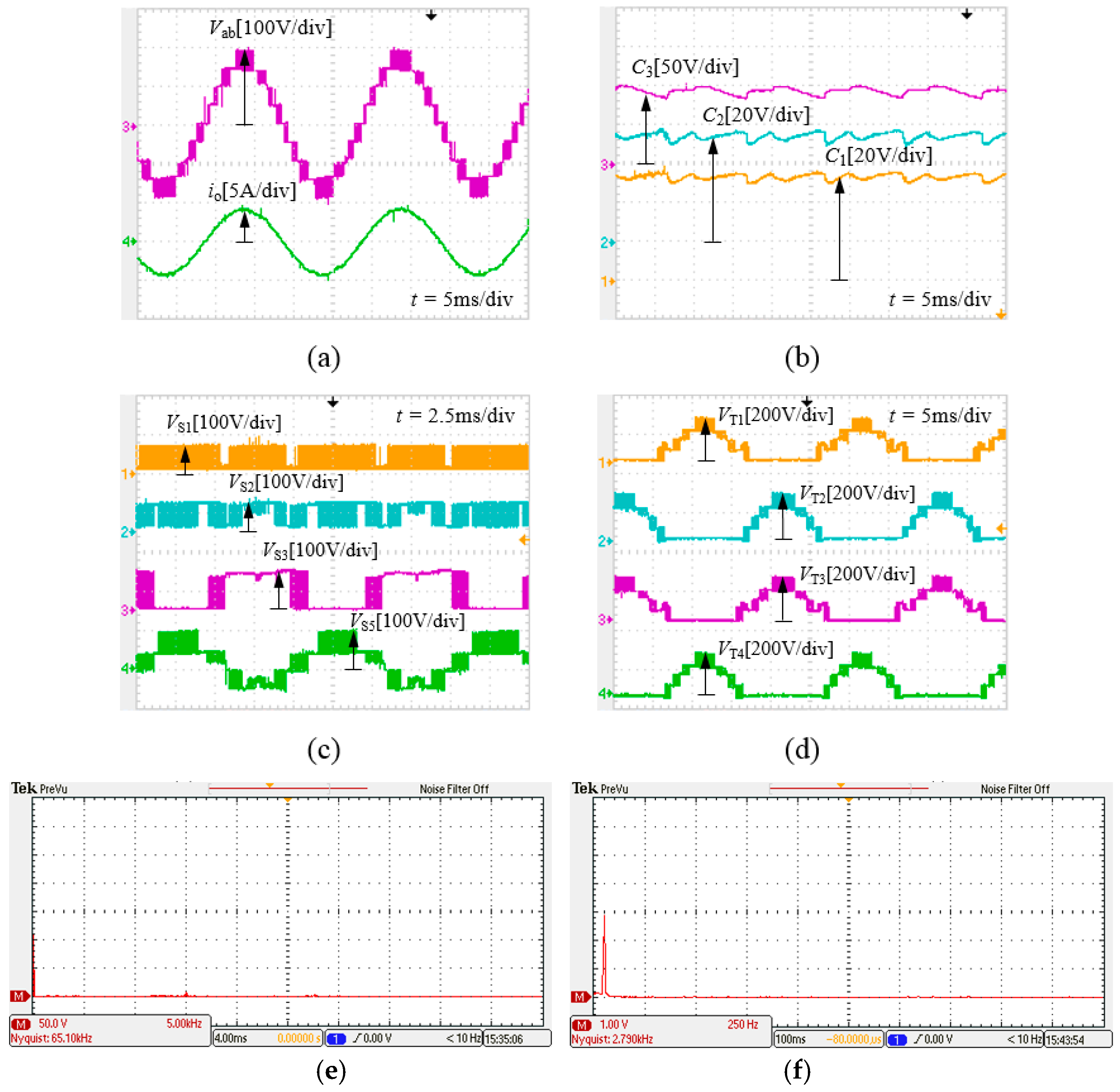
4. Simulation and Experimental Results

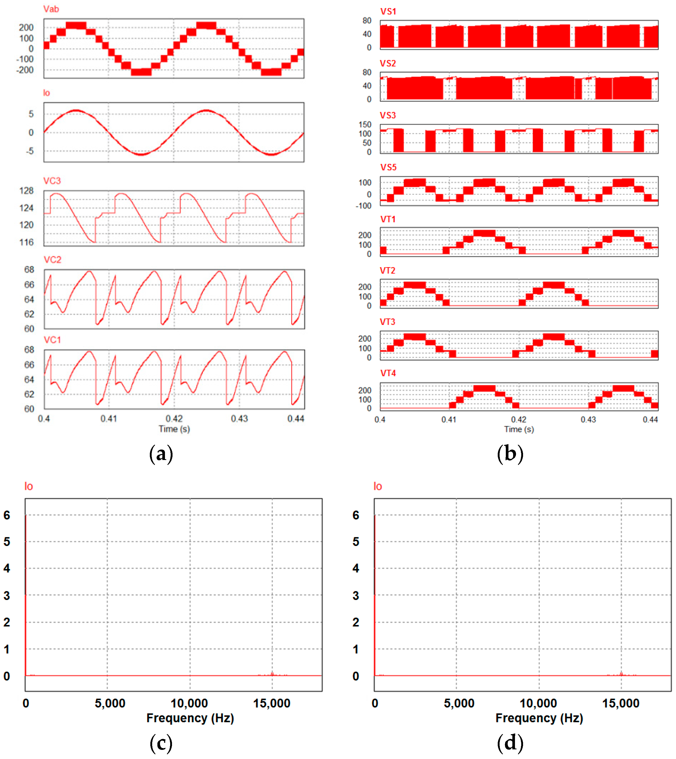
4.1. Simulation Results

PSIM 9.1.1 software was studied to verify the operational principle of NLBI. The input voltage is set at Vdc = 24 V and the simulation power is 680 W. The inductor L1 = 2 mH. The capacitors C1 = C2 = C3 = 2200 µF. The switching frequency is 15 kHz. Connect the resistor R = 36 Ω and use the inductor capacitor (LC) filter Lf = 2.5 mH, Cf = 1 µF.
Figure 7 shows the simulation results of the NLBI when Am = 3.4, dS1 = 0.4. Figure 7a shows the nine-level output voltage Vab, the load current io and the ripple voltage of the capacitors (VC1, VC2, VC3). Figure 7b shows the voltage waveform of the switches S1, S2, S3, S5 and the voltage waveform of the H-bridge switches T1T4. The capacitor voltages VC1, VC2 and VC3 are boosted to 65 V from the input voltage of 24 V. The maximum voltage of the switches S1 and S2 is 65 V, while the maximum voltage of the switches S3 and S5 is 130 V. The maximum voltage on the switches T1T4 is 260 V. Figure 7c,d show the harmonic spectrum of the output voltage Vab and the load current io in the frequency domain, respectively. As seen in Figure 7c, the main component appears around the frequency of 15 kHz and 30 kHz.

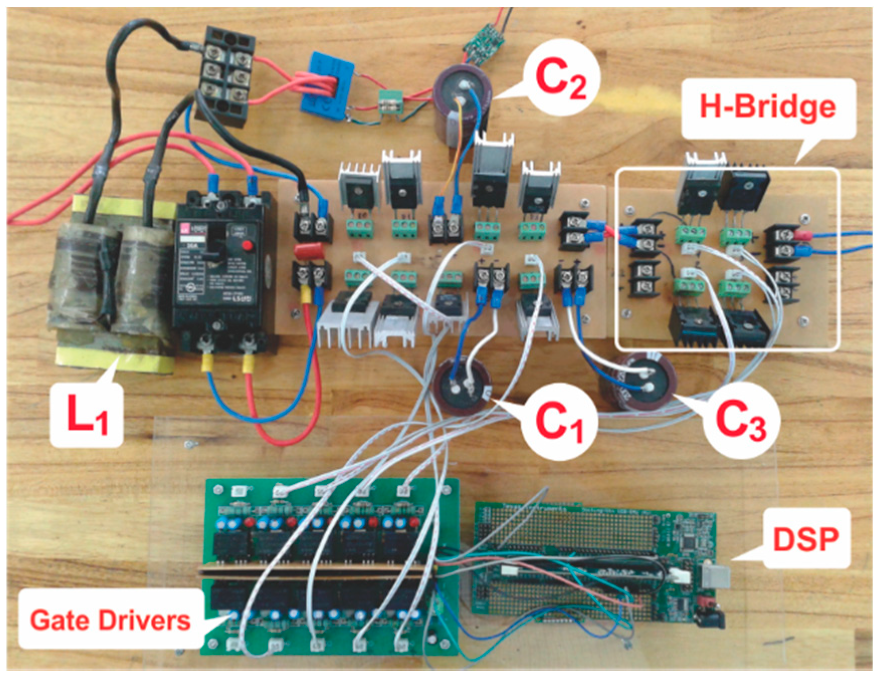
4.2. Experimental Results

A 350 W prototype based on TMS320F28335 DSP was built as shown in Figure 8. The input DC voltage is 24 V. The output voltage is 110 Vrms/50 Hz. The specifications of the experiment are given in Table 3. The switches S1, S2, S3 and S4 are 47N60C3 MOSFETs, whereas the other switches are G40N120 IGBTs. Note that the switch S5 refers to MOSFET. Because the MOSFET without body diode is not available in the laboratory, a G40N60 IGBT without body diode is used in the experiment.
Figure 9 shows the experimental results of the NLBI when Am = 3.4, dS1 = 0.4. Figure 9a shows the waveforms of the output voltage Vab and the load current io. As shown in Figure 9a, the output voltage has nine levels. As shown in Figure 9b, the capacitors C1, C2 and C3 voltage are boosed to 52.2 V, 52.2 V and 92.5 V from the input voltage of 24 V, respectively. Figure 9c,d show the experiment results of switches S1, S2, S3, S5 voltage and switches T1T4 voltage of the H-bridge circuit, respectively. Figure 9e,f shows the harmonic spectrum of the output voltage, Vab and harmonic spectrum of output current.
Table 4 lists the theoretical, simulation and experimental values of B, VC1, VC2 and VC3 when dS1 = 0.4, Vdc = 24 V, and Am = 3.4. It can be seen from Table 4 that the simulation value is approximately equal to the theoretical value, which shows the correctness of the theoretical analysis. Moreover, the experimental value is less than that of corresponding theoretical value because the power losses are found in the experimental prototype. The voltage on capacitor C3 is not equal to the sum of capacitors C1 and C2 because the discharge time of capacitor C3 is longer associated with the losses on switches S2, S4, S5 when charging capacitor C3.

5. Conclusions

In this paper, a nine-level boost inverter which decreases the number of switching elements by switching the capacitor in series and in parallel has been suggested. The main advantage of the NLBI in comparison with the traditional topology is that the number of switches is reduced with using only a single DC voltage source. Therefore, the economic benefits from the proposed inverter come from the size and cost reduction of the inverter system. The output voltage expression and the parameter calculation are presented. Moreover, a control method based on the PWM technique is proposed for the proposed inverter. Finally, the simulation and experimental results of the NLBI are presented to validate its viability, well-performance, and effectiveness of suggested modulation strategy. The proposed inverter is suitable for low-power applications, where a low input voltage from renewable energy sources such as solar cell, fuel cell and battery needs to convert to a single-phase AC source.

Author Contributions

All authors contributed equally to this work and all authors have read and approved the final manuscript.

Funding

This research was funded by the Korea Institute of Energy Technology Evaluation and Planning (KETEP) and the Ministry of Trade, Industry& Energy (MOTIE) of the Republic of Korea grant number 20184010201650 and the APC was funded by KETEP and MOTIE.

Acknowledgments

This work was supported by the Korea Institute of Energy Technology Evaluation and Planning (KETEP) and the Ministry of Trade, Industry& Energy (MOTIE) of the Republic of Korea (NO. 20184010201650).

Conflicts of Interest

The authors declare no conflicts of interest.

Nomenclature

Ampeak amplitude of control waveform ex
Bboost factor
CHBcascade H-bridge
davgaverage duty cycle of the boost inductor in each period Ts
dL1duty cycle of the boost inductor
dS1duty cycle generated by switch S1
dS2duty cycle generated by switch S2
dxduty cycle generated by switch S1 and S2
enconstant voltage
excontrol waveform
foutoutput frequency
FCflying-capacitor
Gvoltage gain
ioload current
Ioamplitude of output current
IL1average input current
ΔIL1current ripple of the inductor
KLcurrent ripple factor of the inductor
MImultilevel inverter
NLBInine-level boost inverter
NPCneutral-point-clamped
PWMpulse-width modulation
SCswitched-capacitor
SCMIswitched-capacitor multilevel inverter
SDCswitch-diode-capacitor
Tavgaverage time interval of the charging inductor mode during the period Ts
Tsperiod time
Vaboutput voltage
VBboost voltage
Vdcdc source
VLinductor L1 voltage

References

  1. Abu-Rub, H.; Holtz, J.; Rodriguez, J.; Baoming, G. Medium-Voltage Multilevel Converters-State of the Art, Challenges, and Requirements in Industrial Applications. IEEE Trans. Ind. Electron. 2010, 57, 2581–2596. [Google Scholar] [CrossRef]
  2. Soeiro, T.B.; Kolar, J.W. The new high-efficiency hybrid neutral-point-clamped converter. IEEE Trans. Ind. Electron. 2013, 60, 1919–1935. [Google Scholar] [CrossRef]
  3. Dargahi, S.; Babaei, E.; Eskandari, S.; Dargahi, V.; Sabahi, M. Flying-capacitor stacked multicell multilevel voltage source inverters: Analysis and modelling. IET Power Electron. 2014, 7, 2929–2987. [Google Scholar] [CrossRef]
  4. Zha, X.; Xiong, L.; Gong, J.; Liu, F. Cascaded multilevel converter for medium-voltage motor drive capable of regenerating with part of cells. IET Power Electron. 2014, 7, 1313–1320. [Google Scholar] [CrossRef]
  5. Tran, T.T.; Nguyen, M.K. Cascaded five-level quasi-switched-boost inverter for single-phase grid-connected system. IET Power Electron. 2017, 10, 1896–1903. [Google Scholar] [CrossRef]
  6. Rodriguez, P.; Bellar, M.D.; Munoz-Aguilar, R.S.; Busquets-Monge, S.; Blaabjerg, F. Multilevel-clamped multilevel converters (MLC2). IEEE Trans. Power Electron. 2012, 27, 1055–1060. [Google Scholar] [CrossRef]
  7. Husev, O.; Roncero-Clemente, C.; Romero-Cadaval, E.; Vinnikov, D.; Stepenko, S. Single phase three-level neutral-point-clamped quasi-Z-source inverter. IET Power Electron. 2015, 8, 1–10. [Google Scholar] [CrossRef]
  8. Teymour, H.R.; Sutanto, D.; Muttaqi, K.M.; Ciufo, P. A novel modulation technique and a new balancing control strategy for a single-phase five-level ANPC converter. IEEE Trans. Ind. Appl. 2015, 51, 1215–1227. [Google Scholar] [CrossRef]
  9. Ajami, A.; Oskuee, M.; Mokhberdoran, A.; Bossche, A.V.D. Developed cascaded multilevel inverter topology to minimize the number of circuit devices and voltage stresses of switches. IET Power Electron. 2014, 7, 459–466. [Google Scholar] [CrossRef]
  10. Tsang, K.; Chan, W. Single DC source three-phase multilevel inverter using reduced number of switches. IET Power Electron. 2014, 7, 775–783. [Google Scholar] [CrossRef]
  11. Wang, K.; Li, Y.; Zedong, Z.; Xu, L. Voltage balancing and fluctuation-suppression methods of floating capacitors in a new modular multilevel converter. IEEE Trans. Ind. Electron. 2013, 60, 1943–1954. [Google Scholar] [CrossRef]
  12. Najafi, E.; Yatim, A.H.M. Design and implementation of a new multilevel inverter topology. IEEE Trans. Ind. Electron. 2012, 59, 4148–4154. [Google Scholar] [CrossRef]
  13. Hinago, Y.; Koizumi, H. A single-phase multilevel inverter using switched series/parallel dc voltage sources. IEEE Trans. Ind. Electron. 2010, 57, 2643–2650. [Google Scholar] [CrossRef]
  14. Rahim, N.A.; Chaniago, K.; Selvaraj, J. Single-phase seven-level grid-connected inverter for photovoltaic system. IEEE Trans. Ind. Electron. 2011, 58, 2435–2443. [Google Scholar] [CrossRef]
  15. Hinago, Y.; Koizumi, H. A switched-capacitor inverter using series/parallel conversion with inductive load. IEEE Trans. Ind. Electron. 2012, 59, 878–887. [Google Scholar] [CrossRef]
  16. Raman, R.S.; Ye, Y.; Cheng, E.W.K. Switched-capacitor multilevel inverters for high frequency ac microgrids. In Proceedings of the 2017 IEEE Applied Power Electronics Conference and Exposition (APEC), Tampa, FL, USA, 26–30 March 2017; pp. 2559–2564. [Google Scholar] [CrossRef]
  17. Barzegarkhoo, R.; Kojabadi, H.M.; Zamiry, E.; Vosooghi, N.; Chang, L. Generalized structure for a single phase switched-capacitor multilevel inverter using a new multiple dc link producer with reduced number of switches. IEEE Trans. Power Electron. 2016, 31, 5604–5617. [Google Scholar] [CrossRef]
  18. Tsunoda, A.; Hinago, Y.; Koizumi, H. Level- and phase-shifted PWM for seven-level switched-capacitor inverter using series/parallel conversion. IEEE Trans. Ind. Electron. 2014, 61, 4011–4021. [Google Scholar] [CrossRef]
  19. Ye, Y.; Cheng, K.W.E.; Liu, J.; Ding, K. A step-up switched-capacitor multilevel inverter with self-voltage balancing. IEEE Trans. Ind. Electron. 2014, 61, 6672–6680. [Google Scholar] [CrossRef]
  20. Babaei, E.; Gowgani, S.S. Hybrid multilevel inverter using switched-capacitor units. IEEE Trans. Ind. Electron. 2014, 61, 4614–4621. [Google Scholar] [CrossRef]
  21. Ngo, B.B.; Nguyen, M.K.; Kim, J.H.; Zare, F. Single-phase multilevel inverter based on switched-capacitor structure. IET Power Electron. 2018, 11, 1858–1865. [Google Scholar] [CrossRef]
  22. Liu, J.; Cheng, K.W.E.; Ye, Y. A cascaded multilevel inverter based on switched-capacitor for high-frequency ac power distribution system. IEEE Trans. Power Electron. 2014, 29, 4219–4230. [Google Scholar] [CrossRef]
  23. Sun, X.; Wang, B.; Zhou, Y.; Wang, W.; Du, H.; Lu, Z. A single dc source cascaded seven-level inverter integrating switched-capacitor techniques. IEEE Trans. Ind. Electron. 2016, 63, 7184–7194. [Google Scholar] [CrossRef]
  24. Gao, F. An enhanced single phase step-up five-level inverter. IEEE Trans. Power Electron. 2016, 31, 8024–8030. [Google Scholar] [CrossRef]
  25. Hou, S.; Chen, J.; Sun, T.; Bi, X. Multi-input step-up converters based on the switched-diode-capacitor voltage accumulator. IEEE Trans. Power Electron. 2016, 31, 381–393. [Google Scholar] [CrossRef]
Figure 1. Proposed single-phase nine-level boost inverter (NLBI) topology.
Energies 12 00394 g001
Figure 2. Modulation method for the proposed single-phase NLBI.
Energies 12 00394 g002
Figure 3. Operation states in the positive output voltage period of the proposed NLBI. (a) State 1, (b) State 2, (c) State 3 and (d) State 4.
Energies 12 00394 g003
Figure 4. Operation states in the positive output voltage period of the proposed NLBI (continuous). (a) State 5, (b) State 6, (c) State 7, (d) State 8 and (e) State 9.
Energies 12 00394 g004
Figure 5. Operational analysis of switches S1 and S2 in the interval of (a) Stage 2 and (b) Stage 3.
Energies 12 00394 g005
Figure 6. Inductor current ripple and capacitors voltage ripple.
Energies 12 00394 g006
Figure 7. Simulation results of the proposed NLBI when dS1 = 0.4. The waveforms from top to bottom: (a) nine-level output voltage Vab, load current io, capacitors C3C1 voltage; (b) switches S1, S2, S3, S5 voltage and switches T1T4 voltage of H-bridge circuit, (c) harmonic spectrum of nine-level output voltage and (d) harmonic spectrum of load current.
Energies 12 00394 g007
Figure 8. A laborotary prototype of single-phase NLBI.
Energies 12 00394 g008
Figure 9. Experimental results of NLBI when Am = 3.4, dS1 = 0.4 and Vdc = 24 V. The waveforms from top to bottom: (a) Output voltage Vab, output current io inverter; (b) capacitors C3, C2, C1 voltages; (c) voltage of switches VS1, VS2, VS3, VS5; (d) voltage of switches VT1, VT2, VT3, VT4; (e) harmonic spectrum of the nine-level output voltage; and (f) harmonic spectrum of output current.
Energies 12 00394 g009
Table 1. Advantages and disadvantages of multilevel inverters with reduced switch count.
TopologyLiteratureAdvantagesDisadvantages
Series-connected DC voltage sourcesProposed in Reference [12]
  • Reduce switching losses
  • Number of output voltage levels depends on the number of DC sources
  • Buck voltage
Switched serial/parallel DC voltage sourcesProposed in Reference [13]
  • Simple topology
  • Input sources can be integrated in both parallel and series
  • Complex switching pattern
  • Increase conductive losses
  • Buck voltage
Additional boost converterProposed in References [14,24]
  • Single source
  • Boost voltage
  • Capacitor imbalance is very likely to occur
  • Two-stage conversion
Series/parallel connectionProposed in References [15,18]
  • Single source
  • Boost voltage
  • Large number of switches
Based on switched capacitorProposed in References [16,17,19,20,21]
  • Self-balancing in capacitor voltage
  • Voltage boost capability
  • Reduce switch count but increase number of diodes
  • High capacitor current stress
Cascaded multilevel inverterProposed in References [22,23]
  • Reduce voltage stress on H-bridge switches
  • Boost voltage
  • Only show in high-frequency AC output voltage [20]
  • Using separate dc source
Table 2. Different Switching, Capacitor, and Inductor States of the Proposed NLBI.
StateStageON DiodesON SwitchesCapacitor StateInductor L1 StateOutput Voltage
C1C2C3
11, 7 S1, S4, T2, T4III+0
21, 7D0, D1, D2S4, T2, T4++I0
31, 2, 6, 7D1, D2S1, S4, T1, T4I+VB
41, 2, 6, 7D0, D1, D2S4, T1, T4++IVB
52, 6D0S2, S4, S5, T1, T4++2 VB
63, 5D0S2, S4, T1, T4I+2 VB
73, 4, 5D1, D2S1, S3, T1, T4+3 VB
83, 4, 5D0, D1, D2S3, T1, T4++3 VB
94D0S1, S2, S3, T1, T4+4 VB
108, 14 S1, S4, T2, T4III+0
118, 14D0, D1, D2S4, T2, T4++I0
128, 9, 13, 14D1, D2, D3S1, S4, T2, T3I+−VB
138, 9, 13, 14D0, D1, D2, D3S4, T2, T3++I−VB
149, 14D0, D3S2, S4, S5, T2, T3++2 VB
1510, 12D0, D3S2, S4, T2, T3I+2 VB
1610, 11, 12D1, D2S1, S3, T2, T3+3 VB
1710, 11, 12D0, D1, D2S3, T2, T3++3 VB
1811D0S1, S2, S3, T2, T3+4 VB
Here “I”, “+” and “−” refer to the idle, charging and discharging states, respectively.
Table 3. Operating Parameters for the Proposed Inverter.
ParameterValue
Power rating350 W
Input voltage (Vdc)24 V
Output voltage (Vab)110 Vrms/50 Hz
Carrier ware frequency (fs)15 kHz
InductorsL12 mH
Lf1 mH
Capacitors C1, C2, C32200 µF/200 V
Cf1 µF
Power switchesS1, S2, S3, S447N60C3
S5G40N60
T1, T2, T3, T4G40N120
Diodes (D0, D1, D2, D3)DSEI60-06A
Gate drivesTLP250 (Photo-coupler)
Table 4. Comparison between Calculated, Simulated and Experimental Values.
Data fromVab (V)ΔVab (%)BVC1 and VC2 (V)VC3 (V)
Theory156.202.765130
Simulation152.22.562.764.6122.3
Experiment11029.572.1752.292.5
Here “ΔVab” is the percentage change between experiment and simulation versus theory.

