Article

Impact of Wide-Bandgap Technology on Renewable Energy and Smart-Grid Power Conversion Applications Including Storage

by
Alberto Castellazzi
1,*,
Emre Gurpinar
2,
Zhenyu Wang
3,
Abdallah Suliman Hussein
3 and
Pablo Garcia Fernandez
4
1
Faculty of Engineering, Kyoto University of Advanced Science, Kyoto 615-8577, Japan
2
Electrical and Electronics Systems Research Division, Oak Ridge National Laboratory, Oak Ridge, TN 37830, USA
3
Power Electronics, Machines and Control (PEMC) Group, University of Nottingham, Nottingham NG7 2RD, UK
4
Department of Electrical Engineering and Computer Science (DIEECS), University of Oviedo, 33203 Gijon, Spain
*
Author to whom correspondence should be addressed.
Energies 2019, 12(23), 4462; https://doi.org/10.3390/en12234462
Submission received: 17 October 2019 / Revised: 11 November 2019 / Accepted: 18 November 2019 / Published: 22 November 2019
(This article belongs to the Special Issue Advanced Materials/Devices for Power Electronics)

Abstract

:
Wide-bandgap (WBG) semiconductor devices are making their way into large-volume applications, including pivotal domains of societal infrastructure such as sustainable energy generation and conversion. Presented for a long time mainly as a synonym of high-temperature electronics, hands-on experience has highlighted a number of gains that can be drawn from this technology even when used as a straightforward drop-in substitute of silicon in established applications and field-proven designs. Incremental in nature, these gains enable interesting progress beyond state-of-the-art forms, which, though not corresponding to the full exploitation of the potential of this technology, are oftentimes sufficient to justify its adoption. With particular reference to renewable energy power conversion and solid-state transformation, in the context of transport applications and incorporating a storage device, this paper reports on the understanding generated over the past few years and points out some specifically tailored technology and circuit design requirements to ensure overall beneficial impact of the adoption of WBG technology.

1. Introduction

Wide-bandgap (WBG) semiconductor devices are key enablers in the evolution of power electronic technologies, specifically for their capability to jointly deliver an enhanced efficiency, power density, and reliability of electrical energy conversion equipment. Over the past few years, the quality of commercial transistors has been improved to a level comparable to established silicon technology, and engineering samples have been made available in an increasingly broad range of voltage and current ratings. Presently, silicon carbide (SiC) MOSFETs and gallium nitride (GaN) HEMTs are being used as the primary switches in pivotal societal application areas, such as energy generation and distribution, transportation, and industrial drives. GaN is the only competitor of Si (MOSFETs) for low-voltage ratings, indicatively from 100 to 400 V. GaN and SiC both become of interest for applications relying on devices with a 650 V rating, which include power supplies, residential photo-voltaic and wind power conversion, automotive, and small actuators. When used in multilevel inverter topologies, input voltages in excess of 1 kV can also be used with transistors in this voltage class. GaN HEMTs presently have an edge for very to ultra-high switching frequency (fs) applications, where miniaturization is a major asset (e.g., portable appliances, infotainment, parts of the automotive electronics). SiC MOSFETs are the preferred choice when avalanche ruggedness is required or beneficial (e.g., automotive, avionics, actuation). At higher voltage levels, SiC MOSFETs compete alone with Si IGBTs. Presently, widespread agreement exists, that SiC MOSFETs are very competitive with and can outperform Si IGBTs surely up to the 3.3 kV voltage class; beyond that rating, SiC is still of interest, but bipolar-type devices (e.g., SiC BJTs) are being earnestly considered [1].
In the aforementioned application domains, the most urgent interest and need is to assess the incremental gain that can be derived from deploying devices as a drop-in replacement for Si components in consolidated circuit architectures and design solutions. Novel developments and concepts aiming at maximum exploitation of the superior device characteristics represent a parallel line of investigation with a longer-term impact target. So, for instance, while WBG has been long anticipated and presented essentially as a synonym of high-temperature electronics, the requirement and realistic opportunity to actually fully exploit the higher temperature capability of WBG over Si remains confined, for a number of reasons discussed more in detail in the final section, to niche markets and application segments. The many-fold switching speed and switching frequency (fs) capabilities, while amply demonstrated at the research level, find little immediate use in large-volume, established applications, where a modest increment is presently regarded as the most realistic short-term target (indicatively, a factor of 4 is presently judged sufficient to justify the higher initial cost of the technology), as it does not require major re-design of existing and field-proven solutions.
From that same perspective, this paper reports on the learning done in recent years in some representative applications selected from the renewable energy applications domain (PV and wind). The findings clearly indicate that significant incremental benefits (not disruptive) can be drawn from WBG technology already as a drop-in replacement for Si, even with conventional standardized packaging solutions [1,2,3,4,5,6]. The higher initial price of the semiconductors is counter-balanced by savings in the filter elements and cooling, as well as by the possibility to do without free-wheeling diodes even in higher-voltage applications. The issue of reduced performance at low-load conditions emerges as a connoting feature of WBG technology operated at high frequencies, which requires careful and dedicated attention, with a perspective shift in power converter performance assessment from power to energy efficiency, taking into account the most probable operational load conditions [7,8]. Incremental improvement on standard power module assembly technology is proven sufficient to enable significant application gains, up to and including the 3.3 kV voltage class [9,10]. Specific aspects of common-mode capacitance reductions and robust module designs that incorporate statistical analyses of the realistic spread of a device’s electro-thermal parameters are highlighted as the main key requirements in the framework of incremental, as opposed to disruptive, progress beyond state-of-the-art technology [11,12].

2. Renewable Energy Inverters

As a first case study, a single-phase, 3-level, active neutral point clamped (ANPC) inverter was considered. The inverter was specifically intended for residential grid-connected PV applications and had a rating of 5 kW, with input voltages ranging between 400 and 700 V. The reference fs value for the industrial product based on Si IGBTs was 16 kHz.

2.1. Inverter Performance and Power Density Trade-Off

Because of the current and voltage rating involved, 650 V discrete transistors in the TO247 package were chosen for the main switches. This enabled a straightforward benchmark within the same exact power cell design with all available technologies [3,4,5], including Si IGBTs, SiC MOSFETs, and GaN HEMTs (gate injection type, GIT). The highest performance was achieved with GaN, with a small margin over SiC mainly because of the smaller parasitic capacitances and better switching, whereas both GaN and SiC decidedly outperformed Si. The maximum gain in efficiency at the reference frequency of 16 kHz was above 2% over the whole output power range, with a peak value in excess of 3%, and an at least 10-fold increase in fs was enabled without real penalty on efficiency at a heat-sink temperature of 60 to 90 °C. Figure 1a illustrates the gain that can be made in reducing the output filter size (and weight) when the inductor is operated under identical conditions, as illustrated in Figure 1b, which shows the overall output current over one period of the fundamental output AC frequency (50 Hz here) as well as the detailed ripples for three values of fs and, correspondingly, changing inductor designs. The penalty on efficiency for an increase from 16 to 128 kHz amounted to about 2% at medium-load values, bringing the efficiency curve to correspond to the one for Si at 16 kHz. Clearly of interest, these results represent a validated hyperbolic relation between fs and inductor values, requiring an 8-fold increase of the former to reduce the latter by a factor of 3. Pushing the frequency higher does not bring much in terms of subsequent size and weight reduction, and operation above 200 kHz calls for novel magnetic materials and design approaches in order to yield high performances.

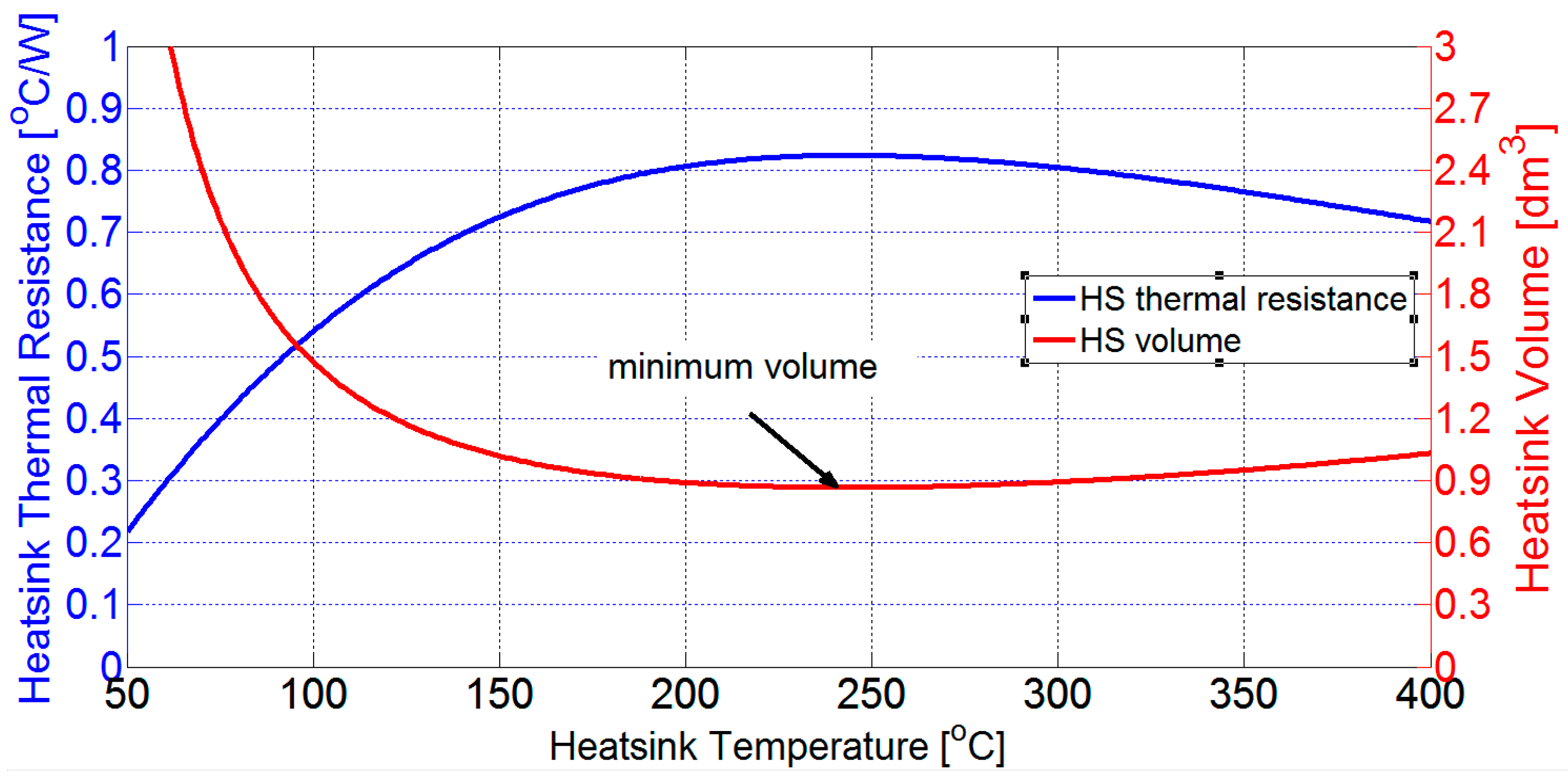
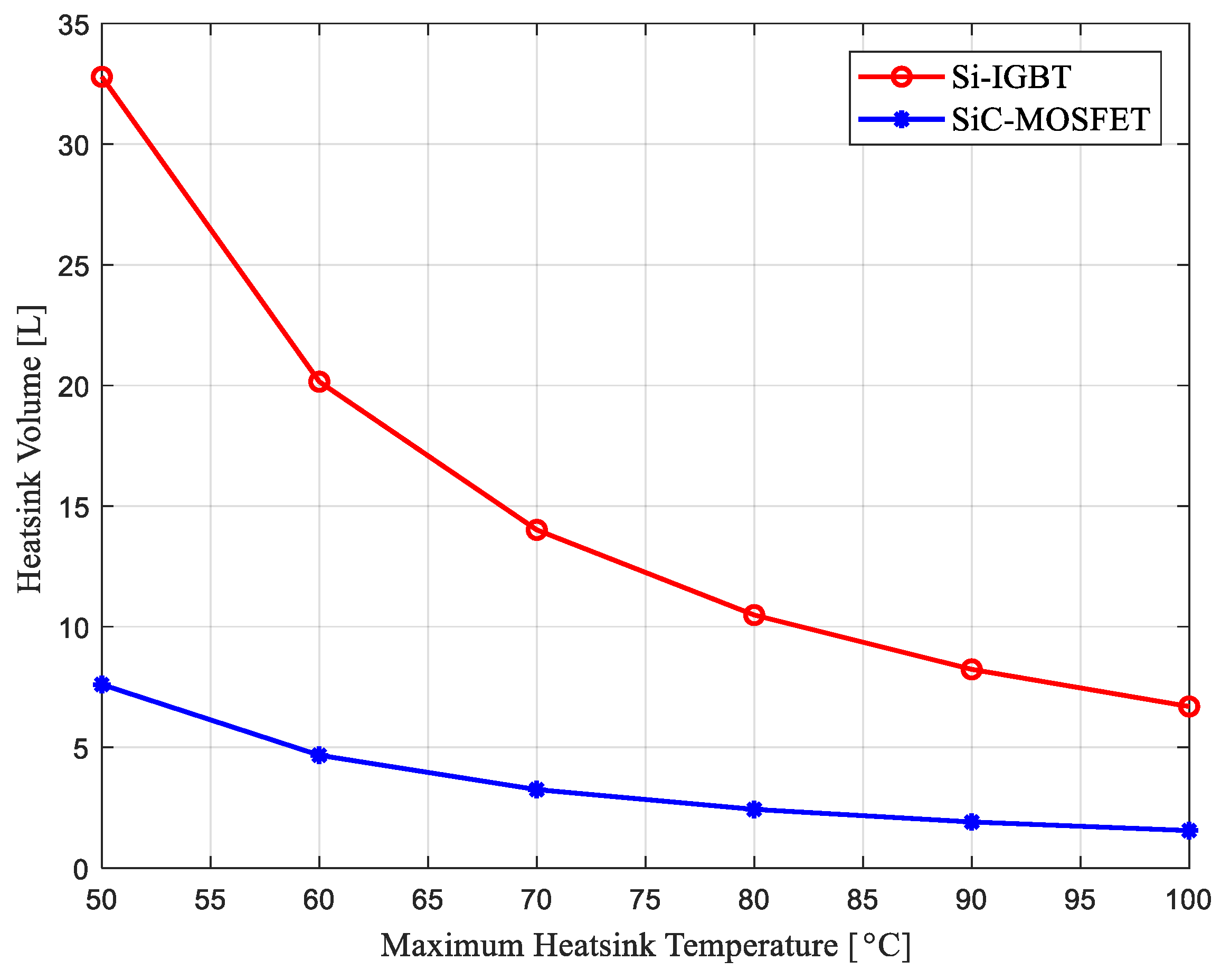
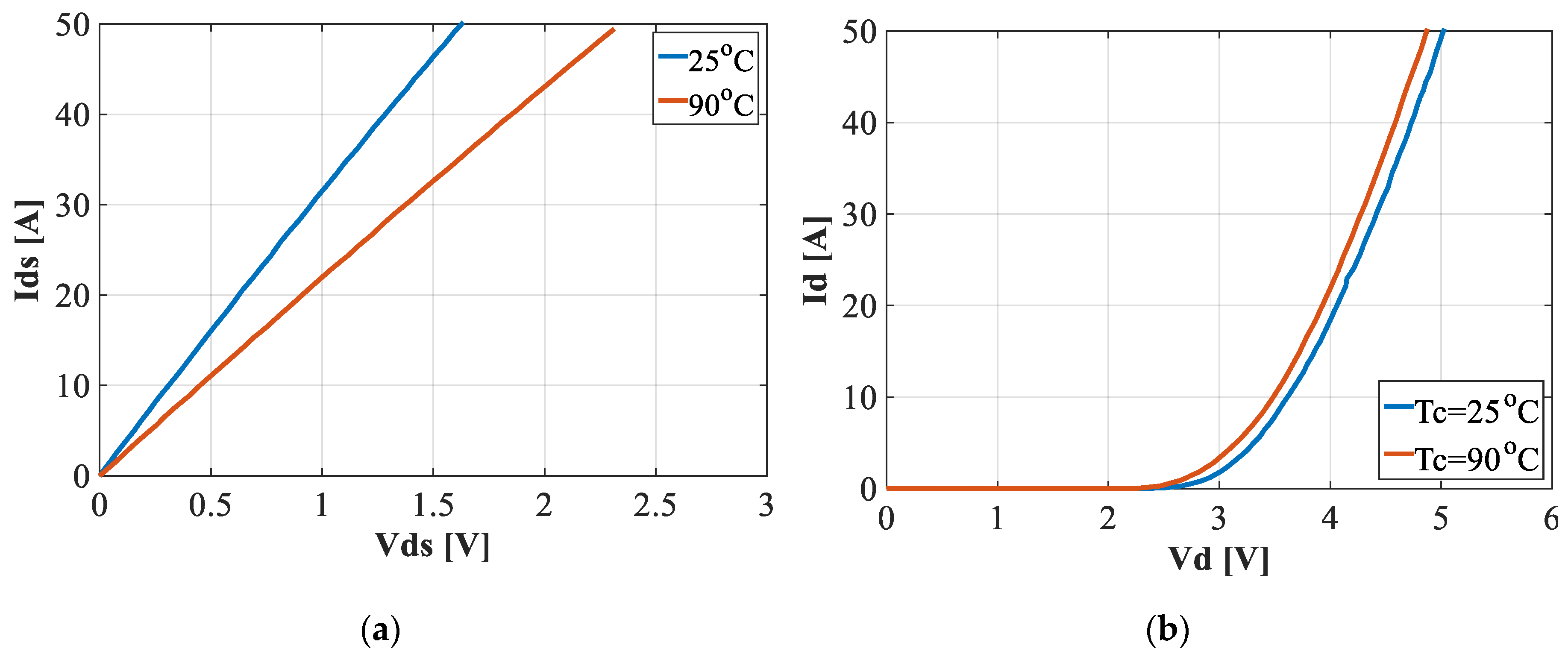
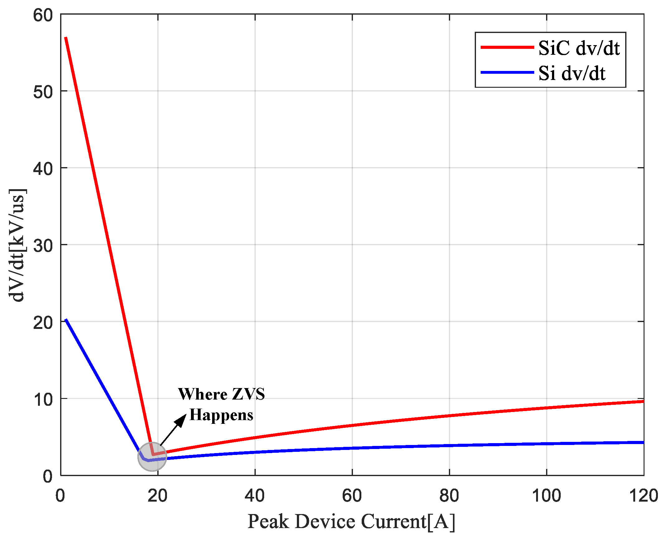
2.2. Higher-Temperature Capability Exploitation

Thus, it becomes of interest to also explore the possibility offered by higher-temperature capabilities and stable device characteristics in further improving the overall power density. Referring to a fully passive heat-sink design, varying shrinking capabilities were pointed out as a function of fs and target heat-sink temperatures (that is, the device’s ambient temperature) at maximum load, which need to be regarded as an interrelated pair of variables for optimum system design. Figure 2a,b shows that the minimum total volume (mainly contributed by heat-sink and filter elements) was achieved for an fs value of 30 kHz, when the target heat-sink temperature at full load was 50 °C. On the other hand, if an increase to 80 °C is accepted, then the optimum point was at around 70 kHz. The overall volume in the second case was about 1.7 times less than in the first case.
To conclude the study, analytical semiconductor devices and heat-sink models were used for a preliminary assessment of the maximum heat-sink temperature up to which a reduction of the heat-sink can be achieved. Figure 3 shows the results. On the left vertical axis is the required thermal resistance to ensure that the steady-state temperature is in accordance with the target; on the right vertical axis is the corresponding heat-sink volume. The results indicate that an optimum point was reached at around 250 °C. Beyond this value, the power losses become so high that the heat-sink volume needs to be increased again to reduce the thermal resistance. The models underlying these analytical results were validated up to 125 °C; thus, validation over a broader range is still needed to confirm the result. Should it be confirmed that a temperature value around 250 °C represents an optimum, that would be an important shift in the perspective about the need to design very high temperature electronics packaging to make the most of WBG technology. A temperature of 250 °C is an incremental target value fully within reach of mainstream interconnected and packaging technologies, and it could be a realistic midterm target also for passive component technology development, whose progress in recent years has undoubtedly lagged over semiconductors and has partly limited full temperature capability exploitation in Si applications as well.

2.3. Multilevel Solutions and Higher-Voltage Rating Devices: Tranfer to High-Power Applications

In view of the above results, the impact of WBG as a drop-in replacement for Si devices on the power converter performance and power density can be surely asserted to be of a significant incremental value, but not quite as disruptive as probably generally anticipated. From this point of view, and also motivated from the expectation of SiC MOSFET technology being competitive up to, indicatively, 3.3–4.5 kV over Si, multilevel inversion solutions are gaining momentum in relation to the successful deployment of WBG solutions. Applying 3.3 kV devices with a de-rating of 50% on the maximum operational voltage (as is common practice in many established Si applications), a 3-level solution would allow input voltages of up to about 3 kV; a 5-level solution would bring the value up to 6.5 kV. As higher supply voltages and switching frequencies are conditional to the actual development capability of upcoming high-profile applications (e.g., hybrid and full electric aircrafts; larger-capacity renewable energy plants), multilevel inversion is expected to take on an increasingly central and strategic role in assisting the more widespread and pervasive adoption of WBG devices. A key facet of this particular aspect is the possibility, within a relatively recent and developing area of research, to optimize both the inverter architecture and the switching sequence/modulation strategy to the peculiarities of WBG devices. Figure 4a shows an original 5-level hybrid topology, the efficient and dense architecture (EDA5), specifically devised and operated with SiC and power scalability in the range from tens up to some hundreds of kilowatts in mind [13]. Figure 4b shows the profile of compact hardware for a single-phase prototype implemented with a rating of 15 kW and the output voltage and current waveforms. The topology is suitable for use with devices in all voltage classes, from 650 V to 3.3 kV, and exploits the free-wheeling capability of the MOSFETs body-diode, without any additional diode, to yield very competitive performances in terms of efficiency, power density, and harmonic signature.
Figure 5a shows the output characteristics of a recent generation of 3.3 kV MOSFET (ca. 7 × 7 mm2 die size), measured at two different temperature values. Figure 5b shows its body-diode characteristics. These results simultaneously highlight a good temperature stability of the technology and the need to implement synchronous rectification for the best performance, limiting conduction of the body-diode to the commutation dead-times.

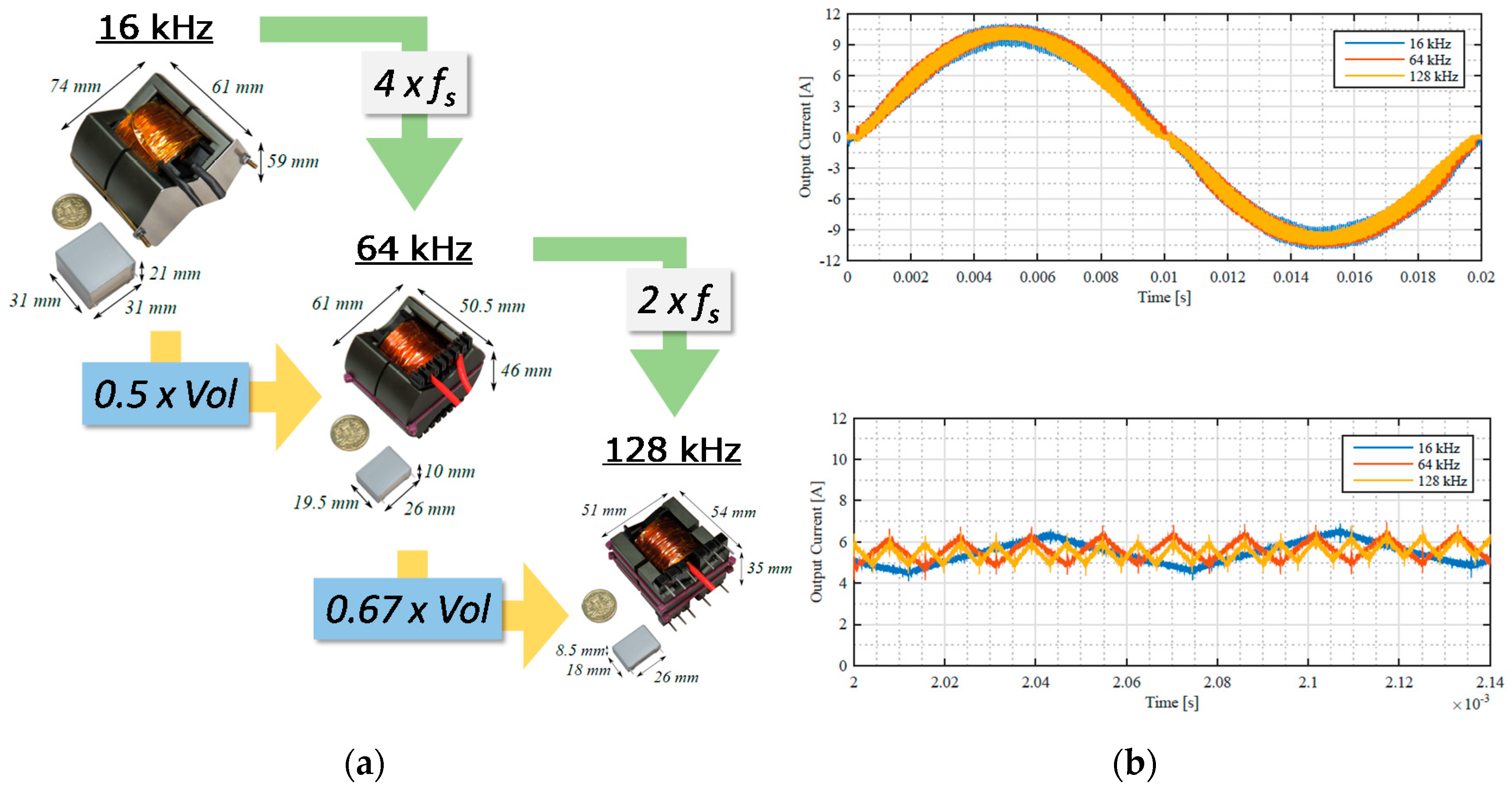
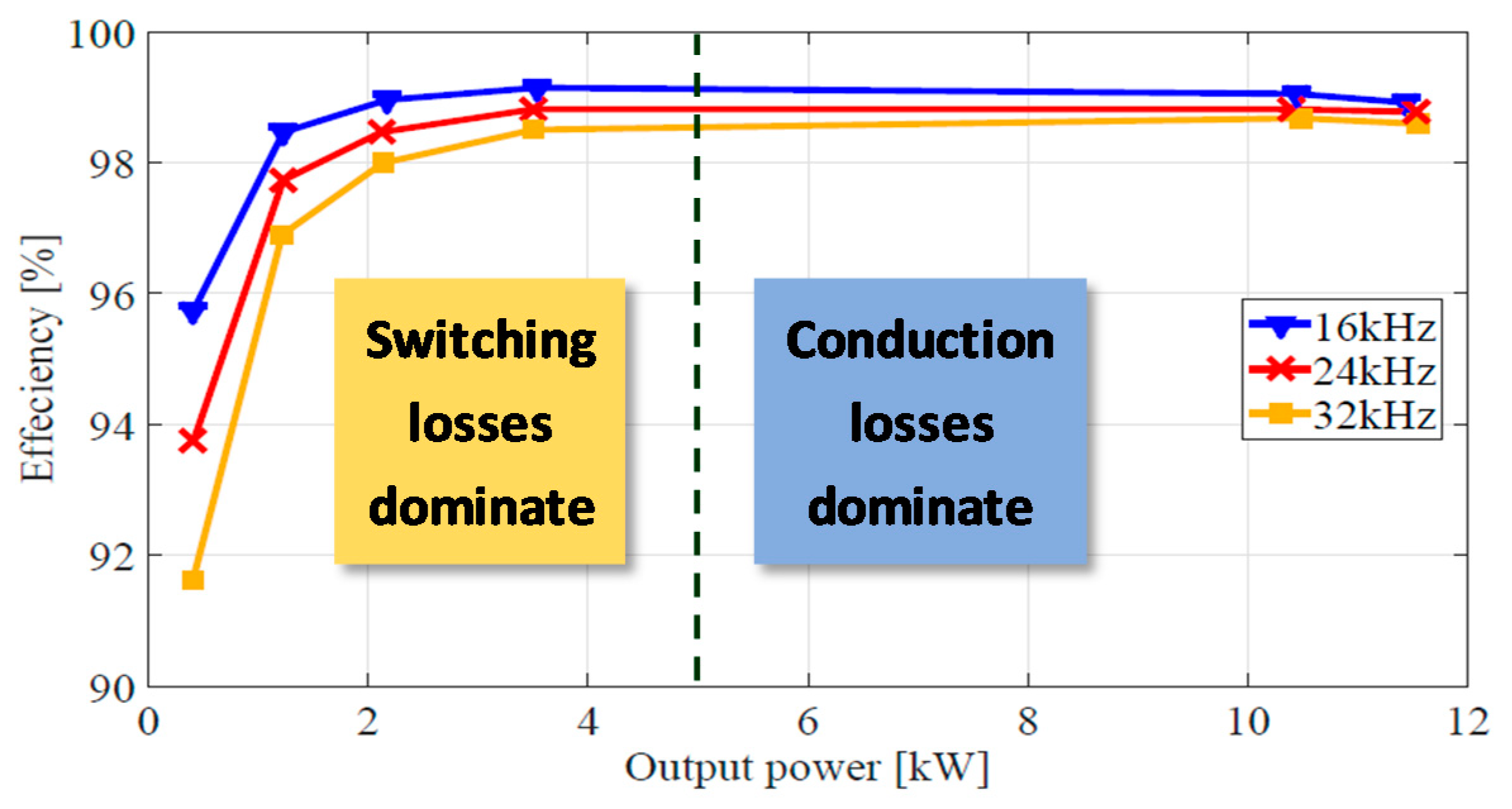
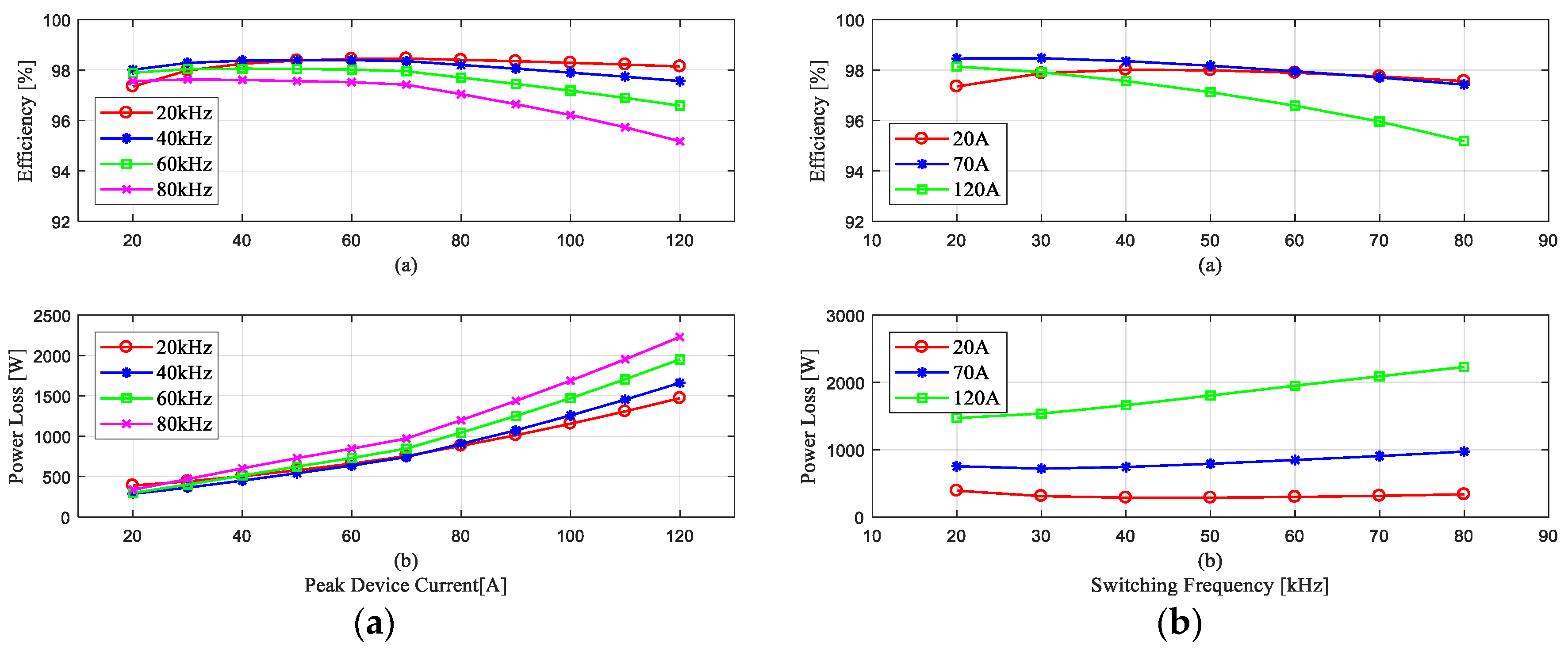
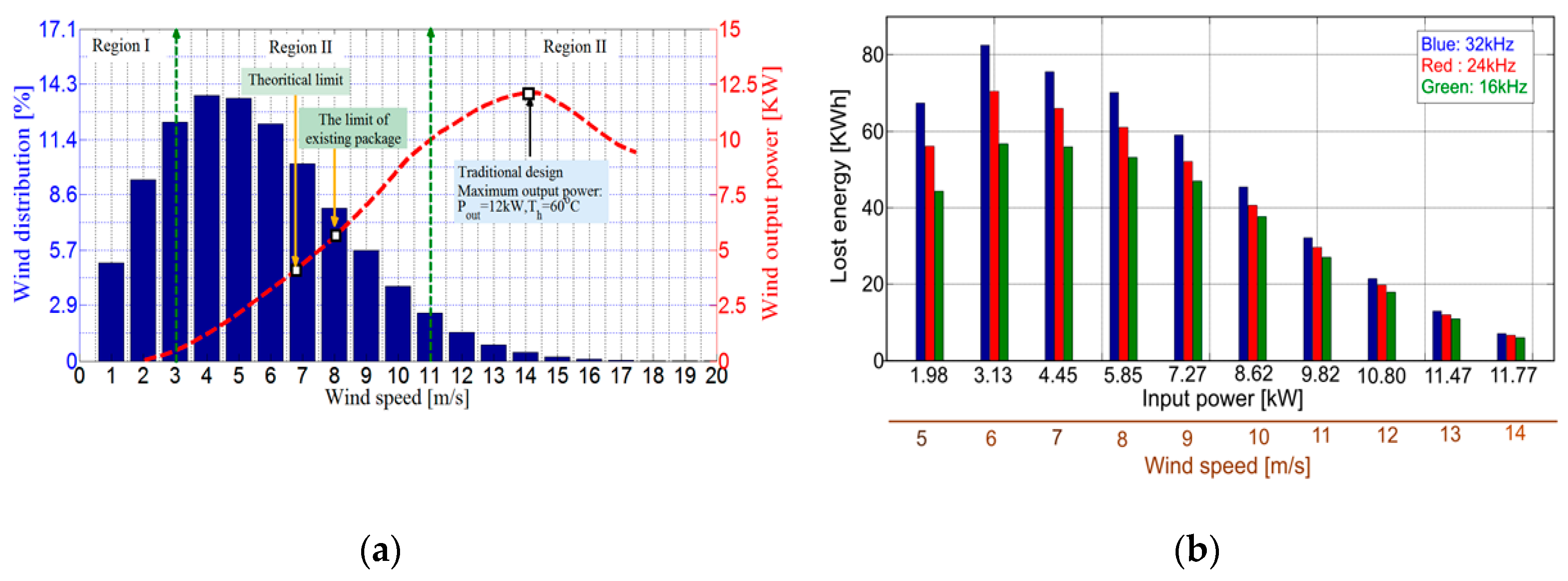
2.4. Low-Load Efficiency Penalty at High Switching Frequencies: Energy Versus Power Efficiency Optimisation

Finally, as the benefits of higher fs values have been demonstrated, one related issue needs to be highlighted as a specific feature of WBG technology. Figure 6 reports the efficiency of a 12 kW wind-turbine inverter measured for three different values of fs, with only small increases between values. As can be seen, the change in fs hardly had an effect on the higher output power portion of the graph. However, the low-load operation was severely penalized by even a modest increase. This issue is not trivial. A very large proportion of power converters (probably the vast majority) actually spend most of their operational time working at low-load conditions. Figure 7a shows the measured wind distribution and corresponding wind-turbine output power for a given geographic location. Even though the turbine is rated for 12.5 kW, its most frequent operational condition was closer to 2.5 kW. Thus, if energy efficiency, as opposed to power efficiency, is taken into account, then the indication is clear: it is the low-load efficiency drop that determines the highest energy waste (Figure 7b). Such a situation is representative of many applications, which can draw important benefits from the adoption of WBG technology, including trains, hybrid/electric cars, industrial drives, and air conditioners. The overall cumulated energy waste from all of these applications can be a very important fraction of the total usage in a given geographical area or country. So, the problem needs tackling, and it has started to be addressed with growing attention within the specialist community worldwide.
The issue has already found attention in dedicated research efforts, which successfully proposed the use of load-dependent variable frequency switching schemes, coupled with variable inductor design to boost low-load performance while still complying with harmonic performance requirements (THD and TCC) [7,8,14]. However, because of an added complication with the close-loop control and stability of the inverter, presently, alternative solutions based on a modular assembly with load-dependent, dynamic equivalent, semiconductor area scaling are being pursued.

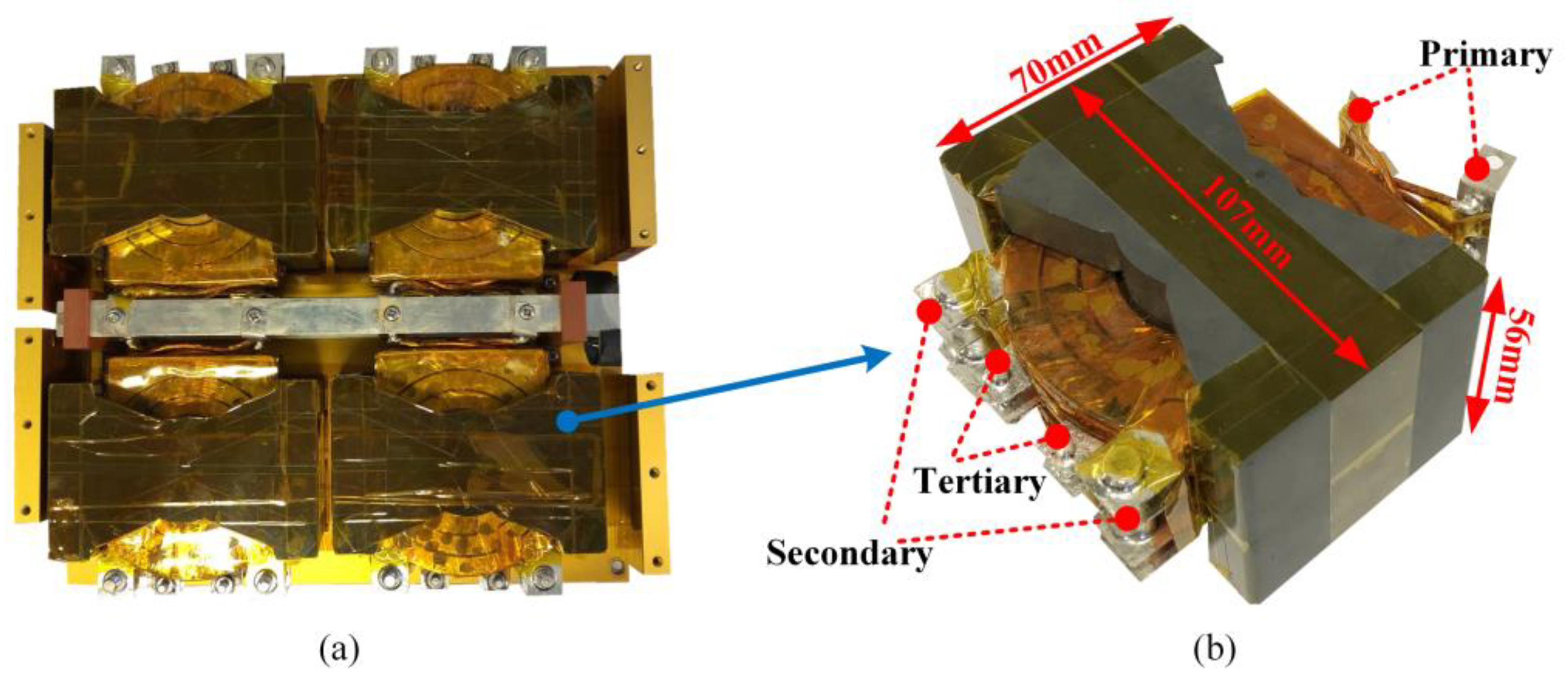
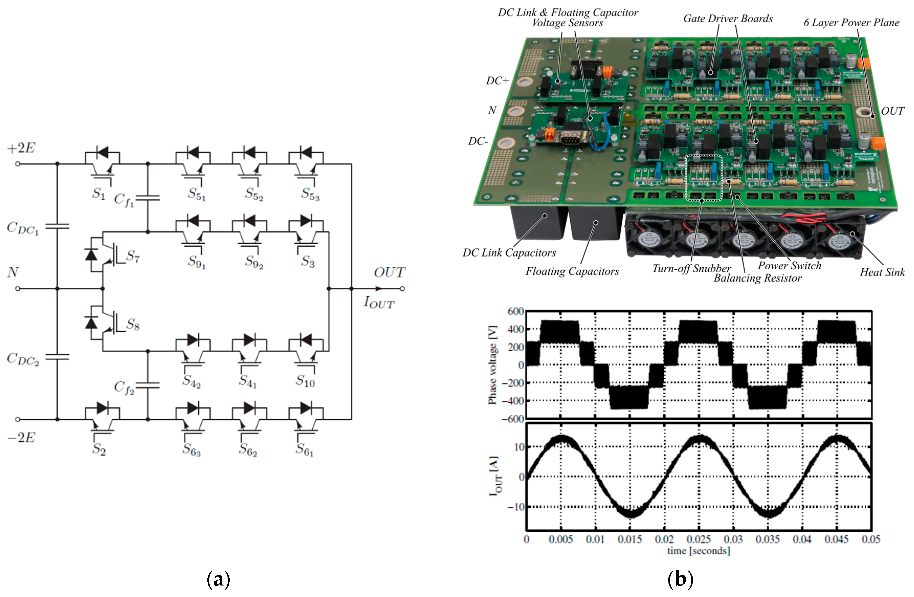
3. Solid-State Transformer (3-Port Dual-Active Bridge DC-DC Converter)

The second case study refers to a DC-DC converter used within a solid-state transformer used in transport applications, where the issue of trading electrical efficiency for gravimetric and volumetric power density is particularly sensitive [15,16].

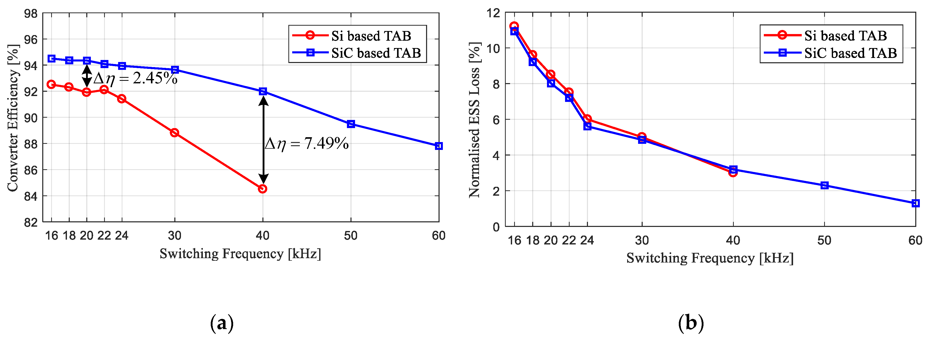
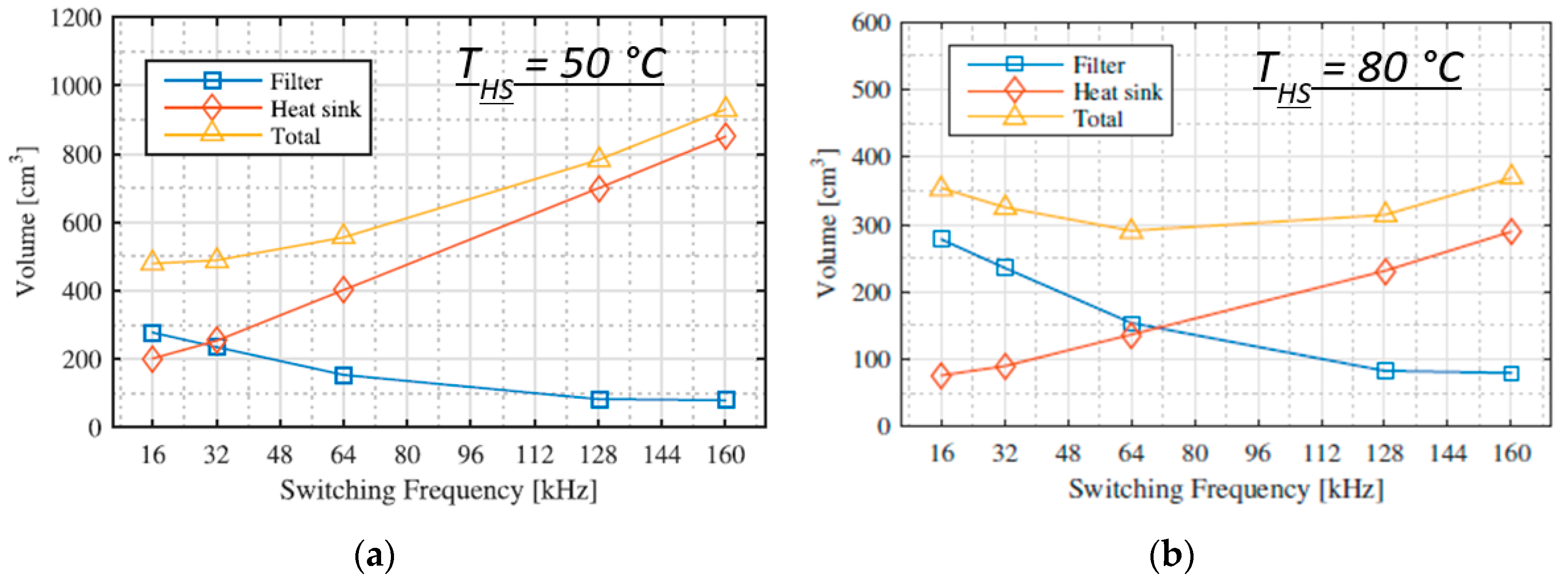
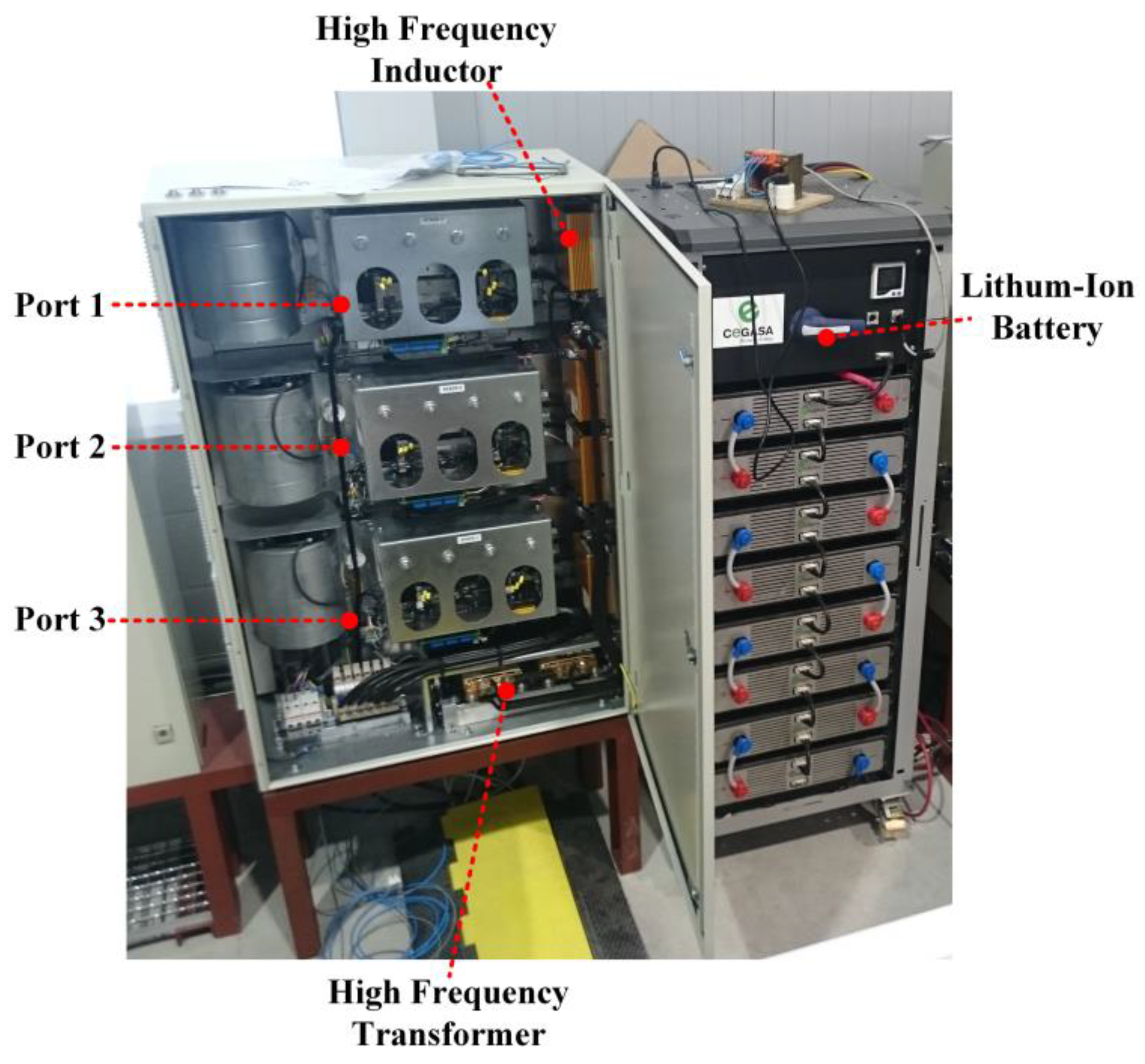
3.1. Converter Performance and Power Density Trade-Off

As the core component of a DC-based power system, the dual-active bridge (DAB) converter, as well as its 3-port triple-active bridge (TAB) converter version, were selected as another example. The under-considered TAB converter consists of three single-phase bridges and a multiwinding transformer as coupling component, where additional auxiliary inductors are used as power transfer components, as presented in Figure 8a. The mentioned converter was rated at 75 kW, with input voltage at 750 V and output voltage rated at 750 and 375 V, respectively. Because of the total power and voltage rating involved in this converter, the 62 mm power module for both SiC MOSFETs and Si IGBTs was considered, where both modules had a voltage rating of 1.2 kV and a current rating of 120A (at 125 °C). On the other hand, as mentioned earlier, the drop-in solution is often desired for SiC MOSFETs to replace Si IGBTs, where additional system-level adjustments can be eliminated, as illustrated in Figure 8b. It has been demonstrated that, because of the application of SiC MOSFETs, the efficiency of the TAB converter could be increased by approximately 2% when operating at full-load conditions at 20 kHz, which yielded losses of around 1500 W for the devices. The reduced device losses were considered to be the contribution of both the better conduction characteristics and the switching performance of SiC MOSFETs [17].
In terms of the conduction characteristics, benefit from the eliminated forward-on voltage, and capability of synchronous rectification of SiC MOSFETs, the conduction loss can be reduced for both forward conduction and reverse conduction conditions. In addition, because of the nature of DAB and TAB topology, soft-switching (zero-voltage switching off) can be achieved under certain load conditions. It should be noted that the soft-switching of this topology is achieved by the resonance between the auxiliary inductor and parasitic capacitance of the power devices. Because the SiC MOSFETs chip is thinner compared to Si IGBTs in this case, the parasitic capacitance for SiC MOSFETs (~6.5 nF) is relatively larger than that for Si IGBTs (~4.7 nF) and yields a larger resonance period. The larger resonant time will limit the soft-switching range and will result in more losses at light-load conditions. However, it is interesting to see that, even if the resonant period is longer for SiC MOSFETs, the switching losses for SiC MOSFETs are still lower than Si IGBTs. This is due to the optimum switching time of SiC MOSFETs, where the switching losses for SiC MOSFETs is 230 W at full-load conditions and approximately 1100 W for Si counterparts.
The reduced device loss is believed to contribute to the reduced size of the cooling equipment. As illustrated in Figure 9, the calculated overall heat-sink volume in liters is shown for Si IGBTs (red solid line) and SiC MOSFETs (blue solid line), where the switching frequency was kept at 20 kHz for both devices, and the heat-sink temperature varied from 50 to 100 °C. It is clear that an 80% reduction in heat-sink volume was achieved as a result of the reduced device losses of SiC MOSFETs. Obviously, the heat-sink volume could be reduced by compromising the heat-sink temperature; however, one-fifth of the heat-sink volume for SiC MOSFETs compared to Si counterparts was introduced at 100 °C heat-sink temperature.
The above discussion shows the benefits of SiC MOSFETs in increasing the overall efficiency of the TAB converter compared to Si counterparts under the same switching frequency. But it is important to observe the impact of size and volume reduction on the magnetic components in the TAB converter within SiC MOSFETs at higher switching frequencies, without any penalty on the efficiency. An optimized, multiwinding transformer has been designed to meet the operation at 80 kHz of the SiC MOSFET-based TAB converter, as illustrated in Figure 10. The ferrite-based high-frequency transformer employs modular design concepts, where four modules are used to achieve the required power (designed to 100 kW). In addition, planar technology is also used to achieve better power density properties. However, it is important to mention that the high dv/dt of SiC MOSFETs could bring serious insulation problems. As shown in Figure 11, the x-axis is the maximum current that flows through the power devices, and the vertical axis stands for the analytical values of the dv/dt values. The values of dv/dt for SiC MOSFETs are approximately 3 times more than the Si IGBTs values at low-current conditions, and they are around two times more at full-load conditions. The additional dv/dt could bring more partial discharges, which will result in insulation aging and failure. An enhanced insulation material and insulation distance are used for the newly designed transformer to avoid these problems. As a comparison, the dimension information of the transformer designed for an Si counterpart with the same rating is listed in Table 1.
As can be seen from Table 1, both volume and mass for the new transformer were less than half of the old one, which is a direct result of the higher operating frequency. It is important to see that the power density of the transformer designed for SiC MOSFETs was twice more than the one for Si IGBTs.

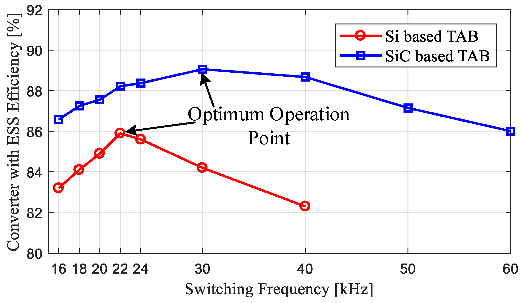
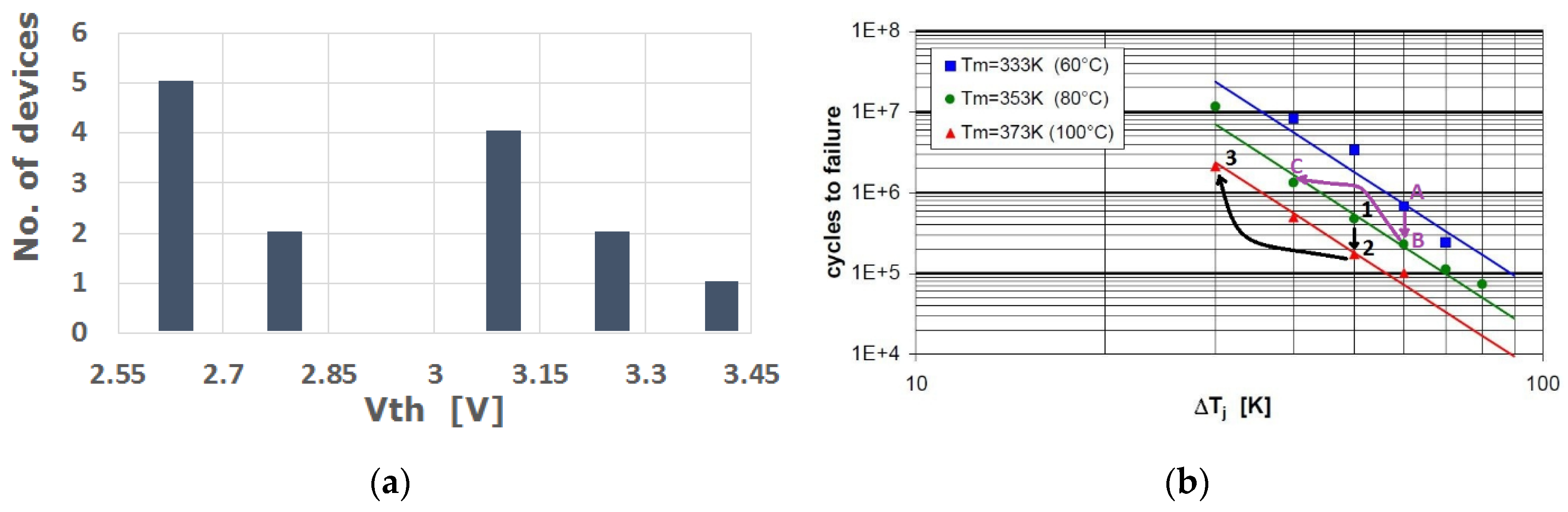
3.2. Impact of the Technology on Storage Device Utilization

In addition to the reduction on the magnetic components of the TAB converter, the higher switching frequency for SiC MOSFETs also boosted the performance of the attached lithium-ion battery. The experimental test rig for the TAB converter, with a lithium-ion battery as the energy storage element, is shown in Figure 12.
The measured efficiency values are reported in Figure 13 and Figure 14. In Figure 13, where the power is transferred from port 1 to port 2, the peak efficiency occurred at 20 kHz and 70 A by more than 98.5%. Moreover, the SiC MOSFET-based TAB converter showed efficient performance at 80 kHz, within the peak efficiency by approximately 97.5%. Figure 14 illustrates the efficiencies for both the SiC MOSFETs TAB converter and Si counterpart, where the power is transferred from port 3 to port 1. It should be noted that the lithium-ion battery was connected to port 3 and acted as the power supply for the converter. As can be seen, the efficiency increment was more than 2% and became larger at higher-frequency conditions. Because of the inductive behavior of the lithium-ion battery, the losses of the battery itself reduced with the increase of the switching frequency. It is interesting to see the reverse trend of the converter efficiency against battery efficiency, which resulted in the optimum operation point when taking the battery losses into consideration. As shown in Figure 15, the optimum operation point has been pushed from 22 to 30 kHz of the built TAB converter [18].

4. Discussion and Conclusions

The potential of WBG semiconductor technology as an enabler of incremental progress beyond state-of-the-art forms, in terms of the efficiency and power density of power converters used in renewable energy applications, has been amply demonstrated as a drop-in replacement for Si devices, that is, without the real need for custom design solutions. Minor adjustments at packaging and layout levels that target the minimization, next to parasitic inductance, also of parasitic common-mode capacitance, are an important first step towards exploiting its superior features and extracting all of the benefits that this technology can offer. It is anticipated that, at least in the midterm future, multilevel inverter topologies will play a key role in facilitating the large-scale deployment of WBG technology, especially in larger-power applications because of the high-temperature degradation of high-voltage (>3.3 kV) SiC MOSFETs on-state characteristics. Moreover, the bigger spread in the device’s electro-thermal parameters, as compared to Si, needs to be taken into account in the development of robust and reliable multichip power modules. For the sake of illustration, Figure 16a shows the measured threshold-voltage value on a sample population of 14 commercial devices all from the same manufacturing lot; the range is much broader than what is usual with Si transistors. Last but not least, heat-sink temperatures do not need to be drastically higher for significant advances in power density.
On a less positive note, as switching frequencies increase, low-load operation requires dedicated attention, careful consideration, and must be duly incorporated in the design optimization process. The most frequent or probable operational condition, not necessarily the full-load one, determines the actual energetic signature of the power converter, which is of great importance specifically in renewable energy systems. This particular aspect has already received attention in the specialist community, and first solutions have been put forward. However, it is still largely unexplored terrain, and there is still ample possibility to deliver important impacts, not only for renewable energies but also for avionics and transport applications in general, in which operation at about 25% of full-load is statistically the most frequent operational condition. Finally, though not explicitly addressed here, the topic of reliability still needs consideration. In particular, because of the equivalent semiconductor area reduction as compared to Si and because of the higher thermal conductivity of SiC over Si, much higher dynamic temperature excursions are expected during operation. This poses a problem for long-term technology validation and lifetime prediction based on standard accelerated reliability testing. In fact, as the amplitude of thermal cycles in real operation is increased, the acceleration margin that can be derived by Arrhenius law based types of testing, illustrated in Figure 16b, is significantly reduced, and, together with the identification of the most suitable constitutive materials to be used in SiC module development, it will represent a key challenge to reliable technology development for large-volume penetration. An aid to overcome this issue and deploy the technology while reliability is still discussed is to be found in the use of more advanced thermal management solutions, in particular, dynamic active cooling, with its demonstrated capability to reduce the amplitude of thermal cycles and the degradation level in power modules [19,20].

Author Contributions

A.C. co-funded and supervised the research activity; he co-authored the paper. E.G. was the researcher in charge of the PV inverter activities; he revised and co-edited the paper. A.S.H. was the researcher in charge of the wind inverter activities and characterization of the high-voltage (3.3 kV) MOSFETs. Z.W. was the researcher in charge of the SiC TAB characterization and testing; he co-wrote the paper. P.G.F. co-funded the activities on solid-state transformer and storage devices and supervised part of the testing and test setup; he revised and co-edited the paper.

Funding

This research received no external funding.

Conflicts of Interest

The authors declare no conflicts of interest.

References

  1. Kimoto, T.; Yamada, K.; Niwa, H.; Suda, J. Promise and Challenges of High-Voltage SiC Bipolar Power Devices. Energies 2016, 9, 908. [Google Scholar] [CrossRef]
  2. Gurpinar, E.; Castellazzi, A. Single-Phase T-Type Inverter Performance Benchmark Using Si IGBTs, SiC MOSFETs, and GaN HEMTs. IEEE Trans. Power Electron. 2016, 31, 7148–7160. [Google Scholar] [CrossRef]
  3. Barater, D.; Concari, C.; Buticchi, G.; Gurpinar, E.; De, D.; Castellazzi, A. Performance Evaluation of a Three-Level ANPC Photovoltaic Grid-Connected Inverter With 650-V SiC Devices and Optimized PWM. IEEE Trans. Ind. Appl. 2016, 52, 2475–2485. [Google Scholar] [CrossRef]
  4. Gurpinar, E.; Yang, Y.; Iannuzzo, F.; Castellazzi, A.; Blaabjerg, F. Reliability-Driven Assessment of GaN HEMTs and Si IGBTs in 3L-ANPC PV Inverters. IEEE J. Emerg. Sel. Top. Power Electron. 2016, 4, 965–969. [Google Scholar] [CrossRef]
  5. Gurpinar, E.; Castellazzi, A. Tradeoff Study of Heat Sink and Output Filter Volume in a GaN HEMT Based Single-Phase Inverter. IEEE Trans. Power Electron. 2017, 33, 5226–5239. [Google Scholar] [CrossRef]
  6. Hussein, A.; Castellazzi, A.; Wheeler, P.; Klumpner, C. Performance Benchmark of Si IGBTs vs. SiC MOSFETs in Small-Scale Wind Energy Conversion Systems. In Proceedings of the IEEE International Power Electronics and Motion Control Conference (PEMC), Varna, Bulgaria, 25–28 September 2016. [Google Scholar]
  7. Hussein, A.; Castellazzi, A. Optimization of Thermal Management and Power Density of Small-Scale wind Turbine Applications Using SiC-MOSFETs. In Proceedings of the IEEE 3rd International Future Energy Electronics Conference and ECCE Asia (IFEEC 2017–ECCE Asia), Kaohsiung, Taiwan, 3–7 June 2017. [Google Scholar]
  8. Hussein, A.; Castellazzi, A. Variable Frequency Control and Filter Design for Optimum Energy Extraction from a SiC Wind Inverter. In Proceedings of the International Power Electronics Conference (IPEC-Niigata 2018–ECCE Asia), Niigata, Japan, 20–24 May 2018. [Google Scholar]
  9. Castellazzi, A.; Fayyaz, A.; Gurpinar, E.; Hussein, A.; Li, J.; Mouawad, B. Multi-Chip SiC MOSFET Power Modules for Standard Manufacturing, Mounting and Cooling. In Proceedings of the International Power Electronics Conference (IPEC-Niigata 2018 -ECCE Asia), Niigata, Japan, 20–24 May 2018. [Google Scholar]
  10. Hussein, A.; Mouawad, B.; Castellazzi, A. Dynamic Performance Analysis of a 3.3 kV SiC MOSFET Half-Bridge Module with Parallel Chips and Body-Diode Freewheeling. In Proceedings of the IEEE 30th International Symposium on Power Semiconductor Devices and ICs (ISPSD), Chicago, IL, USA, 13–17 May 2018. [Google Scholar]
  11. Castellazzi, A.; Fayyaz, A.; Kraus, R. SiC MOSFET Device Parameter Spread and Ruggedness of Parallel Multichip Structures. Mater. Sci. Forum 2018, 924, 811–817. [Google Scholar] [CrossRef]
  12. Borghese, A.; Riccio, M.; Fayyaz, A.; Castellazzi, A.; Maresca, L.; Breglio, G.; Irace, A. Statistical Analysis of the Electrothermal Imbalances of Mismatched Parallel SiC Power MOSFETs. IEEE J. Emerg. Sel. Top. Power Electron. 2019, 7, 1527–1528. [Google Scholar] [CrossRef]
  13. Chowdhury, S.; Gurpinar, E.; Castellazzi, A. Full SiC Version of the EDA5 Inverter. In Proceedings of the IEEE 3rd Intern. Future Energy Electronics Conference and ECCE Asia (IFEEC2017-ECCE Asia), Kaohsiung, Taiwan, 3–7 June 2017. [Google Scholar]
  14. Hussein, A.; Castellazzi, A. Comprehensive Design Optimization of a Wind Power Converter Using SiC Technology. In Proceedings of the International Conference on Smart Grid (icSmartGrid), Nagasaki, Japan, 4–6 December 2018. [Google Scholar]
  15. Wang, Z.; Castellazzi, A.; Saeed, S.; Navarro-Rodríguez, Á.; Garcia-Fernandez, P. Impact of SiC Technology in a Three-Port Active Bridge Converter for Energy Storage Integrated Solid State Transformer Applications. In Proceedings of the IEEE 4th Workshop on Wide Bandgap Power DEVICES and Applications (WiPDA), Fayetteville, AR, USA, 7–9 November 2016. [Google Scholar]
  16. Wang, Z.; Castellazzi, A. SiC-based Triple Active Bridge Converter for Shipboard Micro-grid Applications with Efficient Energy Storag. In Proceedings of the International Conference on Smart Grid (icSmartGrid), Nagasaki, Japan, 4–6 December 2018. [Google Scholar]
  17. Wang, Z.; Castellazzi, A. Device Loss Model of a Fully SiC Based Dual Active Bridge Considering the effect of Synchronous Rectification and Deadtime. In Proceedings of the IEEE Southern Power Electronics Conference (SPEC), Puerto Varas, Chile, 4–7 December 2017. [Google Scholar]
  18. García, P.; Saeed, S.; Navarro-Rodríguez, Á.; Garcia, J.; Schneider, H. Switching Frequency Optimization for a Solid State Transformer With Energy Storage Capabilities. IEEE Trans. Ind. Appl. 2018, 54, 6223–6233. [Google Scholar] [CrossRef]
  19. Wang, X.; Castellazzi, A.; Zanchetta, P. Observer based temperature control for reduced thermal cycling in power electronic cooling. Appl. Therm. Eng. 2014, 64, 10–18. [Google Scholar] [CrossRef]
  20. Wang, X.; Wang, Y.; Castellazzi, A. Reduced Active and Passive Thermal Cycling Degradation by Dynamic Active Cooling of Power Modules. In Proceedings of the IEEE 27th International Symposium on Power Semiconductor Devices & IC’s (ISPSD), Hong Kong, China, 10–14 May 2015. [Google Scholar]
Figure 1. Quantified impact of higher fs capability of gallium nitride (GaN) on inverter power density improvement: (a) output filter design for 3 values of fs; (b) output inductor current and detail of current ripple, highlighting same operational conditions in the benchmark exercise.
Energies 12 04462 g001
Figure 2. Relation between filter and heat-sink volume as a function of fs, for a given target heat-sink temperature, THS: (a) target THS = 50 °C; (b) target THS = 80 °C.
Energies 12 04462 g002
Figure 3. Analytical study of required heat-sink thermal resistance and corresponding volume to keep a target maximum THS at full load operation (fully passive heat-sink is assumed). The power loss models were validated up to 125 °C.
Energies 12 04462 g003
Figure 4. Efficient and dense architecture (EDA5) hybrid multilevel full SiC inverter architecture: (a) topology circuit schematic; (b) 15 kW hardware prototype (top) and output voltage and current waveforms (bottom).
Energies 12 04462 g004
Figure 5. Output characteristics of recent technology, 3.3 kV MOSFET, and body-diode measured at two different temperature values: (a) MOSFET; (b) body-diode.
Energies 12 04462 g005
Figure 6. Measured inverter efficiency as a function of output power for various fs values.
Energies 12 04462 g006
Figure 7. (a) Wind speed distribution and power output of a 12.5 kW-rated residential wind turbine; (b) energy lost in one year for the various speed–output power values and three different fs values.
Energies 12 04462 g007
Figure 8. Triple-active bridge (TAB) converter, (a) topology circuit schematic; (b) under-considered SiC MOSFETs (left-hand side) and Si IGBTs (right-hand side).
Energies 12 04462 g008
Figure 9. Analytical study of the heat-sink volume for both the SiC MOSFET-based TAB converter and Si counterpart, with varied maximum heat-sink temperature.
Energies 12 04462 g009
Figure 10. Optimized multiwinding high-frequency transformer for the SiC MOSFET-based TAB converter: (a) whole multicore transformer; (b) detail of individual core.
Energies 12 04462 g010
Figure 11. Analysis of the dv/dt for both SiC MOSFETs and Si IGBTs under varied peak device currents, for the TAB converter.
Energies 12 04462 g011
Figure 12. Hardware prototype of the triple-active bridge converter, rated at 75 kW, with a connected lithium-ion battery.
Energies 12 04462 g012
Figure 13. Efficiency measurements of the SiC MOSFET-based TAB converter with power transferred from port 1 to port 2; (a) efficiency performance with varied load conditions; (b) switching performance with varied switching frequency conditions.
Energies 12 04462 g013
Figure 14. Efficiency measurements of the SiC MOSFET-based TAB converter with power transferred from port 3 to port 1; (a) converter-only efficiency measurement; (b) calculated normalized battery losses.
Energies 12 04462 g014
Figure 15. Converter with battery efficiency showing optimum operation points.
Energies 12 04462 g015
Figure 16. (a) Measured SiC MOSFET spread in threshold voltage (Vth) value for a sample population of 14 commercial devices from the same manufacturing lot; (b) experimental lifetime validation procedure demonstrating the applicability of a Coffin–Manson-type model over the considered temperature range.
Energies 12 04462 g016
Table 1. Size information for the designed transformer.
OldNew
Dimensions (mm)375 × 327 × 73280 × 200 × 75
Volume (L)8.9524.2
Mass (kg)22.610.8
Power Density (kW/L)11.1723.8

