1. Introduction
Efficient heat removal is an increasingly important consideration within modern microelectronics. The current trend of 3D packaging and GaN-based high power devices will only exacerbate the demands on thermal management [
1]. A significant source of thermal resistance within electronics packages is at the interface between mating surfaces. Thermal interface materials (TIMs) are used to reduce this resistance, by filling out voids and increasing the real contact area between the surfaces [
2]. TIMs should preferably have high thermal conductivity, perfect contact with both surfaces, no thermal contact resistance, and should also be able to absorb stresses in the interface, e.g., due to coefficient of thermal expansion (CTE) mismatch. Today, commercially used TIM can be roughly divided into polymer-based TIMs filled with thermally conductive particles, and solder-based TIMs. However, polymer-based TIMs are limited in thermal conductivity, and despite large research effort into novel fillers, the gains remain limited [
3]. On the other hand, solder-based TIMs have excellent thermal performance, but have other limitations such as reliability issues at low bond lines.
As an alternative to existing TIM concepts, novel TIMs based on low-dimensional carbon allotropes such as graphene and carbon nanotubes (CNTs) have gained interest recently owing to their excellent thermal conductivity, of up to 6000 and 3000 W/mK for graphene [
4] and CNTs, respectively [
5]. While 2D graphene allows for excellent in-plane thermal conductivity suitable for heat spreading, arrays of vertically aligned CNTs instead allows for highly anisotropic through-plane thermal transport due to their 1D geometry. In addition, CNTs are flexible [
6], and a CNT array can conform to the mating TIM surfaces, and each CNT can span the entire interface in a TIM application. This eliminates internal thermal contact resistances, making CNT arrays a highly attractive option for TIMs. The effective thermal conductivity of CNT arrays is proportional to the CNT packing density, which is typically less than 10% [
7]. Previous studies have experimentally found CNT arrays with an effective thermal conductivity of up to 270 W/mK [
7], although more typical values are an order of magnitude lower [
8]. Despite this, CNT array TIMs have been shown to achieve performance on par with the best solder-based TIM [
3].
CNT arrays are synthesized using chemical vapor deposition (CVD), usually on Si substrates. To utilize them in a TIM application, the most basic approach is the dry contact method, in which the as-grown CNT array is pressed against an opposing surface with a constant force applied in order to force the CNT array to conform to the surface [
9,
10]. By varying CNT growth parameters and applied pressure, the thermal performance can be optimized and tailored towards specific applications. However, uneven CNT lengths prevent every CNT to achieve contact with the opposing substrate even at high pressures. Since the inter-CNT heat transfer is very low, only CNTs in contact with both surfaces contribute to the total heat transfer, severely limiting the performance.
To increase the fraction of CNTs in contact, a bonding agent that partially penetrates the array can be used. Solder is one such possible agent, where the CNT array is pressed against a reflowed metal layer, partially embedding the CNT tips into the metal phase. This results in a TIM with reduced thermal interface resistance and which does not require applied pressure after reflow. However, the thermal contact resistance between CNTs and metal has been shown to be relatively high [
11], thus, to reduce the thermal interface resistance further, organic functionalization can be used [
12,
13]. Organic functionalization of CNT arrays using polymers acts similarly to metal bonding, but can utilize covalent bonds to contact the CNT tips. As the thermal transport in CNTs is largely phononic in nature [
11], organic molecules has a much smaller boundary resistance at the tips, and should therefore be suitable for high-performing CNT array TIMs.
The vertical alignment of the CNT array allows for individual CNTs to strain independently in the
x-y plane. Together with the flexible nature of CNTs [
14], a CNT array could mechanically decouple the two joined surfaces in a TIM application. This decoupling could potentially act as a buffer that could absorb stress originating from mismatches of the coefficient of thermal expansion (CTE) between different materials within the electronics system and thereby increase the performance and reliability. However, to date, there has, to the authors’ knowledge, been no studies on the reliability of CNT TIMs, which could confirm this potential.
In this study, we subjected fabricated CNT array TIMs to thermal cycling and subsequently measured the thermal performance to investigate the degradation of the TIM. This paper is an extended and revised version of a conference report that was presented at Therminic 2018 [
15] and follows the work of Ni et al. [
16] and Daon et al. [
17] on the HLK5 polymer used to bond CNT arrays for TIM applications. This is the first reported study on the thermal reliability of a CNT array TIM. As CNT technology has matured, including large scale fabrication of CNT arrays [
18], ensuring the reliability of fabricated TIM remains an important step towards market realization.
2. Materials and Methods
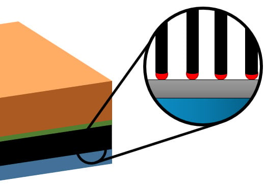
The TIM setup in this study consistrf of a CVD grown CNT array on a Si substrate, bonded through a polymer layer to a Cu superstrate acting as a heat sink. The assembled structure can be seen in
Figure 1.
The CNT arrays were synthesized on square Si substrates, 280
m thick and 10 mm on the side. The catalyst structure consisted of a 10 nm thick Al
O
diffusion barrier layer and a 1 nm thick Fe catalyst layer deposited using e-beam evaporation. The CNT synthesis was performed in a commercial Aixtron Black Magic II cold-wall CVD reactor. The substrates were placed on a graphite heater inside a vacuum chamber, and annealed at 500
C under a flow of 837 sccm of H
gas for 3 min. During the growth phase, 200 sccm of C
H
was also introduced into the chamber while the temperature was ramped up to 700
C. This step was held for 20 s, which yielded a CNT array of 15
m. The growth was terminated by shutting off the heater and flushing the chamber with N
. This CVD process resulted in vertically aligned CNTs, with the iron catalyst particles at the roots of each CNT, as shown in the inset of
Figure 1. The orientation and uniformity of the CNT array was verified by scanning electron microscope (SEM), and the resulting images can be seen in
Figure 2. A more detailed description of the CVD process can be found in Reference [
19].
The grown CNT arrays were subsequently bonded to 10 mm by 10 mm, 2 mm thick Cu pieces using a previously described bonding process [
17]. The polymer functionalization was spin coated onto the Cu pieces, and then the CNT array was pressed into the polymer layer. The same process time, temperature and pressure were used for all samples.
The reliability of the CNT array TIMs was investigated by subjecting the assembled interface to thermal cycling. The thermal cycling test condition “B” from the JEDEC standard [
20] was chosen, corresponding to a cycling between −55
C and 125
C, with a ramp time of 10 min and holding time at each extreme for 20 min. The cycle time for each cycle was 60 min, and the investigation ran for 500 cycles, with thermal measurements every 100 cycles.
The total thermal interface resistance of the CNT array TIM was measured before and during thermal cycling using the laser flash method. A laser pulse induced a heat impulse on one side of the assembled sandwich structure and the transient temperature response on the other side was monitored using an IR detector. By fitting material parameters of the Cu and Si pieces, the remaining thermal interface resistance could be extracted, using a two layer plus contact resistance model [
21]. The contact resistance in the model corresponded to the total thermal interface resistance R
, as shown in
Figure 3. R
in turn included contribution from the effective bulk thermal conductivity of the CNT array
, the thermal boundary resistances R
and R
at both the CNT/Si and CNT/Cu interfaces, and the bond line thickness (BLT) of the TIM.
To investigate the individual contributions of the thermal resistance components in
Figure 3, we used the PPR method on as-grown CNT array samples. In the PPR method that is illustrated in
Figure 4A, a picosecond Nd:YAG pump beam laser pulse was used to heat the temperature of the sample, while a He-Ne probe beam laser monitored the transient temperature dependent reflectivity response of the sample surface. The temperature response could be modeled as a one-dimensional heat conduction problem, and by fitting the model to the experimental temperature response the thermal conductivity of up to three different layers, together with the thermal boundary resistance between them, could be extracted. For the method to work, the top layer needed to have a temperature dependent reflectivity, thus 300 nm TiN was sputtered onto the CNT array, as shown in
Figure 4B. The PPR measurement setup is described in more detail in References [
22,
23,
24]. The PPR measurement could determine the thermal resistance components from the bulk CNT array and the Si/CNT thermal boundary resistance R
, which combined with R
from the laser flash measurements allowed for the extraction of the CNT/Cu boundary resistance R
as well.
To investigate the chemical evolution of the Si/CNT interface during thermal cycling, we used a PHI 5000C X-ray photoelectron spectroscopy (XPS) system to analyze samples before and after thermal cycling. By analyzing the elemental composition at the delaminated interface of the CNT array TIM, information about the interface degradation could be obtained. We analyzed both the CNT roots on the Cu superstrate from the delaminated samples, as well as the silicon substrate before and after thermal cycling. The acquired spectra was shifted to coincide with the 284.8 eV C1s peak and adjusted after a Shirley type background prior to peak fitting.
3. Results and Discussion
The thermal performance of the fabricated CNT array TIM interfaces was investigated using the laser flash and PPR methods. Different sets of samples were prepared for each method, with CNT array TIMs illustrated in
Figure 1 intended for laser flash measurements and TiN coated CNT arrays in
Figure 4B for PPR measurements. Both sets of samples were measured before and after thermal cycling to investigate how CNT array TIMs age during usage.
The laser flash measurements were first conducted on CNT array TIMs before cycling and then at every consecutive 100th cycle up to the completed 500 cycles. Thermal interface resistance results calculated after measurement for samples before and during cycling are presented in
Figure 5A,B, respectively. Before thermal cycling, the CNT array TIMs had an average thermal interface resistance of of 1.7 mm
K/W ± 0.28 at 20
C.
The thermal aging behavior of the CNT array TIM is shown in
Figure 5B. Already at 100 thermal cycles, the thermal interface resistance increased 20 times from 1.7 mm
K/W to 34.7 mm
K/W. Subsequent thermal cycling further increased the thermal resistance from 100 to 500 cycles, although at a slower rate. After 500 cycles, the R
increased to 46 mm
K/W.
It should be noted that some of the measured samples exhibited an even sharper increase in terms of thermal interface resistance during the cycling. However, these samples delaminated by themselves before the thermal cycling could be completed and were for that reason disregarded. All of the samples were delaminated by shearing, which showed that all samples, before and after thermal cycling, detached on the Si/CNT side of the interface leaving all the CNTs on the Cu superstrate side, as shown in
Figure 6.
The increased thermal interface resistance shown in
Figure 5B was determined to originate from either the CNT array or from the thermal contact on either the Si substrate side or on the Cu superstrate side. The CNTs themselves were considered to be thermally stable at the temperature range of the cycling and the effective thermal conductivity
of the CNT array should therefore remain constant [
25]. Furthermore, the polymer functionalization did not show any signs of deterioration during this study as the Si/CNT interface seemed to fail before any noticeable effects on the CNT/polymer adhesion could be distinguished. This leaves the probable failure of the CNT array TIMs to a degradation of the contact between the CNT and the Si substrate that would result in a similar increase of the thermal contact resistance R
. This could originate either from a CTE mismatch between the Cu superstrate and the Si substrate that would result in an uprooting of the CNTs or a chemical degradation of the contact point where the CNT was attached to the Si substrate.
To further investigate the degradation of the CNT/catalyst attachment, TiN covered CNT array samples, as presented in
Figure 4B, were evaluated using PPR before and after thermal aging. These samples were free standing arrays on a silicon substrate, thus no CTE mismatch would degrade the structure during cycling, which leaves only the Si/CNT contact to affect the thermal performance. The samples were cycled 30 times, as the main degradation of the CNT array TIM was found to occur during the first 100 cycles. The attained temperature response curves were fitted to a numerical model of the sample stack to obtain the thermal conductivity
of the CNT array as well as the thermal boundary resistance R
between the CNT and Si chip.
Figure 7 shows the measured temperature response from the PPR measurements. Before thermal cycling, an effective thermal conductivity (
) of 71 W/mK and a thermal boundary resistance (R
) of 0.96 mm
K/W were found. Together with the R
value obtained from the laser flash measurement presented in
Figure 5A, R
could be calculated using the thermal interface relation stated in
Figure 3. This relation gave a R
of 0.49 mm
K/W for the CNT array TIMs. By comparison, this means that the polymer functionalization was about twice as good as the Si/CNT boundary on the other side of the interface in terms of thermal boundary resistance.
After subjecting the TiN covered CNT arrays to 30 cycles of thermal cycling, R
increased with 137%, which could be found from the slower temperature decrease of the aged CNTs in
Figure 7. While this is a significant degradation, it is not enough to explain the increase of the total thermal interface resistance, as shown in
Figure 5B. The remaining increase could be attributed to uprooting of the CNT array due to a combination of CTE mismatch induced stress and chemical degradation of the interface.
To further investigate the degradation of the Si/CNT interface, the elemental composition of the delaminated interfaces was investigated using XPS analysis. According to the illustration in
Figure 1, the Si/CNT interface was composed of the Si substrate, the Al
O
barrier layer, Fe catalyst nanoparticles as well as the CNT. The XPS analysis showed no Al signal on the CNT roots on the Cu superstrate after delamination, which indicates that the failure occurred in the Fe interface between the CNTs and the Al
O
layer. The Fe peak from the XPS measurements is shown in
Figure 8 for both the CNT roots (
Figure 8A) and Si chip (
Figure 8B). The Fe traces found shown in
Figure 8A could be identified from the Fe2p
peak at 709.5 eV as well as Fe2p
peak at 723.5 eV, both of which related to iron oxide species [
26]. Comparing the average signal found on samples before and after shearing, it was found that traces in the cycled samples were 70% lower than those in the samples that were sheared without thermal cycling. According to these results, the CNT were uprooted together with the Fe catalyst nanoparticle during shearing. After thermal cycling, the bond between the CNT and the Fe catalyst nanoparticle had weakened, thereby leaving the Fe particles on the Si substrate.
The silicon substrates from the TiN covered samples before and after aging were also analyzed using XPS, as shown in
Figure 8B. The CNT arrays were removed from the silicon substrate using a tape to reveal the Fe catalyst layer underneath. In both cases, peaks could be identified related to the metallic Fe2p
at 706.6 eV, oxide Fe2p
at 710 eV, satellite Fe2p
peak at 719 eV as well as the oxide Fe2p
peak at 723.5 eV [
27]. After aging, the metallic Fe2p
had decreased in intensity by 15% in comparison to the oxide Fe2p
and Fe2p
peaks, which indicates that the catalyst layer on the Si substrate had gone through a noticeable oxidation already after 30 thermal cycles. However, additional studies will be required to conclude if this oxidation process directly responsible for the delamination issues found in the CNT array TIM.
Regardless of the cause for delamination, it was obvious that the bonded surface at the CNT tips was stronger than the Si/CNT substrate. This indicates that a process to transfer the array from the growth substrate may result in a more reliable interface. Such an approach, where both the CNT tips and roots would be bonded to a surface, has been demonstrated in several publications [
28,
29]. This approach would also have the benefit of bypassing the challenge of making the CNT CVD synthesis CMOS compatible, since the CVD process normally requires significantly higher temperatures than the CMOS processes allow [
30].
4. Conclusions
In this study, we investigated the thermal cycling behavior of a CNT array TIM sandwiched between a Si growth substrate and a polymer bonded Cu superstrate. The results obtained show that the CNT array TIM is susceptible to degradation after thermal aging. While the TIMs fabricated in this study are on par with similar state-of-the-art TIMs presented previously, laser flash measurements show an increase in thermal interface resistance of 20 times within the first 100 cycles, and a delamination at the Si/CNT interface. In addition to delamination, PPR measurements reveal that the polymer bonded interface has a factor of two lower thermal boundary resistance than the growth interface, which indicates that the Si/CNT interface needs further improvement in order for CNT array TIMs to be viable.
A combination of PPR and XPS measurements further revealed a degradation of the Si/CNT interface. PPR measurements revealed a 137% increase in thermal boundary resistance after 30 cycles. XPS analysis of the uprooted CNTs showed a decrease in iron on the CNT roots after thermal cycling, indicating a weakening of the CNT-Fe bond during thermal cycling. Further analysis on the Si substrate showed oxidation of the Fe catalyst, which may contribute to the weakening of the bond.
While this study revealed a weakening of the Si/CNT bond during thermal cycling, even without CTE mismatch induced stress, CTE mismatch was most likely still a significant contributor to the interface failure, and a more thorough investigation on this effect was required. Nonetheless, even systems without significant CTE mismatch may experience degradation, and transfer and bonding towards both mating TIM surfaces may be required to create a reliable interface.

 ,
, 


