Article

A Duty Cycle Space Vector Modulation Strategy for a Three-to-Five Phase Direct Matrix Converter

1
School of Electrical Engineering, Northeast Electric Power University, Jilin 132012, China
2
Jilin Electric Power Survey Design Limited Company, Jilin 132000, China
*
Author to whom correspondence should be addressed.
Energies 2018, 11(2), 370; https://doi.org/10.3390/en11020370
Submission received: 18 January 2018 / Revised: 30 January 2018 / Accepted: 31 January 2018 / Published: 5 February 2018

Abstract

:
The duty cycle space vector (DCSV) modulation strategy is of universal significance, and the method can be utilized for different modulation approaches. In this paper, the vectors of input voltages and currents are equivalently represented by a complex two-dimensional space vector, and the vectors of output voltages and currents are equivalently represented by two two-dimensional space vectors. Then, input–output relationships in both the d1-q1 space and the d3-q3 space are obtained. Because the desired output voltages are only mapped onto a reference voltage space vector in the d1-q1 space, the reference in the d3-q3 space is regarded as zero, in order to reduce harmonics of output voltages to the greatest extent. Then, the duty cycle space vector modulation strategy of the three-to-five phase direct matrix converter (DMC) is deduced. Considering the influence of the zero vector on system performance, the duty cycles are decomposed and recomposed to obtain the space vector pulse width modulation (SVPWM) strategy based on the duty cycle space vector. Finally, the accuracy and feasibility of the theory are verified through experiments.

1. Introduction

Multiphase drive systems involving more than three phases have been receiving increasing attention because of their inherent advantages over the traditional three-phase motor drives. They reduce the amplitude and increase the frequency of torque pulsations, reduce the rotor harmonic current losses, reduce the current per phase without increasing the voltage per phase, and lower the DC link current harmonics [1,2,3,4]. Therefore, it is necessary to develop multiphase power electronic converters to supply such multiphase systems. Consequently, the multiphase matrix converter (MC) has been widely studied and used in many different applications such as wind energy conversion systems, diesel generators, microturbines, electric aircraft, and ship propulsion [5,6,7,8,9,10].
The three-to-five phase direct matrix converter is a typical multiphase power converter, and its topology is shown in Figure 1. It has become a focus of research in the field of power transmission and conversion due to its excellent performance. The advantages of DMCs include their sinusoidal input and output currents, simple and compact power circuits due to the lack of electrolytic capacitors, bidirectional power flow, and controllable input power factors [11,12]. However, modulation strategies become more complex due to the increasing number of output phases.
Recently, many modulation strategies for the multiphase MC have been developed, including direct duty ratio pulse width modulation (DPWM), space vector pulse width modulation, and carrier-based pulse width modulation (CBPWM) [13,14,15,16,17]. The pulse width modulation (PWM) technique is presented in [13] for a generalized three-to-k phase MC topology based on direct duty ratio control. SVPWM is discussed in [14] for a three-to-five phase MC considering only outer large length space vectors. However, for SVPWM implementation, only 93 vectors (90 active and 3 zero vectors) can be used, and the complete space vector model of three-to-five phase MC topology is presented in [15]. To simplify the SVPWM, the CBPWM method has been adopted by researchers. The CBPWM technique is proposed in [16] to achieve the maximum voltage transfer ratio (VTR) in the linear and over-modulation modes. A novel method of CBPWM based on space vector modulation analysis is presented in [17], using only one symmetrical triangular carrier signal to generate the PWM signals for all of the switches. Obviously, the performance of DMC is highly dependent on the control algorithms.
In this paper, a new generalized strategy—duty cycle space vector modulation—is proposed to control the three-to-five phase DMC. According to this strategy, the duty cycles have been deduced and the general expression of them has been obtained. In addition, the proposed strategy is a general solution to the modulation problem of the three-to-five phase DMC. In addition, this modulation strategy can be easily applied to multiphase DMCs in the future. Then, the previously proposed modulation (DPWM, SVPWM, CBPWM) strategies are considered as a particular case of the DCSV. In this paper, the SVPWM based on DCSV is obtained by decomposing and recombining the duty cycles of 15 switches. Finally, in order to show the validity of the proposed DCSV strategy, an experimental platform is established.

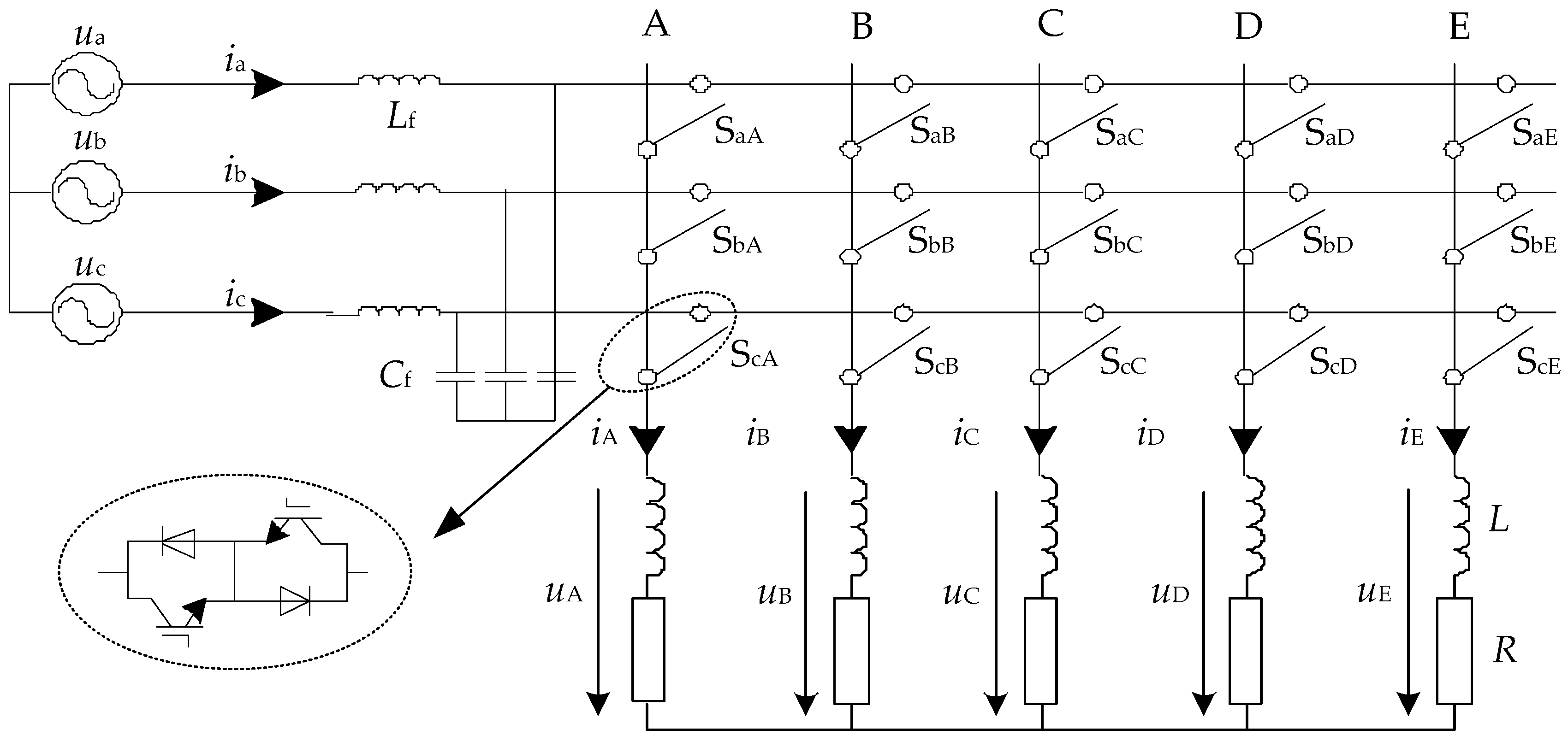
2. Modeling of the Three-to-Five Phase DMC

The topology of the three-to-five phase DMC is shown in Figure 1. Fifteen bidirectional switches (BDSs) are used to connect five output phases to three input phases, and they are defined as SxX (the subscripts of x and X are employed to describe the inputs and outputs, respectively), where x ∈ {a, b, c}, X ∈ {A, B, C, D, E}; ua, ub, uc and ia, ib, ic are three-phase input voltages and currents, respectively, and uA, uB, uC, uD, uE and iA, iB, iC, iD, iE are five-phase output voltages and currents, respectively. Lf and Cf are the inductor and capacitor of the input filter, respectively, which smooth the current waveform.
The output voltages and input currents of the three-to-five phase DMC are expressed respectively as the following forms:
( u A u B u C u D u E ) = ( d aA d bA d cA d aB d bB d cB d aC d bC d cC d aD d bD d cD d aE d bE d cE ) ( u a u b u c ) = D ( u a u b u c )
( i a i b i c ) = ( d aA d bA d cA d aB d bB d cB d aC d bC d cC d aD d bD d cD d aE d bE d cE ) T ( i A i B i C i D i E ) = D T ( i A i B i C i D i E )
where T represents transposition; the variables dxX (x ∈ {a, b, c}, X ∈ {A, B, C, D, E}) are duty cycles of SxX; and D is the modulation matrix.
In order to avoid short circuits on the input side and open circuits on the output side, only one switch in every output phase is kept in the ON state at any time. Thus, the constraints of the duty cycles are expressed as daX + dbX + dcX = 1.

3. Space Vector Expression of the Three-to-Five Phase DMC

3.1. Space Vector of the Input Side

In the three-phase symmetric system, except for the (6n ± 3)th harmonics corresponding to zero sequence components, all the (6n ± 1)th harmonics of three-phase variables are equivalently represented by a two-dimensional complex space vector [18]. Thus, the space vector of the input side of the three-to-five phase DMC can be represented as follows:
U i = 2 3 ( u a + u b e j 2 3 π + u c e j 4 3 π )
I i = 2 3 ( i a + i b e j 2 3 π + i c e j 4 3 π )
where Ui is the space vector of input voltages, and Ii is the space vector of input currents.

3.2. Space Vector of the Output Side

Similarly, the concept of the space vector can be extended to the five-phase symmetric system. Each five-dimensional variable has four freedom degrees (except zero sequence components), and can be mapped to two spaces (d1-q1 space and d3-q3 space) according to Park’s transformation of the five-dimensional space vector. Therefore, two orthogonal space vectors synchronously rotating in the d1-q1 and d3-q3 spaces can equivalently express five-phase variables except for the zero sequence components. All the (10n ± 1)th harmonics of five-phase variables can be equivalently expressed as AC components with the frequency of (10n ± 1)ω in the stationary d1-q1 space, whereas the (10n ± 3)th harmonics of five-phase variables can be equivalently expressed as AC components with the frequency of (10n ± 3)ω in the stationary d3-q3 space [19]. Thus, the space vectors of the output side of the three-to-five phase DMC can be represented as follows:
U o 1 = 2 5 ( u A + u B e j 2 5 π + u C e j 4 5 π + u D e j 6 5 π + u E e j 8 5 π )
I o 1 = 2 5 ( i A + i B e j 2 5 π + i C e j 4 5 π + i D e j 6 5 π + i E e j 8 5 π )
U o 3 = 2 5 ( u A + u B e j 6 5 π + u C e j 2 5 π + u D e j 8 5 π + u E e j 4 5 π )
I o 3   = 2 5 ( i A + i B e j 6 5 π + i C e j 2 5 π + i D e j 8 5 π + i E e j 4 5 π )
where Uo1 and Io1 are the space vectors of the output voltages and currents in the d1-q1 space, respectively; and Uo3 and Io3 are in the d3-q3 space.

4. Duty Cycle Space Vector Approach

4.1. Single-Phase Duty Cycle Space Vector

The duty cycle space vector of an arbitrary output phase is defined in [20], and is expressed as follows:
D X = 2 3 ( d a X + d b X e j 2 3 π + d c X e j 4 3 π )
Due to the constraint daX + dbX + dcX = 1, the expression of each duty cycle can be derived as follows:
d x X = 1 3 + D X e j ( k 1 ) 2 3 π
where x = a, b, c; k = 1, 2, 3.

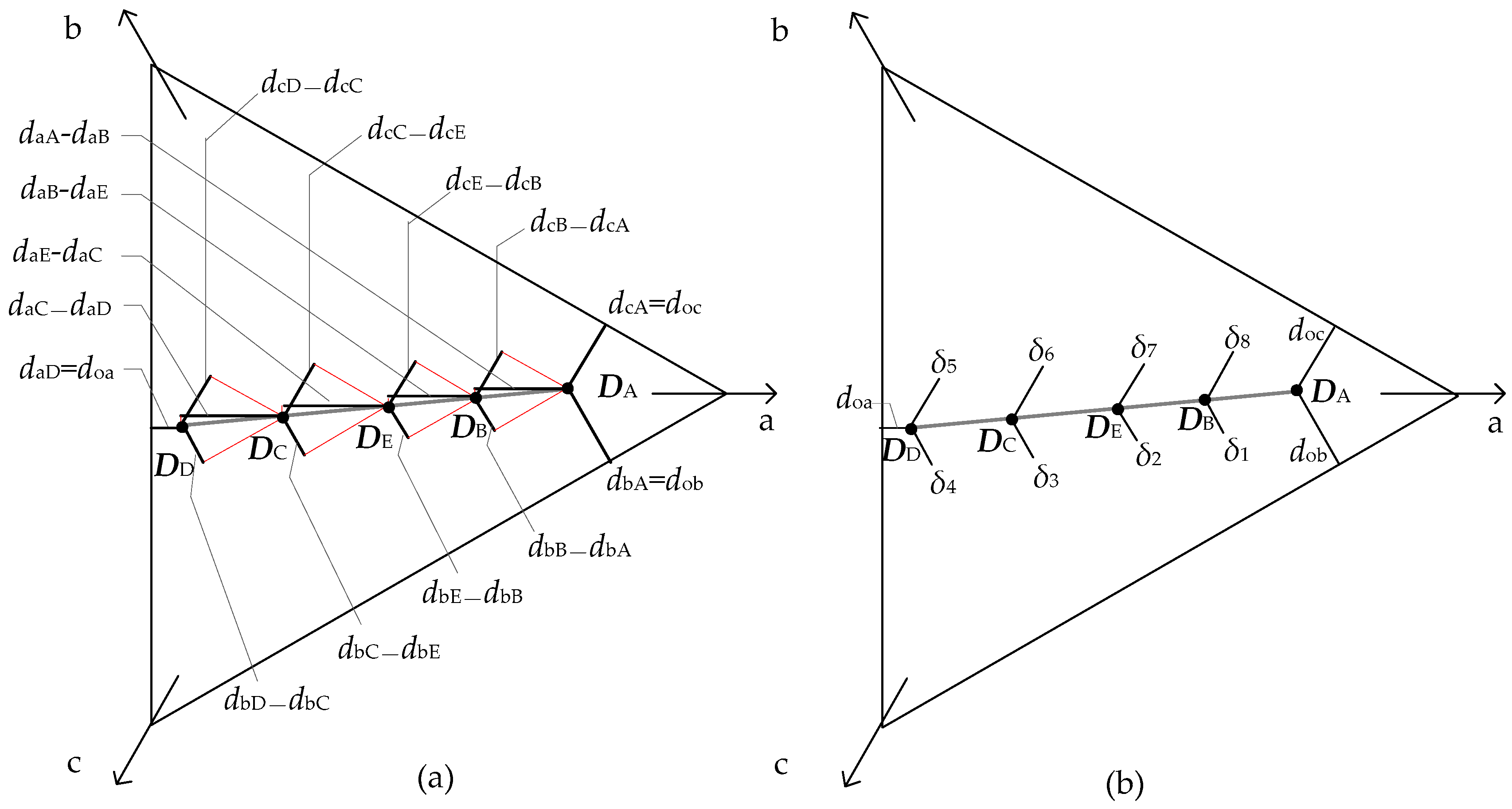
4.2. Five-Phase Duty Cycle Space Vector

The duty cycle space vector DX, instead of the modulation matrix D, can be used to express the relationships of output voltages and input currents. Then, Equations (1) and (2) can be rewritten in the d1-q1 space as follows:
U o 1 = 3 10 U i ( D A * + D B * e j 2 5 π + D C * e j 4 5 π + D D * e j 6 5 π + D E * e j 8 5 π ) + 3 10 U i * ( D A + D B e j 2 5 π + D C e j 4 5 π + D D e j 6 5 π + D E e j 8 5 π )
I i 1 = 1 2 I o ( D A + D B e j 8 5 π + D C e j 6 5 π + D D e j 4 5 π + D E e j 2 5 π )   + 1 2 I o * ( D A + D B e j 2 5 π + D C e j 4 5 π + D D e j 6 5 π + D E e j 8 5 π )
Likewise, the input–output relationships in the d3-q3 space can be rewritten as follows:
U o 3 = 3 10 U i ( D A * + D B * e j 6 5 π + D C * e j 2 5 π + D D * e j 8 5 π + D E * e j 4 5 π ) + 3 10 U i * ( D A + D B e j 6 5 π + D C e j 2 5 π + D D e j 8 5 π + D E e j 4 5 π )
I i 3 = 1 2 I o ( D A + D B e j 4 5 π + D C e j 8 5 π + D D e j 2 5 π + D E e j 6 5 π ) + 1 2 I o * ( D A + D B e j 6 5 π + D C e j 2 5 π + D D e j 8 5 π + D E e j 4 5 π )
Five new variables—D1, D2, D3, D4, and D0—as defined by the Equations (11)–(14), can be defined as follows:
D 1 = 1 5 ( D A + D B e j 2 5 π + D C e j 4 5 π + D D e j 6 5 π + D E e j 8 5 π ) D 2 = 1 5 ( D A + D B e j 4 5 π + D C e j 8 5 π + D D e j 2 5 π + D E e j 6 5 π ) D 3 = 1 5 ( D A + D B e j 6 5 π + D C e j 2 5 π + D D e j 8 5 π + D E e j 4 5 π ) D 4 = 1 5 ( D A + D B e j 8 5 π + D C e j 6 5 π + D D e j 4 5 π + D E e j 2 5 π ) D 0 = 1 5 ( D A + D B + D C + D D + D E ) .
The inverse transformation expressions of Equation (15) are
D A = D 1 + D 2 + D 3 + D 4 + D 0 D B = D 1 e j 8 5 π + D 2 e j 6 5 π + D 3 e j 4 5 π + D 4 e j 2 5 π + D 0 D C = D 1 e j 6 5 π + D 2 e j 2 5 π + D 3 e j 8 5 π + D 4 e j 4 5 π + D 0 D D = D 1 e j 4 5 π + D 2 e j 8 5 π + D 3 e j 2 5 π + D 4 e j 6 5 π + D 0 D E = D 1 e j 2 5 π + D 2 e j 4 5 π + D 3 e j 6 5 π + D 4 e j 8 5 π + D 0 .
Then, the following equations can be obtained by substituting Equation (16) into Equations (11) and (12):
U o 1 = 3 2 U i D 4 * + 3 2 U i * D 1 I i 1   = 5 2 I o D 4 + 5 2 I o * D 1 .
Equation (17) shows the input–output relationship of the three-to-five phase DMC effectively and compactly. In order to obtain the desired input power factor, suppose that ψ ¯ is the desired phase angle for the input current space vector. Then, Equation (17) can be rewritten in the following form:
U o 1 = 3 2 U i D 4 * + 3 2 U i D 1 ( I o D 4 + I o * D 1 ) j ψ ¯ = 0 .
The general solution of Equation (18), which is valid for any value of the parameter λ1, is
D 1 = U o 1 ψ ¯ 3 ( U i ψ ¯ ) + λ 1 U i * I o * D 4 = U o 1 * ψ ¯ 3 ( U i ψ ¯ ) λ 1 U i * I o .
Similarly, from substituting Equation (16) into Equations (13) and (14), D2 and D3 also can be deduced as follows:
D 3 = U o 3 ψ ¯ 3 ( U i ψ ¯ ) + λ 2 U i I o D 2 = U o 3 ψ ¯ 3 ( U i ψ ¯ ) λ 2 U i I o .
In Equations (19) and (20), λ1 and λ2 are the degrees of freedom, which can be utilized only if the phase angle of the output current is known. In practical applications, the method of selecting λ1 = λ2 = 0, which does not take the output load into account, is still universal [20]. As seen from Equations (19) and (20), when the reference voltage is synthesized in the d1-q1 space, the space vectors in the d3-q3 space—which can cause serious distortion of the currents—are synthesized at the same time. Since the desired output voltage is a sinusoidal waveform, the space vector of Uo3 in the d3-q3 space should be regarded as zero [17]. Then, Equations (19) and (20) can be rewritten as
D 1 = q 3 cos φ i e j α o e j β i ; D 2 = 0 D 3 = 0 ; D 4 = q 3 cos φ i e j α o e j β i
where cos φ i is the input power factor.
Then, from substituting Equation (21) into Equation (16), the general expression for duty cycle space vectors of the three-to-five phase DMC can be obtained:
D X = 2 3 q cos [ α o ( k 1 ) 2 π 5 ] cos φ i e j β i + D 0
According to Equations (22) and (10), when the input power factor is fixed at 1, the expressions of 15 duty cycles of the three-to-five phase DMC can be obtained as follows:
d x X = 1 3 + 2 3 q cos [ α o ( k 1 ) 2 π 5 ] cos [ β i ( l 1 ) 2 π 3 ] + D 0 e j ( l 1 ) 2 3 π
where k = 1, 2, 3, 4, 5 and l = 1, 2, 3; q is the voltage transfer ratio; αo is the angle of the space vector of the output voltage; βi is the angle of the space vector of the input current; and D0 is an arbitrary zero sequence vector. This expression is a new and compact solution for determining the modulation method for the three-to-five phase DMC.

4.3. Discussion on the Permissible Maximum Value of the VTR

The expression of five duty cycle vectors at any moment is described by Equation (22).
As can be seen from Figure 2, the end of the five duty cycle vectors is on a line segment. The effect of D0 is to move the duty cycle vectors, which demonstrates a strong positive relationship between the lengths of these line segments and the voltage transfer ratio (VTR) q. The maximum difference among the five cosine functions is 2sin(2π/5), and the maximum length of any line segment in the triangle is 1. Therefore, the following expression can be obtained:
2 3 q 2 sin ( 2 π 5 )   cos φ i 1 .
When the input side is the unity power factor, the maximum voltage transfer ratio is obtained, and q = 0.7886.

5. SVPWM Based on DCSV

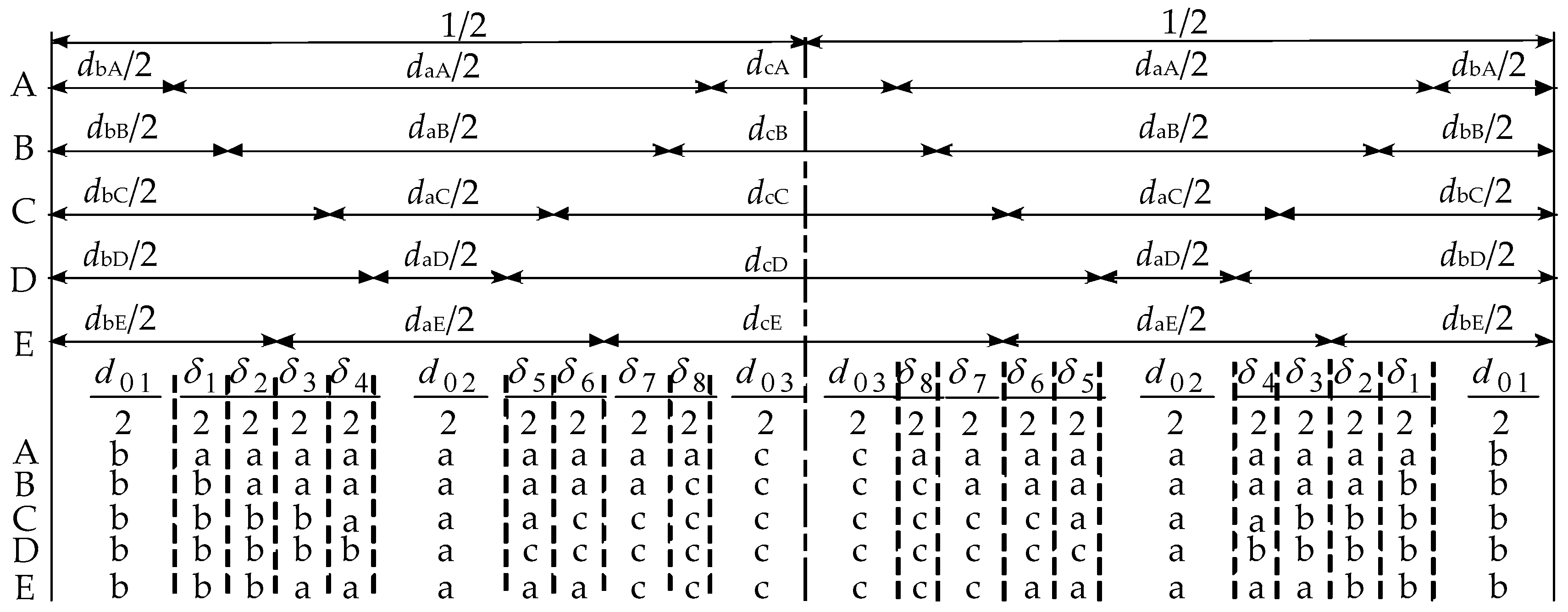
5.1. Decomposition and Simplification of Duty Cycles of the Three-to-Five Phase DMC

From Equation (1), the relationships between line-to-line output voltages and phase input voltages can be obtained as follows:
( u AB u BC u CD u DE u EA ) = ( d aA d aB d bA d bB d cA d cB d aB d aC d bB d bC d cB d cC d aC d aD d bC d bD d cC d cD d aD d aE d bD d bE d cD d cE d aE d aA d bE d bA d cE d cA ) ( u a u b u c )
Equation (25) shows that the line-to-line output voltages only depend on the difference between the two duty cycles. From Equation (23), which gives 15 duty cycles of switches, the difference beween the two duty cycles in Equation (25) is irrelevant to D0. For instance, uAB, uBC, uCD, uDE, and uEA only depend on DAB(DADB), DBC(DDC), DCD(DCDD), DDE(DDDE), and DEA(DEDA). According to the geometrical representation proposed in [17], five duty cycle vectors (DA, DB, DC, DD, DE) of the three-to-five phase DMC can be decomposed, as shown in Figure 2a.
As shown in Figure 2a, there is an equilateral triangle and its height is 1. The points represent the ends of five duty cycle vectors (DA, DB, DC, DD, and DE). The size of the duty cycles is the distance between each point and the equilateral triangle’s edge. Thus, duty cycles of 15 switches are obtained. By the example given in Figure 2a, the constraint on the angle of the input current is expressed as −π/6 ≤ βi < π/6, while the relationships between the five output voltages are expressed as uD < uC < uE < uB < uA. DD, DC, DE, DB, and DA are arranged sequentially in the positive direction of the βi. The 15 duty cycles in the modulation matrix can be expressed by 12 differences in duty cycles, and the relationships are as follows:”
{ d aA = d aD + ( d aC d aD ) + ( d aE d aC ) + ( d aB d aE ) + ( d aA d aB ) ; d aE = d aD + ( d aC d aD ) + ( d aE d aC ) ; d aB = d aD + ( d aC d aD ) + ( d aE d aC ) + ( d aB d aE ) ; d aC = d aD + ( d aC d aD ) ; d aD = d aD ; d bA = d bA ; d bB = d bA + ( d bB d bA ) ; d bC = d bA + ( d bB d bA ) + ( d bE d bB ) + ( d bC d bE ) ; d bD = d bA + ( d bB d bA ) + ( d bE d bB ) + ( d bC d bE ) + ( d bD d bC ) ; d bE = d bA + ( d bB d bA ) + ( d bE d bB ) ; d cA = d cA ; d cB = d cA + ( d cB d cA ) ; d cC = d cA + ( d cB d cA ) + ( d cE d cB ) + ( d cC d cE ) ; d cD = d cA + ( d cB d cA ) + ( d cE d cB ) + ( d cC d cE ) + ( d cD d cC ) ; d cE = d cA + ( d cB d cA ) + ( d cE d cB ) .
Given the known geometric properties of equilateral triangles, it is easy to obtain the following relation:
d aC d aD = ( d bD d bC ) + ( d cD d cC ) d aE d aC = ( d bC d bE ) + ( d cC d cE ) d aB d aE = ( d bE d bB ) + ( d cE d cB ) d aA d aB = ( d bB d bA ) + ( d cB d cA ) .
Taking Equation (27) into account, 15 duty cycles of the three-to-five phase DMC can be gained using eight differences in duty cycles, as shown in Figure 2b. Then, the eight differences in duty cycles can be redefined as follows:
δ 1 = d bB d bA ; δ 2 = d bE d bB ; δ 3 = d bC d bE ; δ 4 = d bD d bC ; δ 5 = d cD d cC ; δ 6 = d cC d cE ; δ 7 = d cE d cB ; δ 8 = d cB d cA .
Then, defining the equalities daD = doa, dbA = dob, and dcA = doc, and substituting Equations (27) and (28) into Equation (26) leads to
{ d aA = d oa + δ 1 + δ 2 + δ 3 + δ 4 + δ 5 + δ 6 + δ 7 + δ 8 ; d aB = d oa + δ 2 + δ 3 + δ 4 + δ 5 + δ 6 + δ 7 ; d aC = d oa + δ 4 + δ 5 ; d aD = d oa ; d aE = d oa + δ 3 + δ 4 + δ 5 + δ 6 ; d bA = d ob ; d bB = d ob + δ 1 ; d bC = d ob + δ 1 + δ 2 + δ 3 ; d bD = d ob + δ 1 + δ 2 + δ 3 + δ 4 ; d bE = d ob + δ 1 + δ 2 ; d cA = d oc ; d cB = d oc + δ 8 ; d cC = d oc + δ 6 + δ 7 + δ 8 ; d cD = d oc + δ 5 + δ 6 + δ 7 + δ 8 ; d cE = d oc + δ 7 + δ 8 .
Since the average value of the output voltages in one switching period is decided by the turn-on time of switches rather than the order of the switching sequence, the method in this paper rearranges the switching sequence, as given by Equation (29). Therefore, the arrangement of the switching sequence can be expressed as shown in Figure 3.

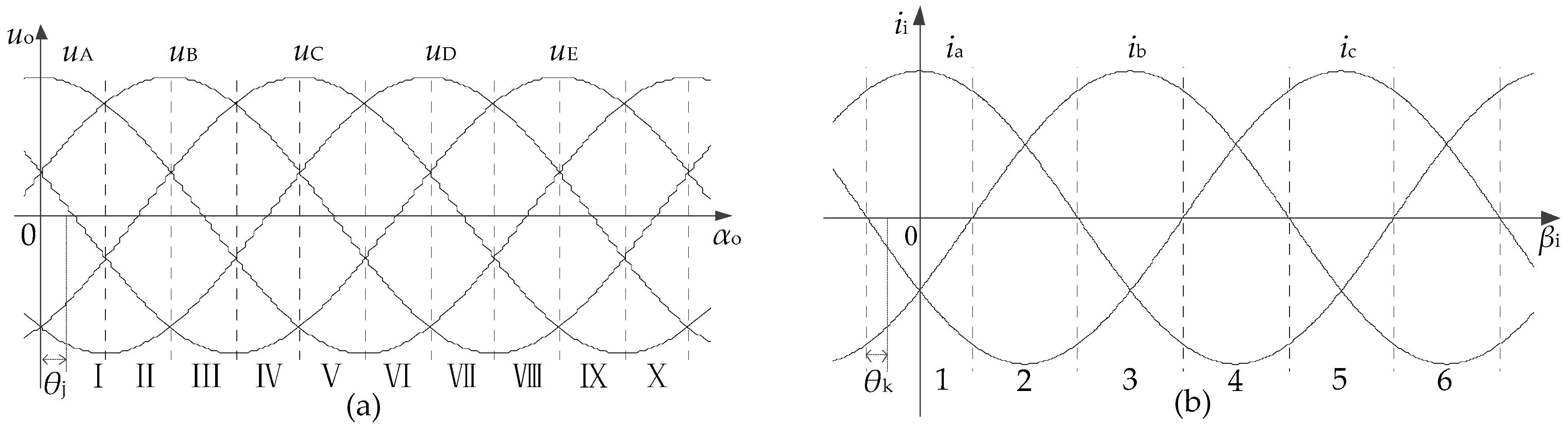
5.2. Segment Partition for Output Voltage and Input Current

As shown in Figure 2, the decomposition and simplification of the duty cycles will not be changed when −π/6 ≤ βi < π/6 and the relationship between the five output voltages does not change. Therefore, one period of input currents can be divided into six segments, while one period of expected five output voltages can be divided into 10 segments, as shown in Figure 4, where θj (0 ≤ θj < π/5) and θk (0 ≤ θk < π/3) are the relative position angles of the output voltage and input current in each segment, respectively.

5.3. General Expression of the Recombined Duty Cycles

The case illustrated in Figure 2 refers to the vectors of output voltage and input current lying in the corresponding sector 1, while θj = αo and θk = βi + π/6. By substituting Equation (23) into Equation (28), the expressions of eight recombined duty cycles can be obtained as follows:
{ δ 1 = 4 3 q sin π 5 sin ( π 5 θ j ) cos ( θ k + π 6 ) ; δ 2 = 4 3 q sin 2 π 5 sin θ j cos ( θ k + π 6 ) ; δ 3 = 4 3 q sin 2 π 5 sin ( π 5 θ j ) cos ( θ k + π 6 ) ; δ 4 = 4 3 q sin π 5 sin θ j cos ( θ k + π 6 ) ; δ 5 = 4 3 q sin π 5 sin θ j cos ( θ k π 2 ) ; δ 6 = 4 3 q sin 2 π 5 sin ( π 5 θ j ) cos ( θ k π 2 ) ; δ 7 = 4 3 q sin 2 π 5 sin θ j cos ( θ k π 2 ) ; δ 8 = 4 3 q sin π 5 sin ( π 5 θ j ) cos ( θ k π 2 ) ;
where θj = αo − (s − 1)π/5, θk = βi − (t − 1)π/3 + π/6, and s and t represent the segment numbers of the output voltage and input current, respectively, as shown in Figure 4.
The expressions of eight recombined duty cycles in other segment combinations also can be required, and are related to the parity of the sum of the input current and the output voltage segment. The expressions of the duty cycles are shown in Equation (30) when the sum of segments is even, while they are shown in Equation (31) when the sum is odd. The relationship between odd (denoted by δ’) and even (denoted by δ) can be expressed as follows:
δ 1 = δ 4 ; δ 2 = δ 3 ; δ 3 = δ 2 ; δ 4 = δ 1 ; δ 5 = δ 8 ; δ 6 = δ 7 ; δ 7 = δ 6 ; δ 8 = δ 5 .
Due to the constraint daX + dbX + dcX = 1 on all duty cycles, the duty cycle of the zero space vector can be obtained:
d 0 = d 01 + d 02 + d 03 = 1 ( δ 1 + δ 2 + δ 3 + δ 4 + δ 5 + δ 6 + δ 7 + δ 8 )
As seen from Equations (30)–(32), all active duty cycles and the zero duty cycle would be obtained easily if output voltages and input currents could be received. Thus, the method of SVPWM based on DCSV presented in this paper is simpler than the traditional SVPWM.

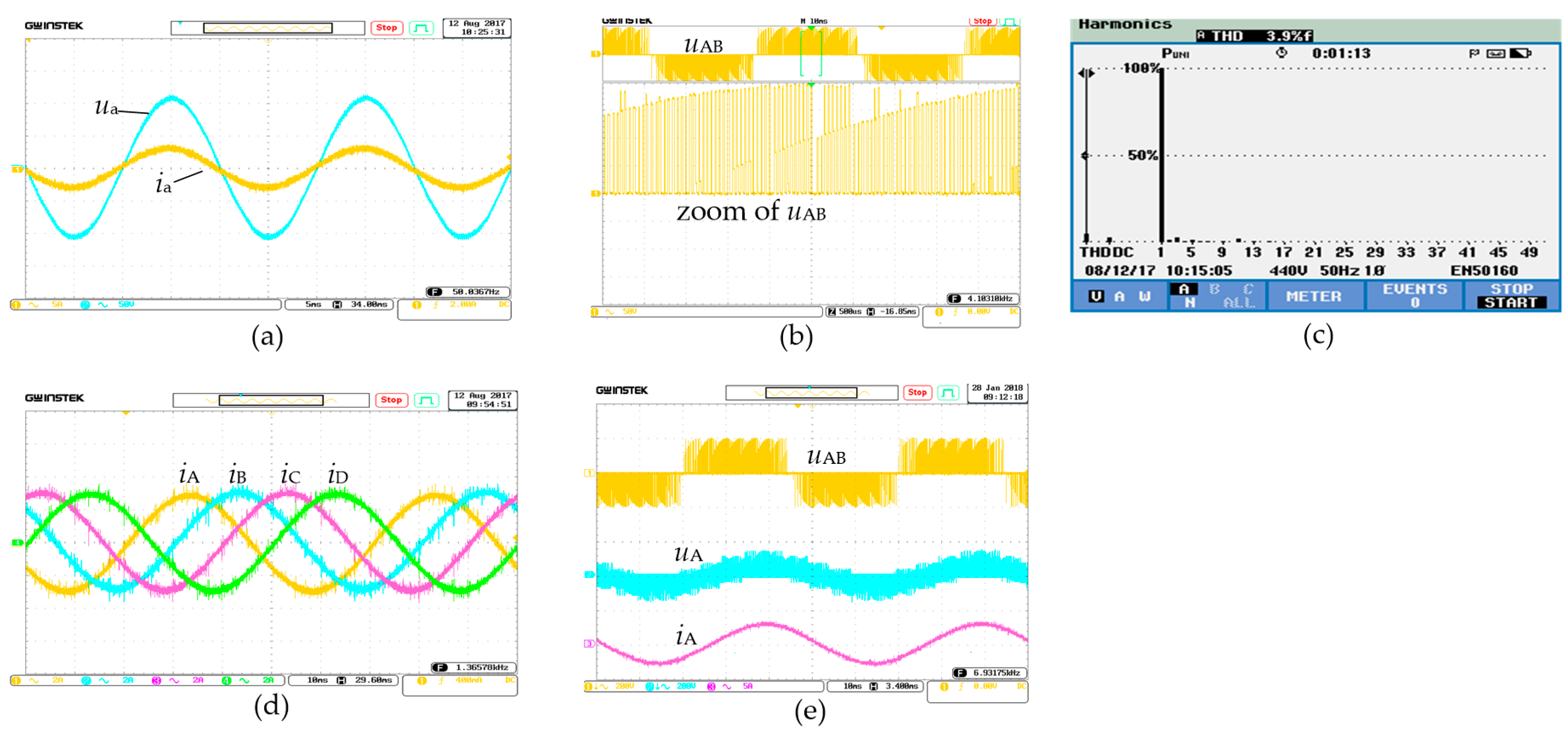
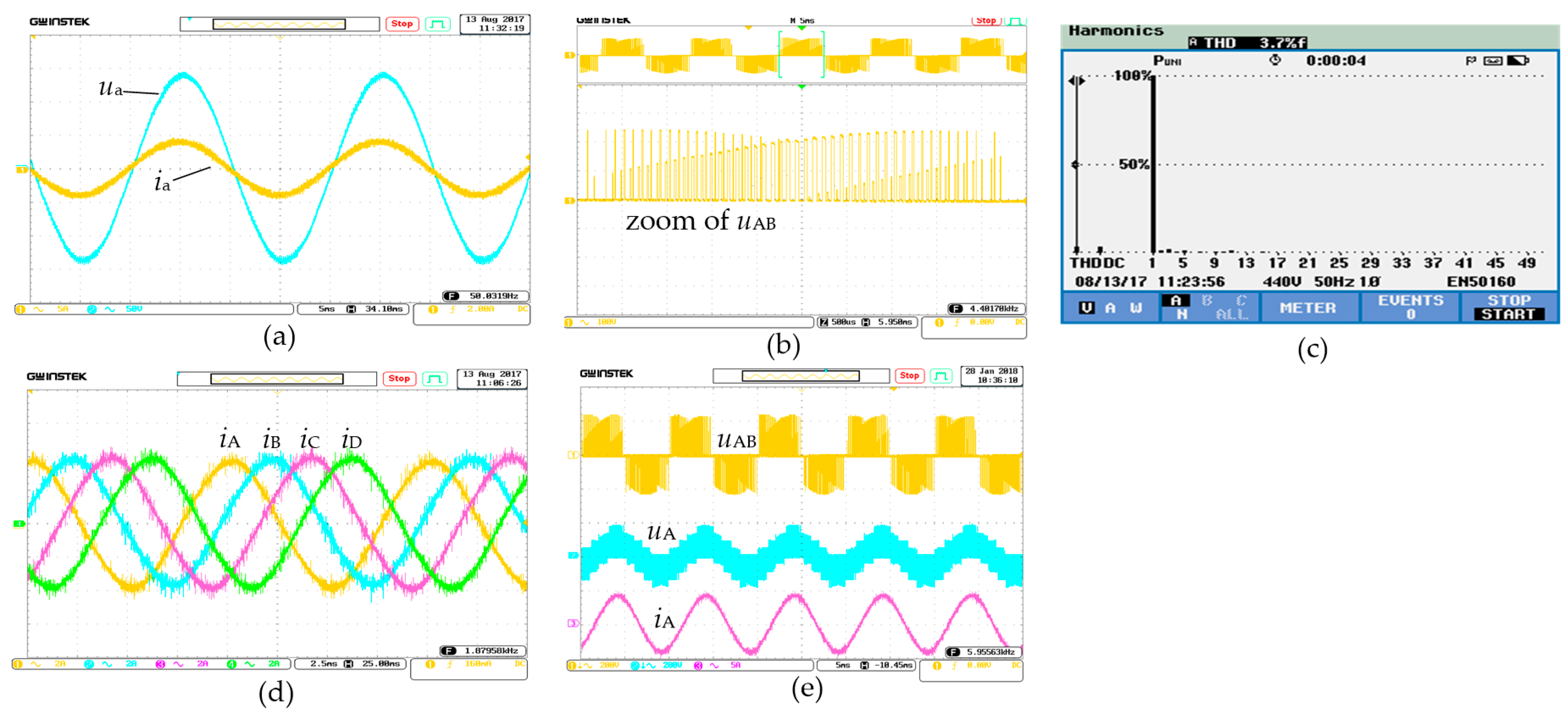
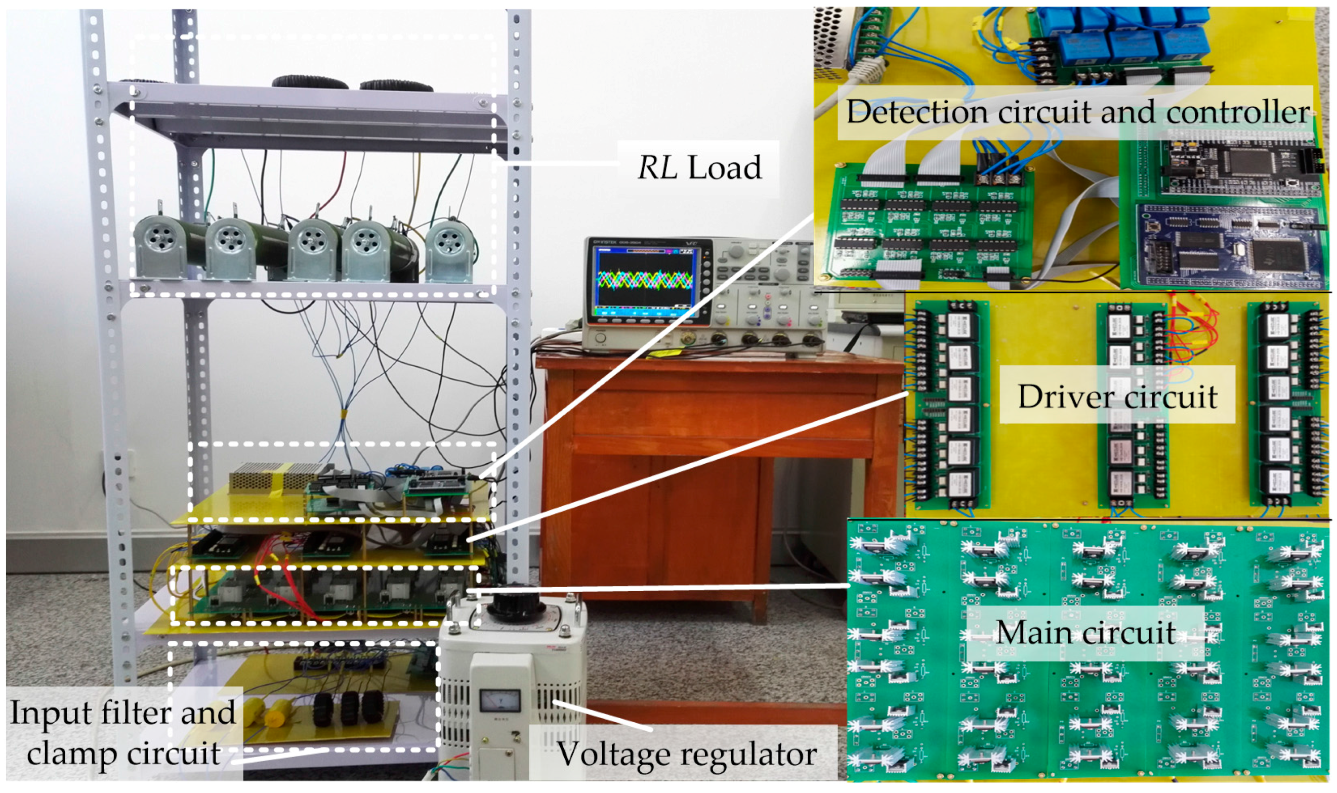
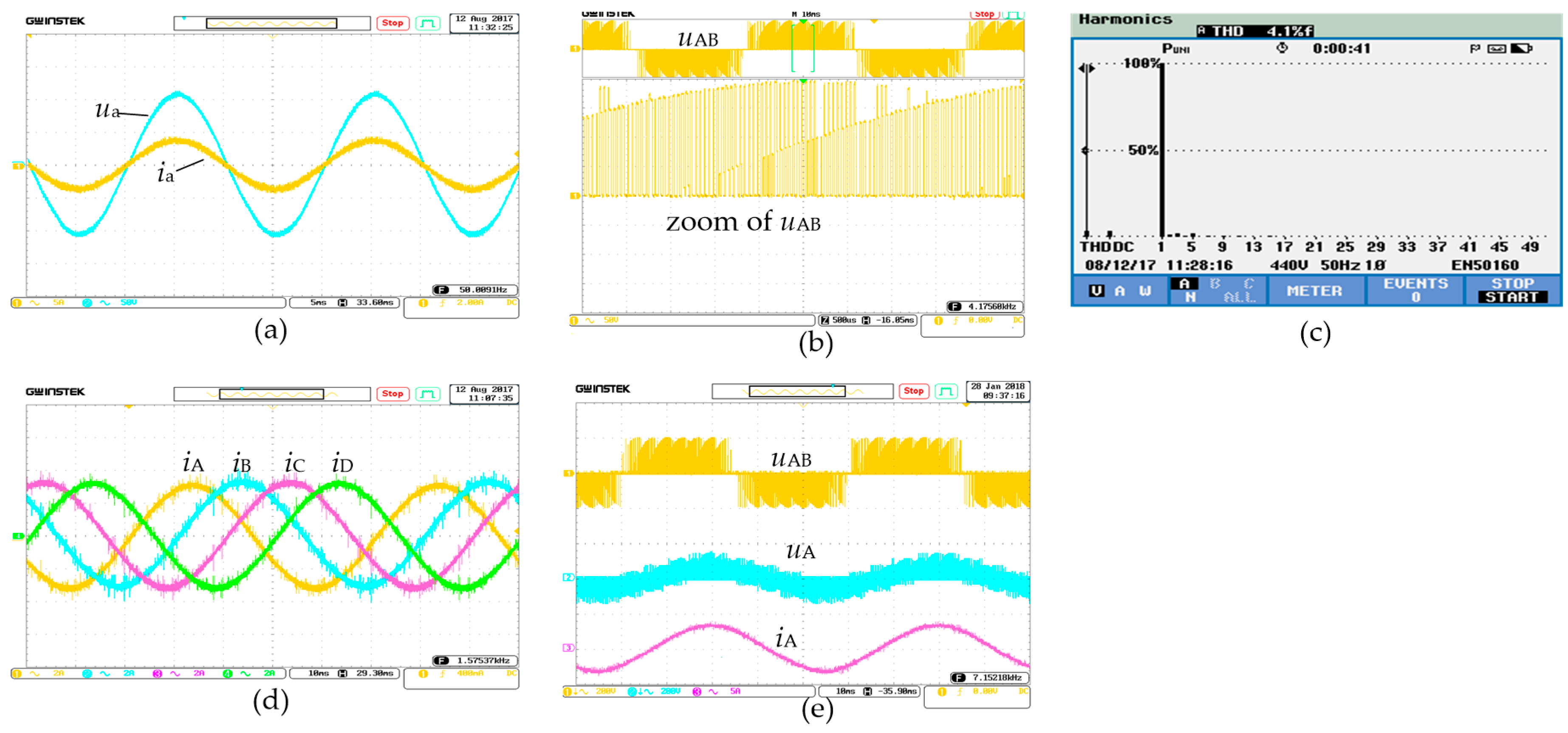
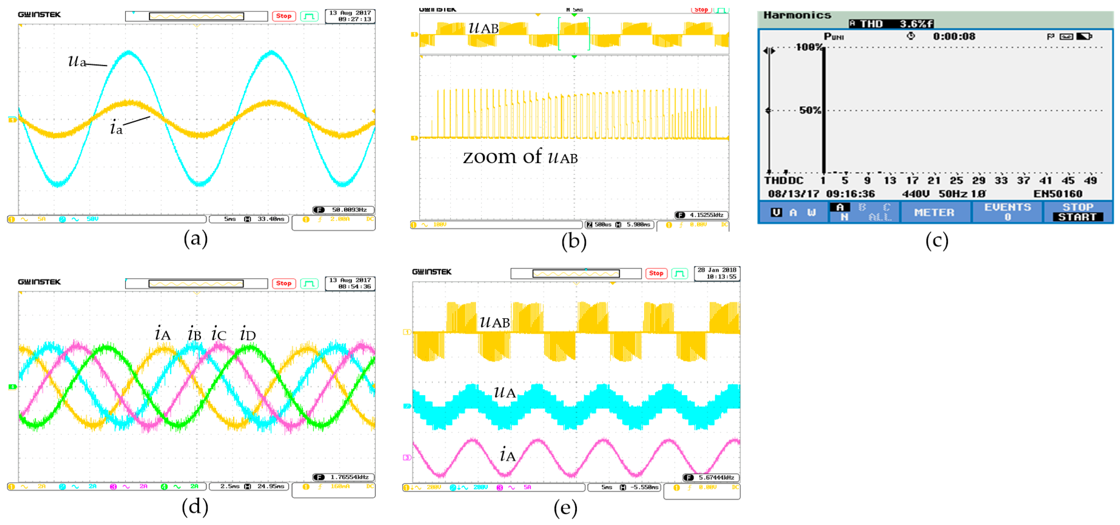
6. Experimental Results

To validate the accuracy and feasibility of the proposed modulation strategy, the DMC topology was built in the laboratory, as shown in Figure 5. The control system was implemented using the 32-bit digital signal processor (DSP) TMS320F28335 for calculating modulation waves and the field programmable gate array (FPGA) XC6SLX9 for implementing the switching sequences and the commutation process. Metal-oxide-semiconductor field-effect transistor (MOSFET) power switches were used to implement the power circuit. The MOSFET model was 2SK1940, with maximal turn-on and turn-off times of 135 ns and 330 ns, respectively. Therefore, the dead time was set to 500 ns in the program. In the experiment, the reference output voltage as set in the program beforehand. The DSP was applied to collect the input voltage, and generate PWM signals according to the modulation strategy. PWM signals were transmitted from the DSP to the FPGA, and four-step commutation [21] was achieved through logic programming in the FPGA. The clamp circuit was designed to protect the DMC against overvoltage of the input and/or output of the matrix converter. Experimental tests were carried out using a three-phase power supply (fin = 50 Hz). The input filter’s parameters were R = 2 Ω, Lf = 0.2 mH, and Cf = 20 μF, and the five-phase loads were five-phase resistance–inductance (RL) balanced loads (R = 16 Ω, L = 12 mH). The switching frequency of the bidirectional power switch was fixed at 10 kHz.
The experiments were divided into four cases. In one case, the input phase voltage value Uin was 80 Vrms, the output voltage frequency fout was 20 Hz, and the voltage transfer ratio (VTR) was 0.5. The experimental waveforms are shown in Figure 6. The input phase voltage ua and input phase current ia in Figure 6a clearly show the unity power factor at the input side. However, there is a displacement angle between the input voltage and input current because of the input LC filter. Figure 6b shows the waveforms of the line-to-line output voltage uAB and zoom of uAB. Figure 6c shows the fast Fourier transform (FFT) analysis of uAB, and the output voltage total harmonic distortion (THD) is 8%. It is evident that the output line-to-line voltage contains very few low-order harmonics. Figure 6d shows the output currents, which are balanced sinusoidal and symmetrical waveforms. From Figure 6b–d, it is confirmed that the fundamental output voltages are sinusoidal and symmetrical. Figure 6e shows the output line-to-line voltage uAB, output phase voltage uA and output phase current iA, synchronously. There is a displacement angle between uAB and uA, which is about 54°. There is also a small displacement angle between uA and iA because of the resistance–inductance load.
Figure 7 shows the experimental results with Uin = 80 Vrms, fout = 20 Hz, and q = 0.6. The waveforms in Figure 7 are similar to those in Figure 6, but the amplitude of input and output currents is just slightly larger because the VTR was changed from 0.5 to 0.6. It is clear that the proposed method has the ability to control the output voltage magnitude.
For Uin = 100 Vrms and fout = 100 Hz, experimental results are shown in Figure 8 and Figure 9 with different VTRs of 0.5 and 0.6, respectively. Compared with Figure 6 and Figure 7, the biggest difference is in the waveforms shown in Figure 8b,d,e and Figure 9b,d,e, because the output frequency is changed from 20 Hz to 100 Hz. It is clear that the proposed method has the ability to control the output voltage frequency to coincide with the reference values.
From the above experimental results, it is evident that performance of the three-to-five phase DMC with the proposed method in this paper can be achieved.

7. Conclusions

In this paper, a novel method for the three-to-five phase direct matrix converter, named the DCSV strategy, was proposed. For this method, the general expression of the turn-on time of each switch was obtained. This method is of universal significance as it can realize different modulation strategies through suitable use of the zero configurations. In addition, an original SVPWM strategy based on the proposed DCSV was derived. The DCSV also has the ability to realize a reference load voltage of up to 0.7886 for the input voltage in the linear modulation region. A symmetrical switching sequence was obtained by using zero vectors and active vectors, and the fewest commutations were realized in one switching period. Finally, the feasibility of this novel method was validated through experimental results.

Acknowledgments

This research is funded by National Key R&D Program of China under grant number 2017YFB0903300.

Author Contributions

Rutian Wang and Xue Wang conceived the theory; Chuang Liu performed the experiments and analyzed the data; Xiwen Gao contributed materials and analysis tools; Rutian Wang and Xue Wang wrote the paper.

Conflicts of Interest

The authors declare no conflict of interest.

References

  1. Huang, X.; Goodman, A.; Gerada, C.; Fang, Y.; Lu, Q. Design of a Five-Phase Brushless DC Motor for a Safety Critical Aerospace Application. IEEE Trans. Ind. Electron. 2012, 59, 3532–3541. [Google Scholar] [CrossRef]
  2. Levi, E.; Bodo, N.; Dordevic, O.; Dordevic, O.; Jones, M. Recent Advances in Power Electronic Converter Control for Multiphase Drive Systems. In Proceedings of the IEEE Electrical Machines Design Control and Diagnosis, Paris, France, 11–12 March 2013; pp. 158–167. [Google Scholar]
  3. Empringham, L.; Kolar, J.W.; Rodriguez, J.; Wheeler, P.W.; Clare, J.C. Technological Issues and Industrial Application of Matrix Converters: A Review. IEEE Trans. Ind. Electron. 2013, 60, 4260–4271. [Google Scholar] [CrossRef]
  4. Levi, E. Multilevel Multiphase Drive Systems-Topologies and PWM Control. In Proceedings of the IEEE International Conference Electric Machines and Drives, Chicago, IL, USA, 12–15 May 2013; pp. 1500–1508. [Google Scholar]
  5. Ahmed, S.M.; Abu-Rub, H.; Salarti, Z.; Rivera, M.; Ellabban, O. Generalized Carrier Based Pulse Width Modulation Technique for a Three to N-Phase Dual Matrix Converter. In Proceedings of the International Conference Industrial Electronics Society, Dallas, TX, USA, 29 October–1 November 2014; pp. 3298–3304. [Google Scholar]
  6. Dabour, S.M.; Allam, S.M.; Rashad, E.M. Indirect Space-Vector PWM Technique for Three to Nine Phase Matrix Converters. In Proceedings of the GCC Conference and Exhibition, Muscat, Oman, 1–4 February 2015. [Google Scholar]
  7. Omrani, K.; Dami, M.A.; Jemli, M. Three to Six-Phase Direct Matrix Converters. In Proceedings of the International Conference Renewable Energy Congress, Hammamet, Tunisia, 1–5 March 2016. [Google Scholar]
  8. Iqbal, A.; Rahman, K.; Alammari, R.; Abu-Rub, H. Space Vector PWM for a Three-Phase to Six-Phase Direct AC/AC Converter. In Proceedings of the International Conference Industrial Technology, Seville, Spain, 17–19 March 2015; pp. 1179–1184. [Google Scholar]
  9. Ahmed, S.M.; Iqbal, A.; Abu-Rub, H. Simple Carrier-Based PWM Technique for a Three-to-Nine-Phase Direct AC-AC Converter. IEEE Trans. Ind. Electron. 2011, 58, 5014–5023. [Google Scholar]
  10. Ahmed, S.M.; Salam, Z.; Abu-Rub, H. An improved Space Vector Modulation for a Three-to-Seven-Phase Matrix Converter with Reduced Number of Switching Vectors. IEEE Trans. Ind. Electron. 2015, 62, 3327–3337. [Google Scholar] [CrossRef]
  11. Rodriguez, J.; Rivera, M.; Kolar, J.W.; Wheeler, P.W. A Review of Control and Modulation Methods for Matrix Converters. IEEE Trans. Ind. Electron. 2012, 59, 58–70. [Google Scholar] [CrossRef]
  12. Lozano-Garcia, J.M.; Ramirez, J.M. Voltage Compensator Based on a Direct Matrix Converter without Energy Storage. IET Power Electron. 2014, 8, 321–332. [Google Scholar] [CrossRef]
  13. Ahmed, S.M.; Iqbal, A.; Abu-Rub, H. Generalized Duty-Ratio-Based Pulsewidth Modulation Technique for a Three-to-k Phase Matrix Converter. IEEE Trans. Ind. Electron. 2011, 58, 3925–3937. [Google Scholar] [CrossRef]
  14. Ahmed, S.M.; Iqbal, A.; Abu-Rub, H. Space Vector PWM Technique for a Novel Three-to-Five Phase Matrix Converter. In Proceedings of the IEEE Energy Conversion Congress and Exposition, Atlanta, GA, USA, 12–16 September 2010; pp. 1875–1880. [Google Scholar]
  15. Iqbal, A.; Ahmed, S.M.; Abu-Rub, H. Space Vector PWM Technique for a Three-to-Five Matrix Converter. IEEE Trans. Ind. Appl. 2012, 48, 696–707. [Google Scholar] [CrossRef]
  16. Dabour, S.M.; Allam, S.M.; Rashad, E.M. A Simple CB-PWM Technique for Five-Phase Matrix Converters Including Over-Modulation Mode. In Proceedings of the GCC Conference and Exhibition, Muscat, Oman, 1–4 February 2015. [Google Scholar]
  17. Nguyen, T.D.; Lee, H. Development of a Three-to-Five-Phase Indirect Matrix Converter with Carrier-Based PWM Based on Space-Vector Modulation Analysis. IEEE Trans. Ind. Electron. 2016, 63, 13–24. [Google Scholar] [CrossRef]
  18. Novotny, D.W.; Lipo, T.A. Vector Control and Dynamics of AC Drives; Oxford University Press: Oxford, UK, 1996. [Google Scholar]
  19. Ryu, H.M.; Kim, J.W.; Sul, S.K. Synchronous Frame Current Control of Multi-Phase Synchronous Motor, Part I: Modeling and Current Control Based on Multiple d-q Spaces Concept under Balanced Condition. In Proceedings of the IEEE International Conference Industry Applications Society Annual Meeting, Seoul, Korea, 3–7 October 2004; pp. 56–63. [Google Scholar]
  20. Casadei, D.; Serra, G.; Tani, A.; Zarri, L. Matrix Converter Modulation Strategies: A New General Approach Based on Space-Vector Representation of the Switch State. IEEE Trans. Ind. Electron. 2002, 49, 370–381. [Google Scholar] [CrossRef]
  21. An, X.; Lin, H.; Wang, X.W. Analysis of Commutation Strategy for Matrix Converter Based on FPGA. Power Electron. 2011, 45, 20–22. [Google Scholar]
Figure 1. Topology of a three-to-five phase MC.
Energies 11 00370 g001
Figure 2. Decomposition and simplification of duty cycles of the three-to-five phase DMC: (a) decomposition of five duty-cycle space vectors; (b) simplification of a decomposed duty cycle.
Energies 11 00370 g002
Figure 3. Arrangement of a switching sequence.
Energies 11 00370 g003
Figure 4. Segment partition (a) output voltages and (b) input currents.
Energies 11 00370 g004
Figure 5. Experimental prototype.
Energies 11 00370 g005
Figure 6. Experimental waveforms with Uin = 80 Vrms, fout = 20 Hz, and q = 0.5: (a) input voltage ua and input current ia; (b) output line-to-line voltage uAB and zoom of uAB; (c) the FFT analysis of the uAB; (d) output currents iA, iB, iC, iD; (e) output line-to-line voltage uAB, output phase voltage uA, and output phase current iA.
Energies 11 00370 g006
Figure 7. Experimental waveforms with Uin = 80 Vrms, fout = 20 Hz, and q = 0.6: (a) input voltage ua and input current ia; (b) output line-to-line voltage uAB and zoom of uAB; (c) the FFT analysis of the uAB; (d) output currents iA, iB, iC, iD; (e) output line-to-line voltage uAB, output phase voltage uA, and output phase current iA.
Energies 11 00370 g007
Figure 8. Experimental waveforms with Uin = 100 Vrms, fout = 100 Hz, and q = 0.5: (a) input voltage ua and input current ia; (b) output line-to-line voltage uAB and zoom of uAB; (c) the FFT analysis of the uAB; (d) output currents iA, iB, iC, iD; (e) output line-to-line voltage uAB, output phase voltage uA, and output phase current iA.
Energies 11 00370 g008
Figure 9. Experimental waveforms with Uin = 100 Vrms, fout = 100 Hz, and q = 0.6: (a) input voltage ua and input current ia; (b) output line-to-line voltage uAB and zoom of uAB; (c) the FFT analysis of the uAB; (d) output currents iA, iB, iC, iD; (e) output line-to-line voltage uAB, output phase voltage uA, and output phase current iA.
Energies 11 00370 g009

