1. Introduction
The reliability of electronic power converters is a very important feature in industrial applications. Nevertheless, conversion systems used in industry are subject to different stress types, including temperature variation, vibration, radiation and humidity [
1,
2,
3,
4,
5,
6]. The capacitor is the weakest component in power converters and is responsible for approximately 30% of failures during power conversion [
7].
Generally, there are various types of power converters that exert voltage vectors into the load application, such as single voltage source inverters (S-VSI) [
8,
9], two-level voltage source inverters (2L-VSI), multilevel inverters (MLIs) [
10,
11], and matrix converters (MCs) [
12,
13,
14]. Among them, the 2L-VSI, shown in
Figure 1, is the most common topology used in industry [
15]. The DC-link capacitor is a vital component in this topology as it compensates for the power difference between the input and the output. It also maintains the DC voltage around a necessary level. However, due to the high-frequency ripple current flowing through the DC-link, the capacitor endures constant stress, resulting in a decreased life-span. To overcome this issue, several capacitors in real applications are paralleled, allowing them to share the ripple current and decrease the stress on each component. As a result, the volume of the whole system is influenced mainly by the bulky DC-link capacitor block.
The power transistors are also vulnerable parts of power converters. Switching over the intervals with high current rates causes the power loss of each transistor. Selection of a modulation strategy to synthesize output voltages relies on switching losses, ease of numerical implementation, desired linearity, and modulation range. There are two common carrier types: Continuous based modulation (CPWM), such as sine pulse-width modulation (SPWM) and space vector pulse-width modulation (SVPWM) and discontinuous based modulation, namely discontinuous pulse-width modulation (DPWM). Among these two types, the DPWM has higher capability of diminishing the stress on transistors and minimizing power loss. Moreover, the DPWM is advantageous regarding improved system efficiency [
16]. For conventional DPWM schemes [
17,
18,
19,
20] power loss is reduced by 33%.
The main idea of the DPWM is to stop operating each power transistor sequentially during a certain amount of time, usually equal to 60 electrical degrees or 1/3 of the fundamental period, to reduce the stress on the power transistors. Moreover, implementing the DPWM into different systems can also solve other problems common for power electronics. In References [
21,
22], novel DPWM methods were respectively used for the neutral-point voltage control of the Neutral-Point Clamped (NPC) converter and the Vienna-rectifier. Additionally, some DPWM methods can be used to reduce the common-mode voltage (CMV) of power converters [
23]. However, the aforementioned methods do not minimize the stress on DC-link capacitors. A system with reduced power loss of the switches and minimized DC-link ripple would result in increased stability and reliability.
There have been several studies done to reduce the ripple current of the DC-link capacitor in systems using DPWM. Several works [
24,
25,
26] found a novel DPWM algorithm for the back-to-back converter. In addition, Zhang et al. [
27] introduced the carrier interleaving method between two paralleled VSIs. Moreover, in [
28] an optimal switching pattern was proposed for the T-type MLI with the CPWM. Despite the outstanding performance of these methods, they can only be used in particular configurations utilizing a few converters and thus, cannot be applied to a single 2L-VSI.
This paper proposes a PWM phase-shift method to reduce the DC-link ripple current in a single two-level VSI with the conventional carrier-based DPWM. The efficacy of the proposed technique is verified via simulations and experiments.
The paper is organized as follows: The lifetime model of the DC-link capacitor is presented in
Section 2.
Section 3 concentrates on the discussion of the conventional DPWM, whereas
Section 4 provides the details on the proposed method. Simulation and experimental results are given in
Section 5 and
Section 6, respectively. Conclusions are drawn in
Section 7.
2. DC-Link Capacitor Lifetime
The lifetime is one of the most important parameters for DC-link capacitors. It depends on factors such as temperature, humidity, and vibration. [
2,
3,
4,
5]. The lifetime model of an electrolytic capacitor, used in this paper, is shown in Equation (1):
where
Lnom,
Vnom, and
Tnom are the nominal values of the lifetime, voltage, and temperature, respectively.
Vapp is the applied voltage and
Tcor is the core temperature of the capacitor.
n is a voltage stress coefficient.
In 2L-VSI, the voltage is maintained around a certain level and its fluctuations are relatively small, the lifetime is mainly determined by the core temperature:
where
Ta is the ambient temperature,
Rth is the case-ambient resistance of the capacitor,
Pd is the power dissipation or the thermal loss, caused by the ESR of the capacitor and estimated as follows:
where
IRMS is the RMS value of the ripple current, flowing through the capacitor.
Obviously, the lifetime of the capacitor is influenced by the ripple current, which results in power loss and temperature rise of ΔT. Therefore, the lifetime of the capacitor can be increased by reducing the ripple current flowing through it.
3. Conventional DPWM
To operate the VSI, there are two commonly used carrier-based methods, the CPWM and the DPWM. The former is advantageous in terms of implementation simplicity and stable AC-current quality, despite the change of the modulation index (MI). However, when the current of each phase reaches the maximum value, the power loss of the corresponding power switch is drastically increased. The DPWM allows one to diminish the power loss by stopping the operation of the power switches during the intervals with the maximum current. At that moment, the AC-current is modulated by the other two phases. Although there are several different DPWM methods, the conventional 60° DPWM is the most commonly used for the systems with the unity power factor.
The offset signal and the reference voltages of all three phases for the 60° DPWM are given in
Figure 2. The reference voltages are obtained by adding the offset voltage (
Voffset) to the sine signal. As can be seen from the figure, each phase is sequentially attached to the DC-bus at the moment when its instantaneous value is close to peak magnitude. The duty cycle of the clamped phase always 1 or 0, and therefore, the switches of the appropriate leg are contrarily locked ON or OFF.
Therefore, the pole reference voltages to be applied to the VSI are described by:
where
V*an,
V*bn and
V*cn are the instant pole reference voltages to be applied to the VSI, whereas
V*as,
V*bs and
V*cs are the instant reference voltages of each phase, respectively.
Voffset is the instant offset voltage used in the DPWM.
To obtain the offset voltage necessary for the DPWM, it is assumed that the pole reference voltages do not exceed
Vdc/2 as in:
Therefore, with this degree of freedom, the offset voltage is estimated:
where
Vmax and
Vmin are respectively the maximum and the minimum values among the phase reference voltages.
Then, the direction of the extremum phase is estimated as the sum of
Vmax and
Vmin, the offset voltage is calculated as follows [
10]:
Evidently, the pole reference voltages of each phase are obtained by changing the zero-sequence component, which is usually referred to as an offset voltage. As one of the phase references is being clamped to either bus of the DC-link, the power switches of the corresponsive leg do not operate and therefore there is no switching losses. Obviously, it is preferred that each phase is clamped when the maximum current passes through it.
4. Proposed DPWM
As previously mentioned, in the DPWM the pole reference voltage of the phase with the maximum amplitude is attached to the DC-bus and the corresponding power transistor is locked either ON or OFF. The DC-link ripple according to the switching pattern is shown in
Figure 3a. The A-phase is clamped to the negative DC-bus and the switching function of the corresponsive power switch is equal to 0. Since the switching frequency is much higher than the fundamental frequency of the VSI, the pole reference voltages are assumed to be constant values.
As can be observed from the figure, the instantaneous value of the DC-link current is determined by the superposition of the phase currents
ia,
ib,
ic and the dc source current
idc1:
where
Sa,
Sb and
Sc are the switching functions of the corresponding phases, defined as:
where
i represents one of the phases
a,
b or
c. Thus, according to Equation (5), the DC-link current is the product of three switching functions and three corresponding AC-currents.
In a conventional DPWM method with a single PWM, shown in
Figure 3a, the instantaneous value of the DC-link ripple current is described as
Obviously, with a switching function equal to 0, the corresponding current does not affect the DC-link current. Moreover, the maximum value of the ripple current is reached when all the switching functions are equal,
Sa =
Sb =
Sc, and the DC-link current is determined by the load current (
idc1) only. The root-mean-square (RMS) value of the DC-link current is evaluated as:
Considering the instant position of each phase, the time intervals
T1,
T2 and
T3 are estimated as:
where
Va,
Vb and
Vc are the pole reference voltages of the corresponding phases and
Vdc is the DC-link voltage. These components are represented as:
Then, the RMS of the DC-link current is evaluated as:
From
Figure 3a and Equation (14), it can be clearly seen that the DC source current (
idc1) contributes the most to the RMS value of the DC-link current. This issue can be solved if the switching functions of the three phases are not equal during
T3. From
Figure 3b, it is evident that this condition can be achieved by introducing a phase-shift between two non-clamped phase references. Thus, the
idc1 component can be removed from the RMS of the DC-link current, as illustrated in
Figure 3b. Then, the instantaneous values of the DC-link are:
the DC-link RMS is calculated as:
Obviously, for all the time intervals T1, T2 and T3, the idc1 component, which contributes the most to the DC-link current RMS, is subtracted from the phase currents. Therefore, the RMS is decreased by a simple phase shift between the non-clamped phases.
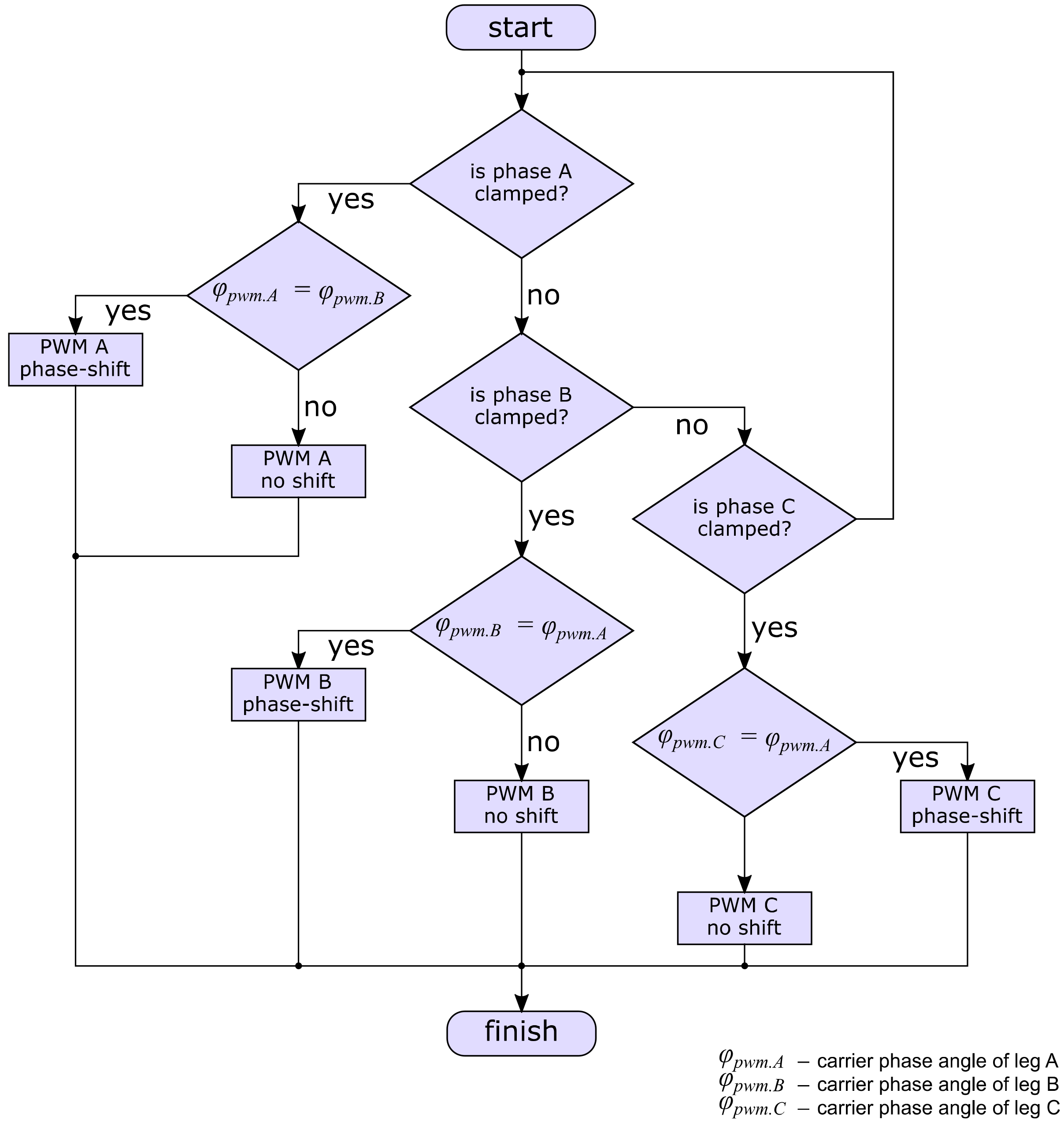
Hence, for the proposed method, there is always a 180° phase-shift between two active phases, e.g., when A-phase is being clamped to any of the DC-link buses, there is no PWM switching for the corresponding leg of the VSI, however, the phases B and C should have a 180° phase-shift between the PWM carriers.
In the VSI, the sudden change of a PWM carrier phase can cause disturbances to the AC-current quality. However, in a DPWM-based VSI, the phase-shift of a carrier can be fulfilled when there is no actual switching. In other words, when the corresponding phase is being clamped. As is evident from
Figure 2, the state of the clamped phases of the VSI is always in the same order. The next clamped phase after the phase
A is phase
C, then phase
B followed by the phase
A again. Thus, when the
A phase of the VSI is being clamped, the initial phase of the corresponding PWM carrier should be different from the initial phase of the PWM carrier for the
B phase. When
φpwm.A =
φpwm.B, it means there is no phase-shift between phases
A and
B. The flowchart of the proposed method is given in
Figure 4.
φpwm indicates the initial phase-shift angle of the corresponding phase.
5. Simulation Results
To confirm the validity of the proposed method, a simulation has been conducted via the MATLAB/SIMULINK environment using the PLECS toolbox. The circuit used for the simulation is the same as that given in
Figure 1. The simulation parameters are given in
Table 1.
Figure 5 illustrates the simulation results for the conventional CPWM method. The RMS of the DC-link ripple current is 10.2 A, the AC-current Total Harmonic Disturbance (THD) is 2.3% and the CMV is the highest compared to the other methods. The conventional DPWM method, given in
Figure 6, has the same profile of the DC-link current, but with better performance of the CMV. Obviously, when the proposed method is applied as shown in
Figure 7, the RMS value of the DC-link ripple current is decreased to 7.4 A, which is approximately 30% of the conventional method. The DC-link current reaches the load current gradually, as one of the non-clamped reference voltages reaches its maximum value. Moreover, with the proposed method, the CMV is also significantly improved as can be observed from
Figure 7. However, there is a drawback as the AC-current THD is increased from 2.9% of the conventional DPWM method to 3.7% of the proposed method. According to the IEEE standard 519-2014, the THD limit for systems with bus voltage less than 1 kV is 8%, thus, the proposed method can be applied in well-designed systems without exceeding the maximum THD [
29].
For the efficiency estimation, the switching losses (
PQ.sw) for all the methods are calculated as:
where
fsw is the switching frequency,
EON is a turn-on energy loss and
EOFF is turn-on energy loss. The switching losses of the diode (
PD.sw) are estimated considering the reverse-recovery energy loss
Err:
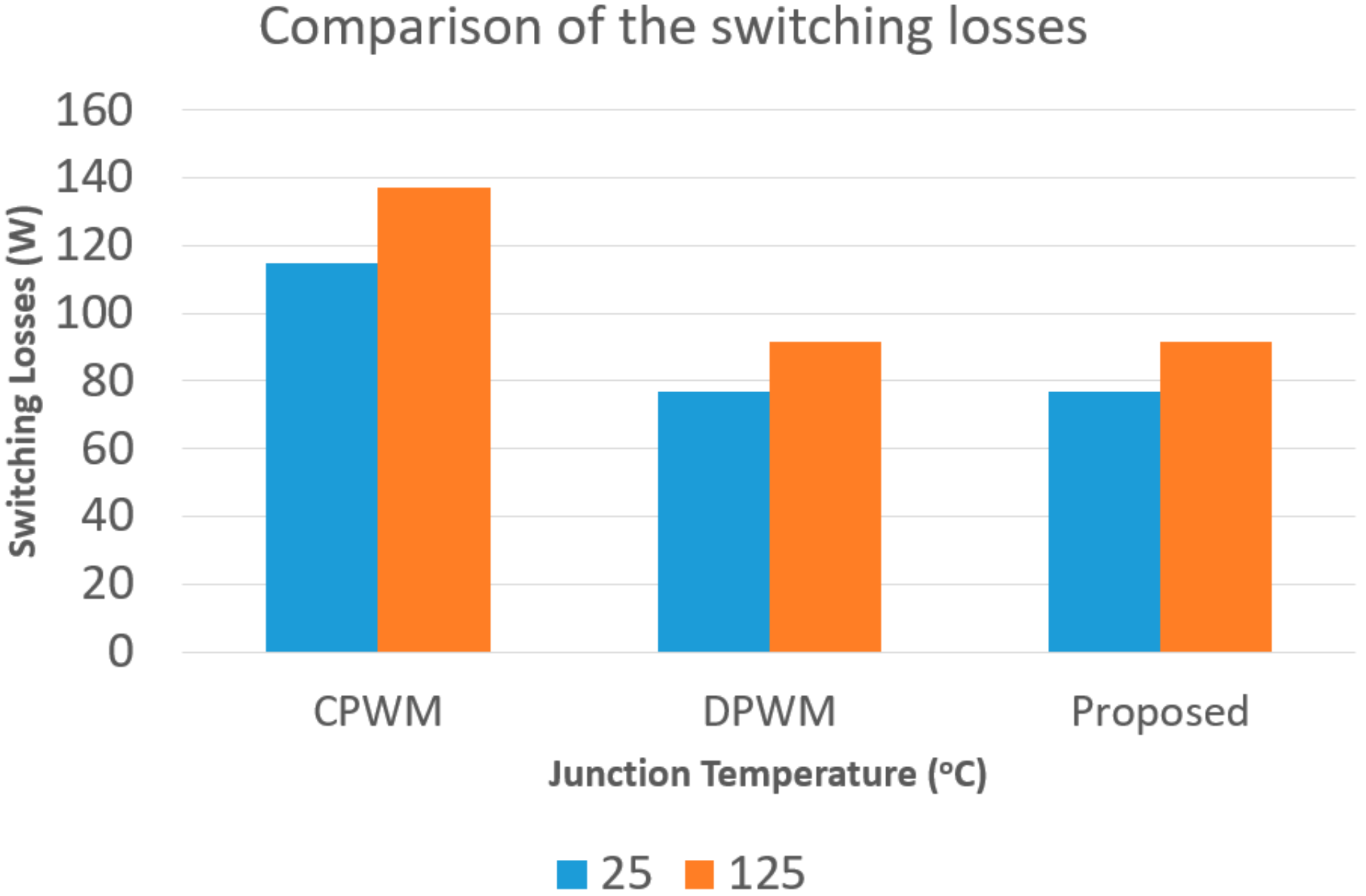
Figure 8 provides the switching losses comparison between the CPWM, DPWM and the proposed DPWM methods. The IGBT data used for the switching losses analysis was taken from the datasheet of the SK75MLI066T module and used in the experimental setup.
EON = 1.7 mJ/pulse,
EOFF = 2.8 mJ/pulse and
Err = 1.1 mJ/pulse.
The switching losses were evaluated for two different junction temperatures, 25 and 125 °C. From the figure, it is evident that the proposed method has identical performance with the conventional DPWM in terms of the switching losses. The switching losses of the two discontinuous methods were lower than those of the CPWM.
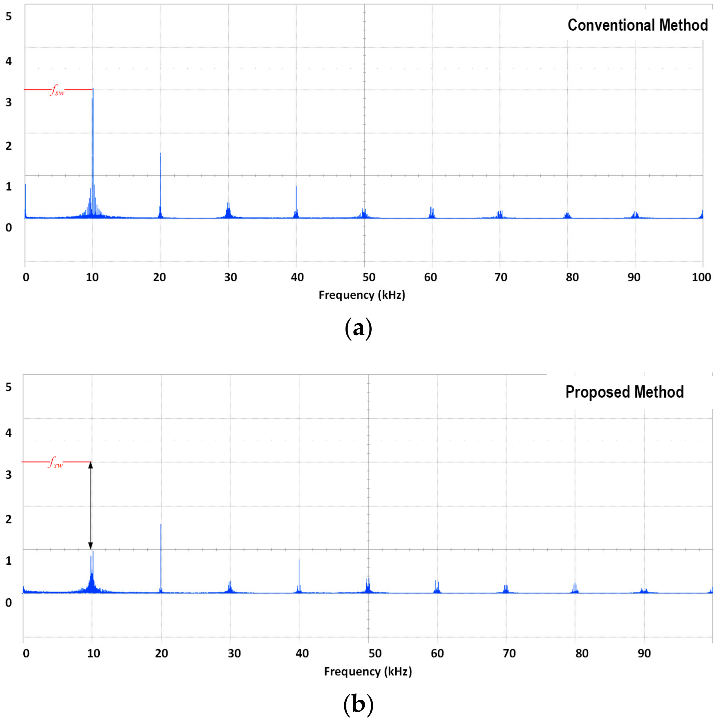
The frequency spectrum (FFT) of the DC-link ripple current and the CMV for the conventional and the proposed methods are shown in
Figure 9. As can be noticed, the amplitudes of the 1st and the 3rd harmonic components of the DC-link were reduced with the proposed method and the dominant 1st order harmonic was significantly diminished when the proposed method applied. Moreover, the 1st order harmonic of the CMV was also considerably reduced compared to that of the conventional method.
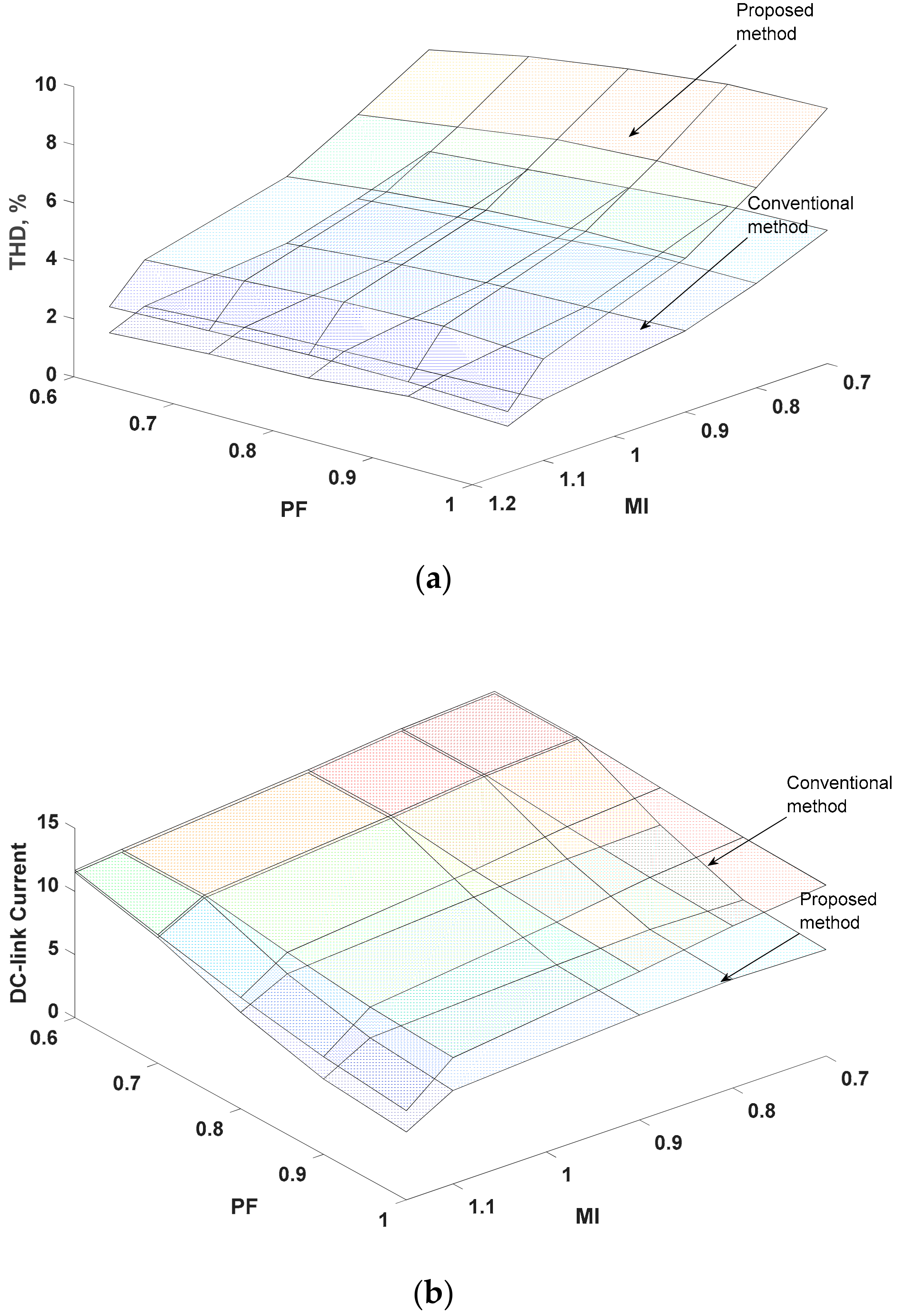
Further simulations were implemented to estimate the behavior of the proposed method for different conditions depending on the power factor (PF) and the modulation index (MI). As can be seen from
Figure 10a, the proposed method deteriorated the THD of the AC-current in the whole range of the MI and the PF. However, with the higher values of the MI, the difference in the THD between the proposed and the conventional methods decreased. Moreover, it is obvious from
Figure 10b that the DC-link ripple current can be reduced in a wide range of the PF and the MI. Nonetheless, the trade-off of the DC-link current reduction and the AC-current THD can be achieved at high MI with the PF close to unity.
6. Experimental Results
The experiment has been conducted to evaluate the performance of the proposed method. The experimental setup is given in
Figure 11. The experimental circuit was identical to that given in
Figure 1. A utility grid with the frequency 60 Hz and line-to-line voltage 110 V with the impedance 0.1 Ω was connected to the VSI through a 930 mH L-filter. The DC-link voltage was set to 300 V. To verify the THD of the AC-current, the power analyzer GT3000 by Yokogawa (Tokyo, Japan) was used.
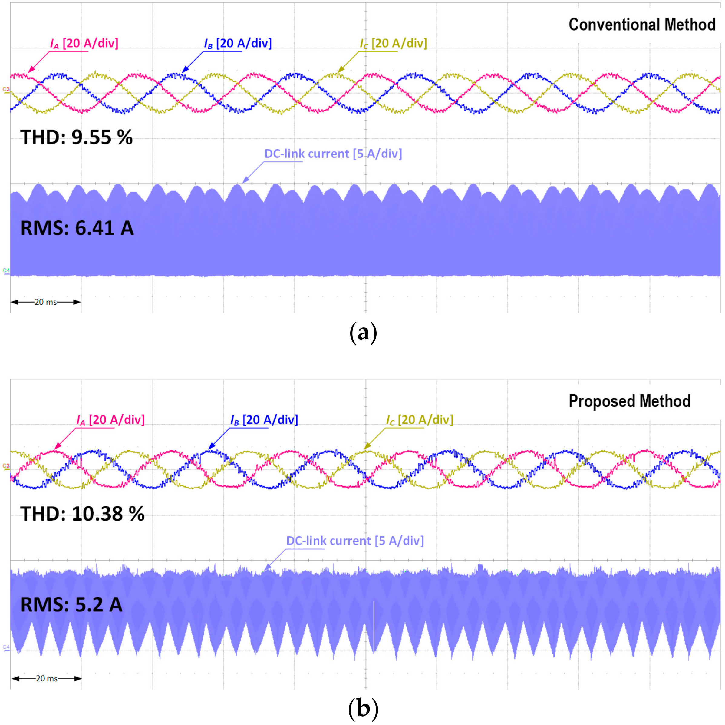
Figure 12,
Figure 13 and
Figure 14 show the experimental results of the conventional method and the proposed method. As can be seen from
Figure 12a,b, the profile of the DC-link ripple current RMS was reduced and the RMS value was decreased from 6.41 A in the conventional method, to 5.2 A in the proposed method. Moreover, as it is evident from the figures, the AC-current THD was slightly deteriorated by less than 1%. Furthermore, the proposed method was superior in terms of the CMV, as can be observed from
Figure 13a,b. Finally, the FFT of the DC-link ripple current is shown in
Figure 14a for the conventional method and
Figure 14b for the proposed method. Obviously, the 1st harmonic component was greatly reduced with the proposed algorithm compared to that of the conventional method.


