Article

Study on Insulation Breakdown Characteristics of Printed Circuit Board under Continuous Square Impulse Voltage

1
State Key Laboratory of Power Transmission Equipment & System Security and New Technology, School of Electrical Engineering, Chongqing University, Chongqing 400044, China
2
State Grid Chengdu Power Supply Company, Chengdu 610000, China
3
School of Electrical and Electronic Engineering, Chongqing University of Technology, Chongqing 400050, China
*
Author to whom correspondence should be addressed.
Energies 2018, 11(11), 2908; https://doi.org/10.3390/en11112908
Submission received: 22 September 2018 / Revised: 16 October 2018 / Accepted: 23 October 2018 / Published: 25 October 2018
(This article belongs to the Section F: Electrical Engineering)

Abstract

:
The widely distributed interconnects in printed circuit boards (PCBs) easily couple with high voltage under the action of electromagnetic pulses, which leads to insulation failure. In this study, the dielectric breakdown characteristics of four typical PCBs are studied under continuous square impulse voltage conditions. First, the electric field distribution in the four electrode models is simulated with the ANSYS software (ANSYS Maxwell 17.0). Electric field simulation results show the weak area of electric field distribution. On this basis, the possible breakdown patterns of PCB are analyzed. Second, the influence of factors, such as temperature, pulse duty ratio, interconnect insulation distance, and air pressure, on PCB breakdown voltage is studied through a breakdown test on the PCBs. Results show that the discharge between the single-layer electrodes of the PCBs is surface discharge, and the breakdown is that of a “gas–solid composite medium”. Meanwhile, the breakdown of a double-layer PCB is solid breakdown. Finally, scanning electron microscopy (SEM) produced by Tescan (Brno, Czech Republic) is performed to study the carbonization channel after PCB breakdown. SEM results reveal that the PCB carbonization channel is influenced by temperature and pressure in varying degrees.

1. Introduction

With the development of high-density, high-integration, multi-function power electronic equipment, the insulating medium between metal tracks and layers on printed circuit boards (PCBs) is facing increasingly severe insulation problems [1]. Moreover, on PCBs in spacecraft power systems, microwave weapons, and other fields, the insulating medium is affected by severe external factors, such as high temperature, low pressure, and electromagnetic pulse interference. Research has shown that high-power electromagnetic pulses can easily couple the metal interconnects in PCBs with high voltages, which can reach nearly thousands of volts, resulting in insulation failure [2,3]. Thus, the influence of PCB insulation design, external environment, electric field form, and other factors on the insulation characteristics of PCBs should be studied systematically to provide theoretical guidance for insulation design and protection. The waveform of electrostatic discharge (ESD), which causes PCB insulation failure in actual operation, is randomly formed. This waveform includes sine, saw tooth, and attenuation sine waves. The insulation damage caused by ESD is thus difficult to simulate directly. At present, the method of device damage threshold in the National Army Standard [4] injects square-wave pulses into devices. References [5,6] showed that the breakdown characteristics of integrated electronic devices under ESD and those under continuous square-wave pulse voltages can be equivalent. In addition, continuous square-wave pulse voltage can be used to simulate the impact of PCBs caused by ESD. On the basis of these research, continuous square-wave pulse voltage was adopted in this study to simulate the dielectric breakdown characteristics of PCBs in a complex environment.
The dielectric breakdown characteristics of PCBs under square-wave pulse voltage have been studied by scholars. Reference [7] compared the influences of temperature, insulation distance, and pulse width on PCB charge accumulation and failure time at atmospheric and low pressures. References [8,9] presented the effect of salt spray concentration on the discharge characteristics of PCBs and indicated that fog conductivity affects the discharge energy of PCBs. By using the maximum likelihood method to fit the Weibull parameters of PCB breakdown field strength, Meng [10] obtained the cumulative probability distribution and fitting curve of a PCB under continuous square-wave pulse voltage conditions.
In consideration of the actual insulation structure of a PCB, four typical PCB electrode models were designed in this study. The electric field distribution of the four electrode models was simulated and examined with the ANSYS software to analyze the weak insulation area and possible breakdown patterns of the PCBs. The effects of temperature, pulse duty ratio, interconnect insulation distance, air pressure, and breakdown times on the breakdown voltage of the four electrode models were studied through experiments in view of the practical insulation problems caused by severe external factors in complex environments. Then, the change in the morphology of insulating polymer media between PCB electrodes on the surface was observed and analyzed through scanning electron microscopy (SEM) to explain the formation mechanism of the carbonization channel in the process of PCB breakdown.

2. Electrode Model Design and Simulation Analysis

The designed PCB electrode models are shown in Figure 1. The electrode structures designed by models (a), (b), and (c) were placed on a single-layer PCB. Considering that the common wiring in PCBs is parallel wiring, we used this type in the corresponding design model shown in Figure 1a. The “arc” structure at the two ends of the parallel interconnect can effectively avoid the “edge effect” caused by the concentration of the electric field at the end and ensure that breakdown occurs in the region between the two parallel lines when the square-wave pulse voltage is injected. Meanwhile, the corners in a PCB layout are usually obtuse or chamfered to avoid unnecessary radiation. The corresponding design model for this is shown in Figure 1b. Figure 1c simulates the insulation between PCB pads and interconnects [11], and Figure 1d simulates the insulation between the layers of a multi-layer PCB. The directions of the adjacent layers of the multi-layer PCB are mostly orthogonal to reduce interlayer interference, as shown in Figure 1d.
The PCB designed in the experiment is composed of glass fiber, epoxy resin, organosilane, dicyandiamide, phenolic aldehyde, silica, imidazole, TBBP-A, and other materials. The PCB was purchased from JIA LICHUANG Company (Shen Zhen, China). The PCB properties are shown in Table 1.
The four electrode models in Figure 1 were simulated and analyzed with ANSYS software. The model structures are shown in Figure 2. The models in Figure 2 contain a glass epoxy resin layer (FR-4), a copper foil electrode structure, and a solder mask layer of PCB.
The simulation parameters of the model were as follows: the thickness of FR-4 was 0.4 mm; the thickness and width of the copper foil electrode were 0.04 mm and 1 mm, respectively; and the thickness of the solder mask layer was 0.01 mm. The pad of model (c) is mainly composed of two parts. One part is the cylindrical copper foil electrode with a thickness of 0.04 mm, an outer diameter of 0.4 mm, and an inner diameter of 0.2 mm. The other part is the guide hole of the welded wire with a radius of 0.2 mm.
In the ANSYS simulation, the electrodes of the four PCB models were excited by 2 kV potential. Object interfaces are initially set to natural boundaries; Outer boundaries are initially set to Neumann boundaries. The relative dielectric constants of FR-4, the solder mask layer, and vacuum were set to 4.8, 3.5, and 1, respectively.
The distribution of the electric field simulation was obtained by dividing the grid and calculating the distribution value. Total numbers of elements used in model (a), model (b), model (c), and model (d) were set to 28,064, 30,526, 30,954, and 29,638, respectively. Taking model (a) for example, when the total number of tetrahedra is set at 18,750, the energy error is 0.40336%, and when the total number of tetrahedra is set at 28,064, the energy error is 0.21641%. The results show that the discretization and accuracy of the model is good enough.
Figure 3a presents the electric field simulation distribution map of model (a). When an electric field was applied between the two electrodes of PCB, the region where the electric field was most concentrated appeared in the space between the two electrodes. The point with the highest electric field strength appeared at the corner of the trapezoidal copper electrode at the bottom edge, which is also the junction between the PCB glass epoxy resin substrate and the copper foil electrode and solder mask layer. In other words, it is the weakest part of PCB insulation. When the applied electric field strength exceeded a certain threshold, the PCB experienced breakdown. The breakdown channel included the PCB glass epoxy resin and solder resistance layers.
Figure 3b presents the simulation diagram of the electric field distribution of model (b). The electric field between the two electrodes was mainly concentrated at the vertex of the corner of the two electrodes where the electric field distortion of the model was the most serious. And the electric field distortion of the model gradually attenuated with the turning point away from the electrode.
Figure 3c shows the simulation diagram of the electric field distribution of model (c). The most concentrated electric field between the pad and electrode appeared at the edge of the pad nearest to the electrode, and the electric field distortion at the edge of the electrode of the PCB interconnect was small. Therefore, the edge of the PCB pad is the weakest part of the PCB insulation.
Figure 3d presents the simulation diagram of the electric field distribution between two PCB electrodes. The most serious electric field distortion occurred in the area where two electrodes intersect in vertical space, which means that the glass epoxy resin in the vertical area between the two electrodes is the weak part of the PCB insulation. The section diagram shows a large field intensity distortion at the junction of the trapezoidal bottom angle of the electrodes and glass epoxy resin, as shown by line AB in Figure 3d. Thus, the breakdown of the epoxy resin between interconnects in this model started at the edge of the electrode.

3. Experimental System and Test Results

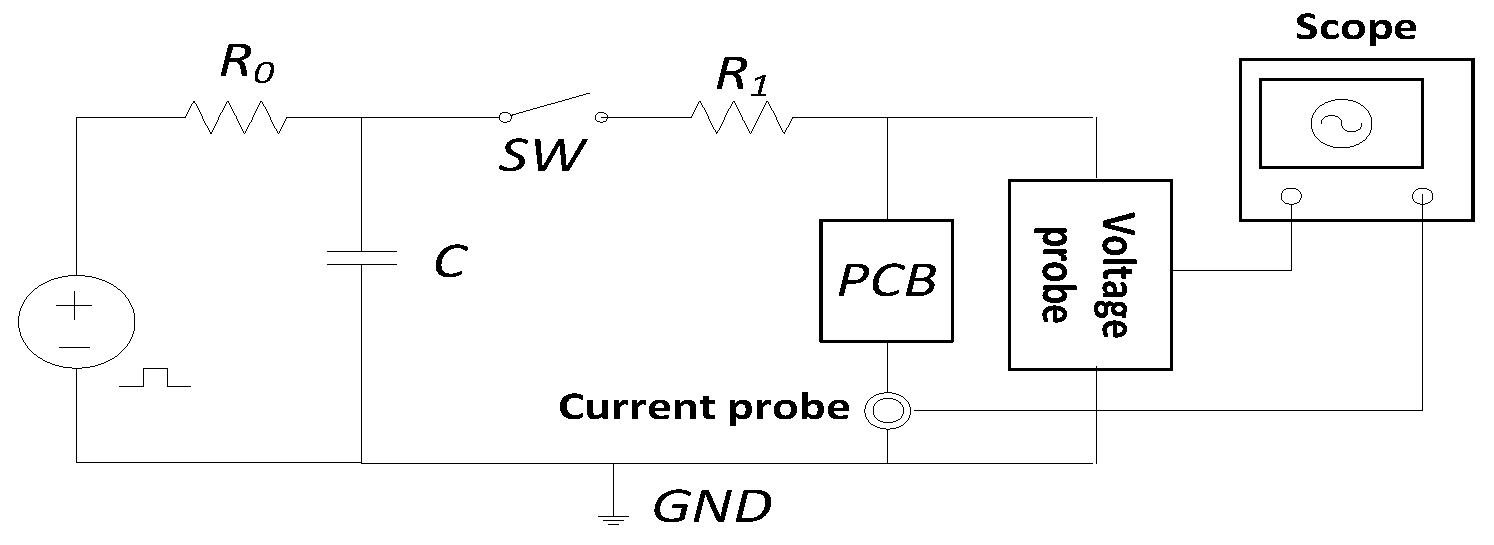
3.1. Experimental System

The test system of the square-wave pulse was composed of a square-wave generator, a power amplifier, a test sample, and a data acquisition and recording system. The schematic of the test system is shown in Figure 4. The square-wave pulse generator generated unipolar square-wave pulse voltage, and the power amplifier improved the output voltage level of the square-wave pulse. An oscilloscope was used to observe the voltage changes at both ends of the electrode and record the breakdown voltage of PCB.
The voltage frequency of the square-wave pulse was set to 1000 Hz, the duty cycle was 60%, the rising and falling times of the edges were set to 200 ns, and the temperature was 15 °C. Figure 5 presents the schematic of the square-wave pulse voltage generated by the test device.
In the picture, T is the period, t1 and t2 are the rising and falling times of the edges, respectively, t/T represents the duty cycle of the square-wave pulse voltage, and Um is the amplitude of the square wave pulse voltage. An experimental system was set up to investigate the insulation characteristics of PCB at different temperatures and pressures. Figure 6 illustrates the model map of the device.

3.2. Experimental Result

The distinguishing influence of factors on the breakdown voltage of the four models was studied through a PCB breakdown test. The voltage amplitude increased gradually at approximately 80 V/s. When breakdown occurred, the voltage amplitude approached 0 V in the oscilloscope. Then, due to the large current after breakdown, the power amplifier automatically sent out an alarm to stop operating. Before this, the voltage applied was the breakdown voltage, which we needed to record.
In the test, a new PCB will be used after recording figure points for different electrode models. However, in the test studying the influence of breakdown times on the breakdown voltage, the same PCB is used to record different breakdown voltages of the test sequence.

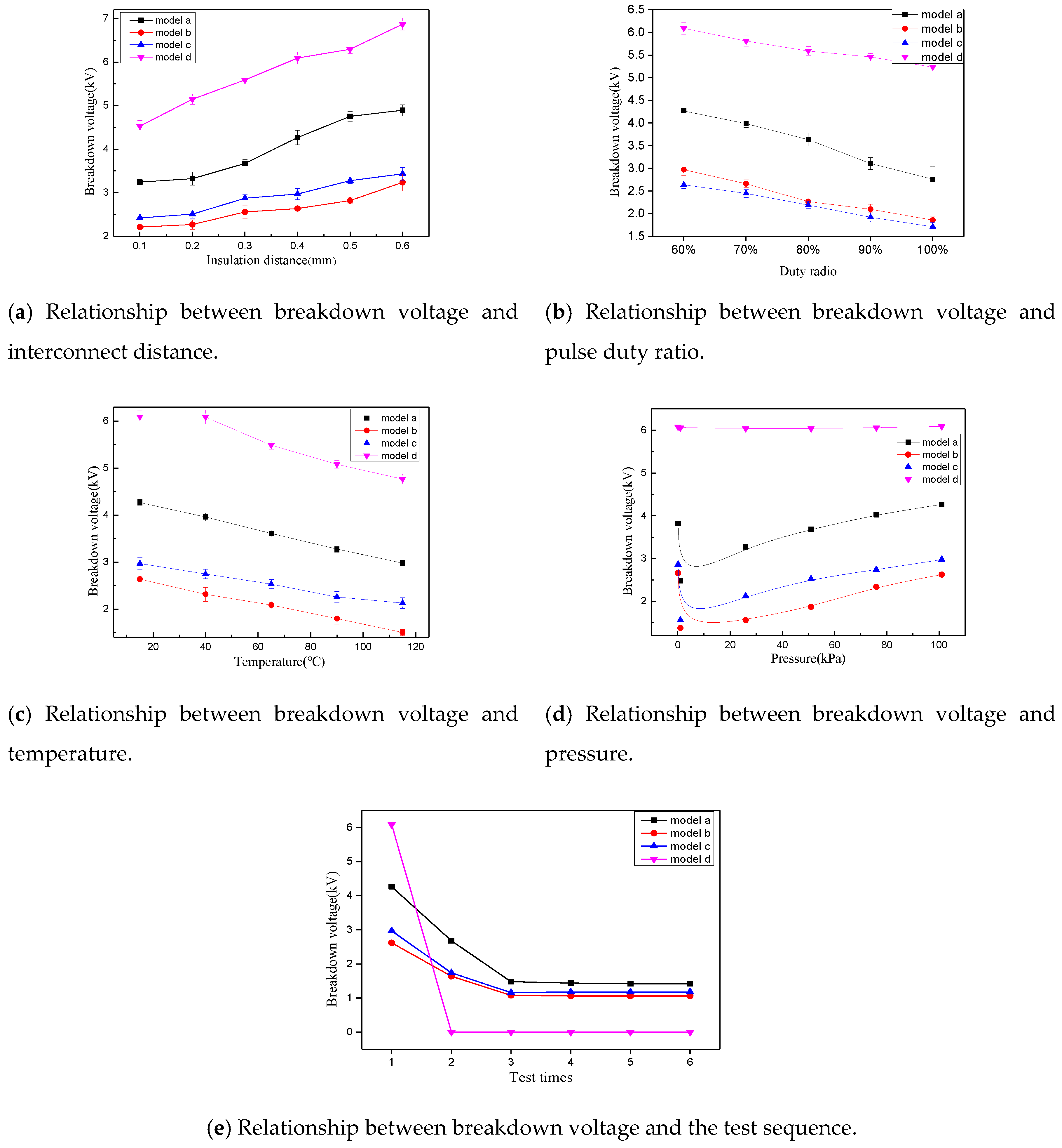
3.2.1. Influence of Interconnect Distance on the Breakdown Voltage of the Four Models

On the basis of extensive experience gained from many previous tests, the square-wave pulse voltage frequency was set to 1000 Hz, the duty cycle was set to 60%, the rising and falling times of edges were set to 200 ns, and the temperature was set to 15 °C to obtain accurate breakdown voltage data. In accordance with the simulation results of the different electric field distributions of the four electrode models, breakdown tests were performed six times on the four models at different insulation distances, and the average value was used as the breakdown voltage in the tests. The experimental results obtained are shown in Figure 7a.

3.2.2. Influence of Pulse Duty Ratio on the Breakdown Voltage of the Four Models

The minimum distance between the four PCB model electrodes (pads) was set to 0.4 mm, and the other test conditions were unchanged. Many previous tests have revealed that when the duty cycle of the square-wave pulse is less than 50%, PCB exhibits obvious partial discharge during the stress-step tests. Consequently, the breakdown voltage is difficult to measure. When the pulse duty is low, the accumulated energy is insufficient to break down the insulating material between the two electrodes, which results in material partial discharge and difficulty in obtaining the breakdown voltage. To obtain accurate breakdown voltage data, we set the duty cycles of the pulse to 60%, 70%, 80%, 90%, and 100% in the tests based on extensive experience gained from experiments. The experimental results obtained are shown in Figure 7b.

3.2.3. Influence of Temperature on the Breakdown Voltage of the Four Models

The PCB electrode model with a gap distance of 0.4 mm was selected as the test object. The duty cycle of the square-wave pulse voltage was set to 60%. Considering the test conditions and glass transition temperature of epoxy resin materials, we set the test temperatures to 15 °C, 40 °C, 65 °C, 90 °C, and 115 °C. Each experiment was repeated six times, and the average value was used as the breakdown voltage under this working condition. The experimental results obtained are shown in Figure 7c.

3.2.4. Influence of Air Pressure on the Breakdown Voltage of the Four Models

Aerospace electronic products must undergo a total pressure change from normal atmospheric pressure to vacuum during the launch process. At normal temperatures, the voltage gap between PCB electrodes remains constant, and the distance between electrodes is 0.4 mm. To study the influence of pressure change on PCB breakdown characteristics, we set the pressures to 0.1, 1, 26, 51, 76, and 101 kPa. The tests were repeated under corresponding air pressures. The average breakdown voltage of six groups of PCBs was adopted as the breakdown voltage of the studied PCB. The experimental results obtained are shown in Figure 7d.

3.2.5. Effect of Breakdown Times on the Breakdown Voltage of the Four Models

Re-breakdown tests were performed on the four electrode models after breakdown to study the influence of breakdown times on the breakdown voltages of the four models. The experimental results obtained are shown in Figure 7d.

3.3. SEM Results

SEM can be used to observe the change in the morphology of insulating polymer media between PCB electrodes on the surface. In this study, the surface morphology of PCB after breakdown was observed by using a Mira3 LMH scanning electron microscope, which is produced by Tescan (Brno, Czech Republic). The formation mechanism of the carbonization channel in the process of PCB breakdown was studied.

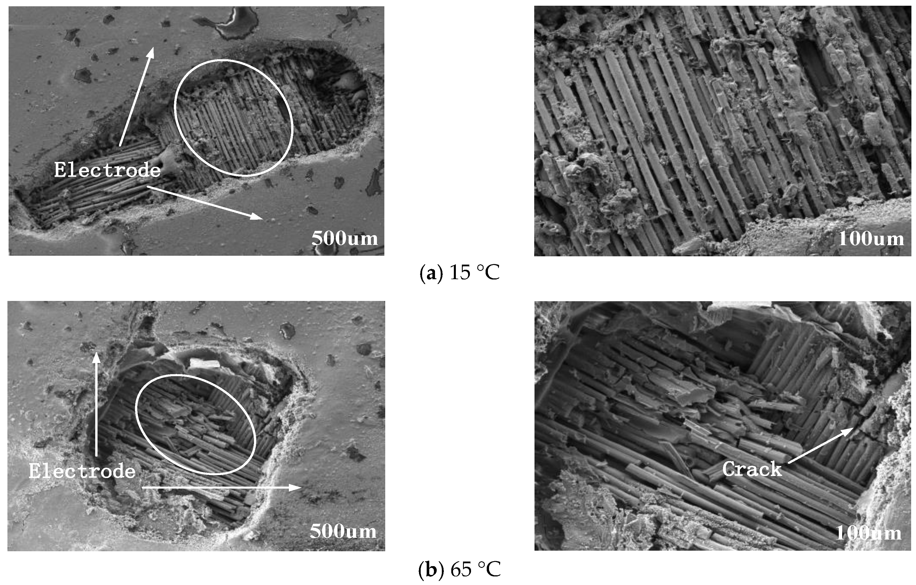
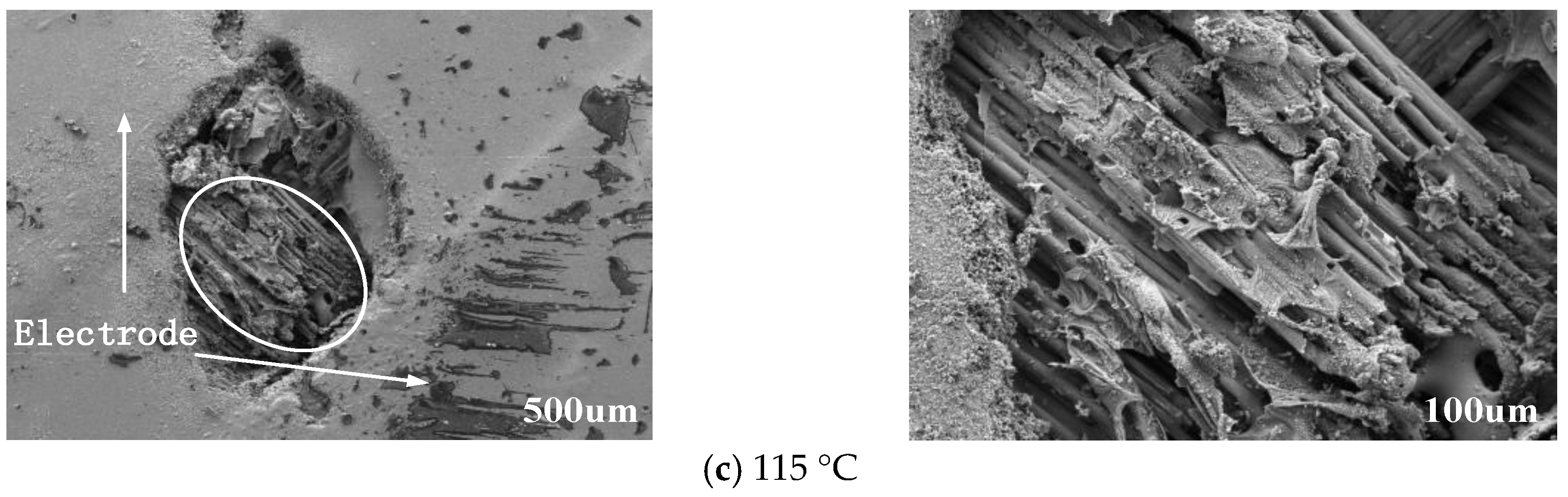
3.3.1. Influence of Temperature on the Breakdown of PCB Insulation

Model (a) was used as the sample for SEM analysis. Models (b) and (c) showed a similar performance and are thus not shown here. Given that the breakdown of Model (d) occurred in the medium, the structure of model (d) was destroyed after dissection. Thus, the scanning electron microscope could observe the carbonization channel of model (d) on the breakdown path. Only model (a) was therefore analyzed. Three PCBs of model (a), which have been subjected to breakdown at 15 °C, 65 °C, and 115 °C, were observed via SEM. The results obtained after scanning are shown in Figure 8.

3.3.2. Influence of Air Pressure on the Breakdown of PCB Insulation

The breakdown carbonization channels of three electrode models at standard and low atmospheric pressures were analyzed through SEM to study the effect of atmospheric pressure on the formation of carbonization channels in the PCB breakdown process. The PCBs of models (a), (b), and (c), which have been subjected to breakdown under 1 and 101 kPa, were observed through SEM. The results are shown in Figure 9.

4. Discussion and Analysis

4.1. Analysis of Experimental Results

The influence of different factors on the breakdown voltages of the four models can be observed clearly from the experimental results shown in the figures. Furthermore, the influence on the breakdown voltages of the four models is distinct.
The general trend of the four models shown in Figure 7a indicates that the change in the breakdown voltage of the four models is consistent with the law that states that breakdown voltage increases with the increase in distance. Among the four models, model (d) had the highest insulation breakdown voltage, and the breakdown voltages of models (b) and (c) were relatively low. According to the simulation analysis, this was caused by the presence of a non-uniform electric field between the two electrodes of models (b) and (c), and a large field intensity distortion was formed at the electrode edge. Meanwhile, the breakdown voltages of models (a), (b), and (c) varied only slightly when the interconnect distance changed from 0.1 mm to 0.2 mm, whereas the breakdown voltage of model (d) increased considerably. The reason is that the insulating medium between the electrodes of model (d) was glass epoxy resin, and the breakdown of model (d) was pure solid breakdown, in which the breakdown voltage increases linearly with the increase in insulation distance. The three other models inevitably adsorbed particles, water, and other impurities on the dielectric surface between two electrodes. As the gap in distance decreased, the impact of impurities on the breakdown process became significant, especially when the gap decreased to a comparable size of the adsorbed impurities. A critical point existed at which the trend of breakdown voltage differed significantly at the scale around the critical point, as shown by the sudden change in breakdown voltage at approximately 0.2 mm in Figure 7a [12].
Figure 7b indicates that the breakdown voltages of the four electrode models decreased with the increase in duty cycle. After the square-wave pulse voltage was applied, the formation of free electrons between PCB electrodes required a certain amount of time. For the air-participated breakdown process (such as models (a), (b), and (c)), the free electrons that appeared between electrodes may have been adsorbed by the gas molecules to form negative ions and may have lost their free ability. However, the formation of free electrons takes time. Given the discontinuity of the unipolar pulse square-wave voltage, the probability of the termination of electron dissociation was reduced when the duty cycle of the pulse voltage increased, which is conducive to the discharge process, thereby reducing the insulation breakdown voltage [13]. For model (d), the chemical reaction between the two electrodes and the formation of carbonization channels required high energy. The increase in duty cycle corresponded to an increase in energy accumulation between the electrodes to a certain extent, which made the carbonization reaction sufficient and further reduced the breakdown voltage [14,15].
In Figure 7c, the change in the breakdown voltage of electrode models (a), (b), and (c) is consistent with the law that states that breakdown voltage decreases with the increase in temperature. However, when the temperature was lower than 65 °C, the breakdown voltage of electrode model (d) did not change obviously with the increase in temperature. During this period, the breakdown of PCB was electrical breakdown, which did not change with the change in temperature. When the temperature exceeded 65 °C, the temperature around the PCB became increasingly high, and the heat dissipation condition worsened. Then, the breakdown of PCB changed from electric breakdown to thermal breakdown, which can explain the change in breakdown voltage in the figure [16,17].
Figure 7d shows that the breakdown voltages of models (a), (b), and (c) decreased initially then increased with the decrease in gas pressure because the breakdown process of these models was surface discharge, which is the breakdown of a “gas–solid composite medium,” and its breakdown process was influenced by gas pressure. When the electrode gap distance was fixed, the relative air density decreased as the pressure decreased from the standard atmospheric pressure. With the increase in the free travel of electrons, the energy of collision accumulation also increased. Although the number of collisions between electrons and gas molecules was reduced, the energy accumulated by electrons was sufficient to cause the gas molecules to dissociate, leading to a decrease in breakdown voltage. When the air pressure was sufficiently low, the relative density of air was very small. Therefore, the number of collisions in electronic motion was greatly reduced. In other words, the probability of molecule dissociation was greatly reduced, so breakdown voltage showed an upward trend in Figure 7d [18,19]. Model (d) experienced pure solid breakdown, and the effect of air pressure on breakdown voltage was unobvious.
As shown in Figure 7e, for electrode model (a), the first breakdown voltage was 4.27 kV. In the second breakdown test, the breakdown voltage dropped to 2.68 kV. The subsequent repeated breakdown tests showed that the breakdown voltage of PCB was basically maintained at approximately 1.48 kV, which indicates that PCB did not completely lose its insulation capacity after breakdown. In other words, the air between the two PCB electrodes also participated in the breakdown process of PCB. Although the solid medium between the two PCB electrodes was broken down, the air between the two electrodes retained a certain insulation capacity. The subsequent breakdown voltage of model (d) was directly reduced to 0 after the first breakdown test. That is, after model breakdown, the solid polymer material between the two electrodes formed a conductive channel, resulting in the loss of insulation capability [20].

4.2. Analysis of SEM Results

The surface morphology of the carbonization channel was observed and analyzed through SEM at breakdowns under different temperatures and pressures, as shown in Figure 8 and Figure 9. The influence of temperature and air pressure on the formation of PCB carbonization channel was also discussed.
Figure 8 shows that the breakdown of PCB that occurred at different temperatures exhibited a great difference in surface morphology. The breakdown depth of the PCB surface was shallow, and the physical structure of the epoxy resin layer under the coating was relatively complete when the ambient temperature was 15 °C. This is because in the process of discharge, the PCB’s ambient temperature was low, and the heat generated in the process of discharge collision was quickly dissipated. Thus, the damage to the physical structure of the PCB’s epoxy layer was small. With the increase in temperature, many fractures in the physical structure of the PCB’s epoxy resin layer was noted on the breakdown channel when the ambient temperature was 65 °C, and the depth of the breakdown channel was much deeper than that at 15 °C. When the ambient temperature was set to 115 °C, nearly all of the epoxy resin layer of PCB was broken near the electrode, and a large amount of scorching material appeared on the epoxy resin layer. This is because a huge amount of heat was produced in the discharge process, and the high external temperature made the accumulated heat difficult to dissipate. As a result, cracking of the polymer between the electrodes occurred fully, resulting in the attachment of many carbides to the surface of the epoxy resin layer. Consequently, the insulation breakdown process of the PCB was accelerated.
Figure 9 indicates that the breakdown of the three electrode models at a low pressure was much smaller than that at the standard atmospheric pressure. The carbonization channel of electrode model (a) was unobvious, except for the change in color, and only the cracks on both sides of the electrode were observed. The carbonization channel of model (b) was striped and distributed along the edge of the electrode, which is consistent with the distribution of the electric field in the simulation. However, the carbonization channel between the two electrodes was located between the two inflexions, and the rest of the electrode was not completely penetrated. This is because the variation in field strength between the two inflection points was serious. Slight physical structure damage of model (c) was observed in the low-pressure carbonization channel, but obvious cracks appeared at the edge of the breakdown channel. The electric field of electrode model (c) was mainly concentrated near the edge of the pad. At a low pressure, the oxygen supply was scarce and the carbon atoms generated between PCB electrodes were difficult to combine with oxygen to produce carbon monoxide and carbon dioxide; thus, most of them remained on the surface of insulating materials. Given carbon’s good conductivity, a complete conductive channel was formed when the two electrodes were completely connected, which resulted in PCB insulation failure. In this process, the impact of electrons destroyed the physical structure of the PCB. However, the heat generated by the electrodes was minimal, so the damage to the physical structure of the electrodes was small.

4.3. Analysis of the Formation of PCB Breakdown Carbonization Channel

The breakage of molecular chains in the carbonization channel observed by SEM showed that a process of electron impact cutting off the molecular chains before PCB breakdown existed. The fracture process of the insulating polymer carbon chain between the PCB electrodes depended not only on the current and heat supply, but also on the impact of electrons during surface discharge.
When air discharge occurred on the PCB surface, the accumulated heat during the discharge process caused carbon deposition on the surface between the two PCB electrodes. Given the high conductivity of carbides, the discharge process between PCB electrodes strengthened further, and many carbides were deposited between the two electrodes. When the carbide between the two electrodes piled up and passed through the two electrodes, a carbonization conduction channel was formed between the two electrodes, which meant that the organic insulating surface between the two PCB electrodes was destroyed. Once the organic insulating surface was destroyed, the insulation properties of the insulating polymer between the PCB electrodes were irreversibly lost. The SEM pictures above show that temperature and pressure had different effects on this process. The voltage type, the electrode type, and the dielectric itself also exerted different effects on the process.

5. Conclusions

An electric field simulation analysis and a breakdown test of four PCB electrode models were performed, and the formation of the PCB breakdown carbonization channel was studied by SEM. The main conclusions are as follows:
(1)
According to the simulation analysis of the electric field, the weakest breakdown point of model (a) was at the junction of the copper foil electrode and the epoxy resin layer, and the electric field intensity between the two conductors presented a U-shaped distribution with symmetry. The weakest breakdown point of model (b) was at the vertex of the corner of the two electrodes. The electrode and pad of model (c) showed field strength distortion, but the distortion at the pad edge was more serious than that at the electrode edge. In model (d), the glass epoxy resin in the vertical area between the two electrodes was the weakest link of PCB insulation, and a large distortion of field strength occurred at the junction between the two electrode edges and the glass epoxy resin.
(2)
The experimental results indicated that the discharge between the single-layer electrodes of the PCB was surface discharge, as observed in models (a), (b), and (c). The breakdown was “gas–solid composite medium”, and the breakdown process was influenced by gas pressure. For models (a), (b), and (c), the breakdown performance of PCBs at different gas pressures was approximately consistent with Paschen’s curve. After the repeated breakdown of these three electrode models, the PCBs of models (a), (b), and(c) still had a certain insulation capacity. In other words, the air between two PCB electrodes also participated in the breakdown process of PCBs, which was of a “gas–solid composite medium”.
(3)
For model (d), the breakdown mode was solid breakdown. An inflection point emerged with the increase in temperature. Before the inflection point, the breakdown voltage was nearly unchanged by the change in temperature. After the inflection point, the breakdown voltage decreased gradually with the increase in temperature. The breakdown voltage of model (d) was almost unaffected by air pressure as well. After breakdown, it basically lost its insulation capacity and was unrecoverable.
(4)
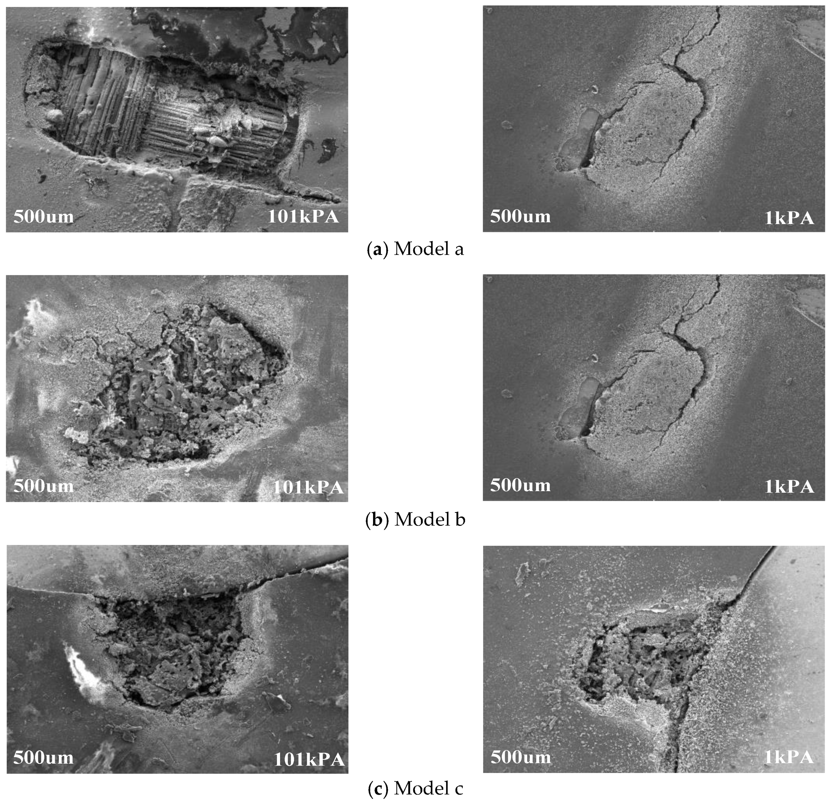
The surface morphology of PCB after breakdown at different temperatures and atmospheric pressures was observed and analyzed through SEM. The position of the breakdown carbonization channel was basically consistent with the position of the simulated insulation weakness, and the two positions could be verified by each other. The results showed that the higher the temperature was, the more serious the damage on the physical structure of the PCB epoxy layer was. The carbonization channel of PCB that was subjected to breakdown at low pressure was lighter than that subjected to breakdown at normal atmospheric pressure, and the damage degree of the PCB insulation structure was small.

Author Contributions

Study concepts were proposed by Q.Z. and M.W. Electrical test, data processing, and the manuscript preparation were done by M.W., T.X. and M.Z. Data analysis and interpretation were done by Q.Z., M.W., M.Z., and L.X. Manuscript editing was performed by T.X., T.J. and X.O.

Funding

This work was supported by National Natural Science Fund of China (51507017).

Acknowledgments

This work was supported by National Natural Science Fund of China (51507017) and Project 111 of the Ministry of Education of China (B08036).

Conflicts of Interest

The authors declare no conflict of interest.

References

  1. Leone, M. Radiated susceptibility on the printed circuit board level: Simulation and measurement. IEEE Trans. Electromagn. Compat. 2005, 47, 471–478. [Google Scholar] [CrossRef]
  2. Tao, J.; Chen, Y. Development of HPM Weapon for Foreign Military. Zhongguo Dianzi Kexue Yanjiuyuan Xuebao (J. China Acad. Electron. Inf. Technol.) 2011, 6, 111–116. [Google Scholar]
  3. Liu, S. Electrostatic Discharge and Harm Protection; Beijing University of Posts and Telecommunications Press: Beijing, China, 2005. [Google Scholar]
  4. Mar, M.H. Electromagnetic Pulse (EMP) Coupling Codes for Use with the Vulnerability/Lethality (V/L) Taxonomy; Technical Report for 45 Military Technology; Weaponry, and National Defense: Adelphi, MD, USA, 1995. [Google Scholar]
  5. Chen, J.; Liu, S.; Tan, Z. Damage Effects of Integrated Circuits Injected by Square Wave Pulse. J. Ordnance Eng. Coll. 2006, 18, 12–15. [Google Scholar]
  6. Chen, J.; Liu, S.; Tan, Z.; He, Q. Similarities and Differences of Damage Effects of Integrated Circuits Injected by ESD Pulse and Rectangular Pulse. High Volt. Eng. 2007, 33, 102–106. [Google Scholar]
  7. Du, B.X.; Gao, Y. Effect of Low Pressure and Magnetic Field on Dielectric Breakdown of Printed Circuit Board. In Proceedings of the International Symposium on Discharges and Electrical Insulation in Vacuum, Matsue, Japan, 25–29 September 2006; pp. 132–135. [Google Scholar]
  8. Moshrefi, T.M.; Swingler, J. Reliability of printed circuit boards containing lead-free solder in aggressive environments. J Mater. Sci. Mater. Electr. 2011, 22, 400–411. [Google Scholar] [CrossRef]
  9. Zhou, Y.; Lan, F. The Effects of Soluble Salts in Dust on Insulation Failure of Printed Circuit Boards. Trans. China Electr. Soc. 2016, 31, 114–119. [Google Scholar]
  10. Meng, G.; Cheng, Y.; Song, J.; Liu, Y.; Wu, K.; Dong, J. Breakdown characteristics of PCB paralleled traces injected by rectangular pulse. In Proceedings of the International Conference on Electrical Insulating Materials, Kyoto, Japan, 6–10 September 2011; pp. 144–147. [Google Scholar]
  11. Zhao, J.; Shen, G. The Design for PCB Land Responding to SMT. Electr. Process Technol. 2002, 23, 192–195. [Google Scholar]
  12. Meng, G.; Cheng, Y.; You, X.; Wu, K.; Liu, Y. Break-down on Interconnect System of Printed Circuit Board under Square Wave Pulse. J. Xian Jiaotong Univ. 2012, 46, 58–63. [Google Scholar]
  13. Li, H.; Yu, D.; Sun, W.; Liu, D.; Li, J. State-of-the-art of Atmospheric Discharge Plasmas. High Volt. Eng. 2016, 42, 3697–3727. [Google Scholar]
  14. Chang, W.; Yan, C.; Bi, J.; Fe, Z. Study on the Relationship between Partial Discharge Development and Electrical Tree Growth in Silicone Rubber. Proc. Csee 2014, 34, 2493–2501. [Google Scholar]
  15. Wang, P.; Wang, J.; Xu, H.; Zhou, K.; Lei, Y.; Zhou, Q. Comparative study of PD characteristics for inverter-fed motor insulation under sinusoidal and repetitive square wave voltage conditions. High Volt. Eng. 2016, 42, 3895–3900. [Google Scholar]
  16. Chao, T. The Breakdown Voltage of Power Transformer Insulation Paper after Thermal Aging. Trans. China Electr. Soc. 2010, 25, 1–8. [Google Scholar]
  17. Liu, T.; Han, S.; Li, Q. Patterns and Development of the Surface Discharge of High Frequency Power Transformer Insu-lation Under Frequency-Dependent Electric Stress. Trans. China Electr. Soc. 2016, 31, 199–207. [Google Scholar]
  18. Gao, W.; Sun, G.; Yan, P. Discussion on the Mechanism of Surface Flashover under High Vacuum. High Volt. Eng. 2005, 31, 1–4. [Google Scholar]
  19. Xue, Y.J.; Yin, X.S. Calculation of Low Pressure Breakdown Threshold of Microwave Devices. Space Electr. Technol. 2012, 12, 55–61. [Google Scholar]
  20. Zhan, H.; Yao, L.; Zhi, L.I.; Duan, S.; Cheng, L.I.; Lin, Z. Research on Repeated Breakdown Process of Disconnector Contact Gap During Very Fast Transient Overvoltage Test of Overall Switching Process of Disconnector in 252 kV GIS. Power Syst. Technol. 2014, 38, 2570–2574. [Google Scholar]
Figure 1. Electrode model of PCB.
Energies 11 02908 g001
Figure 2. 3D simulation model diagram.
Energies 11 02908 g002
Figure 3. Electric field simulation distribution of the four models.
Energies 11 02908 g003
Figure 4. Breakdown test system.
Energies 11 02908 g004
Figure 5. Square-wave pulse.
Energies 11 02908 g005
Figure 6. Model map of the device.
Energies 11 02908 g006
Figure 7. Influence of different factors on the breakdown voltages of the four models.
Energies 11 02908 g007
Figure 8. Surface morphology of the PCB breakdown channel by SEM under different temperatures.
Energies 11 02908 g008aEnergies 11 02908 g008b
Figure 9. Surface morphology of the PCB breakdown channel by SEM under different pressures.
Energies 11 02908 g009
Table 1. Properties of the PCB designed in this study.
CharacteristicUnitTypical Value
Glass Transition Temperature°C132.9/1.3
Volume ResistivityMΩ-cm1.39 × 1010
Surface Resistivity2.25 × 109
Dielectric Constant 4.6
Arc ResistanceS120

