A Novel Phase Current Reconstruction Method for a Three-Level Neutral Point Clamped Inverter (NPCI) with a Neutral Shunt Resistor


Abstract
:1. Introduction
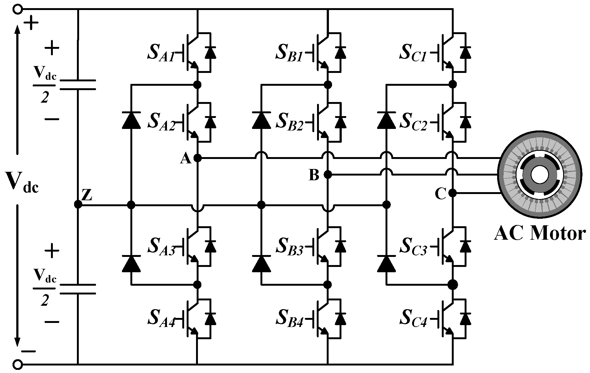
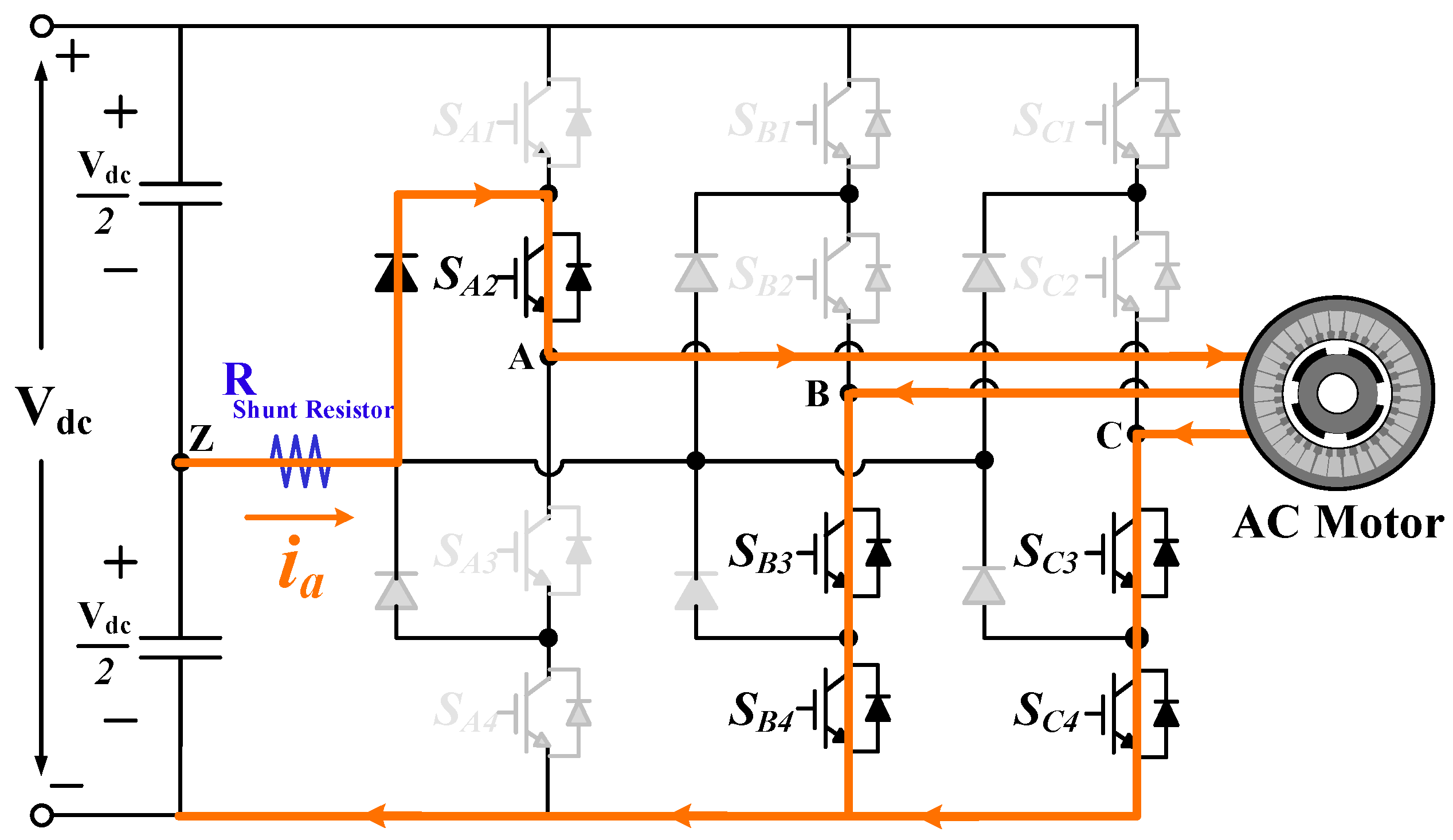
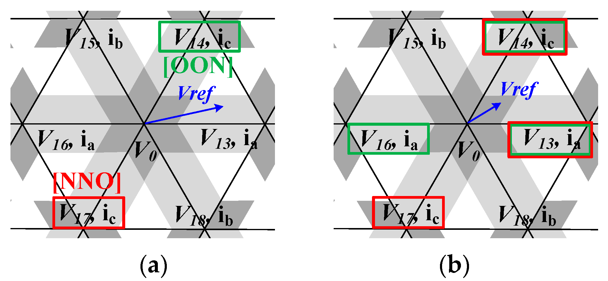
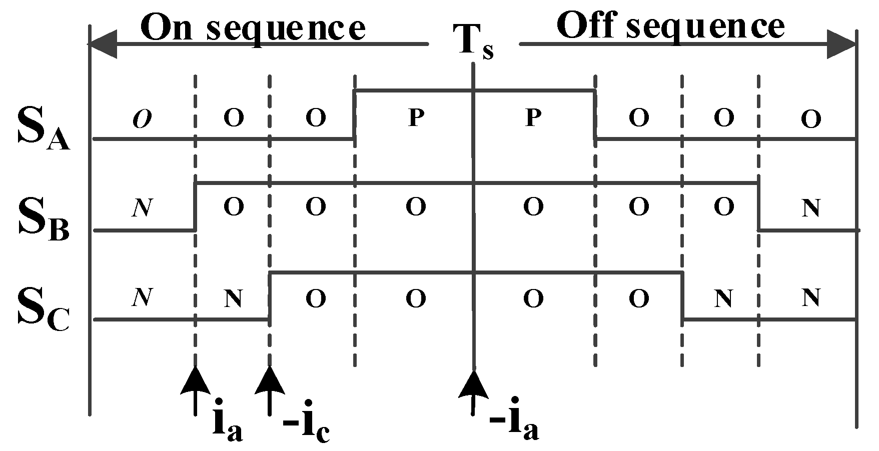
2. Acquiring Phase Current from Neutral Shunt Resistor
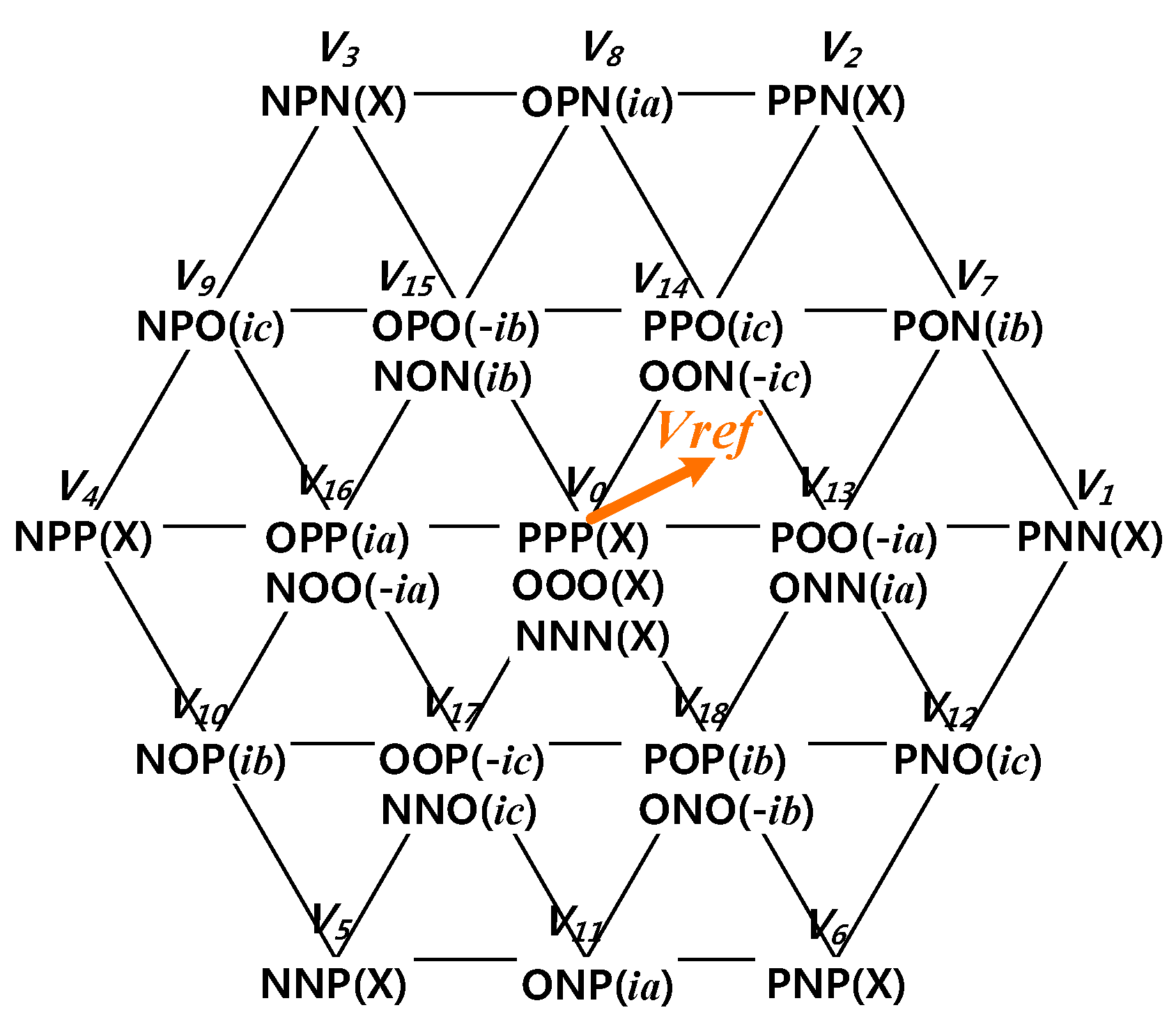
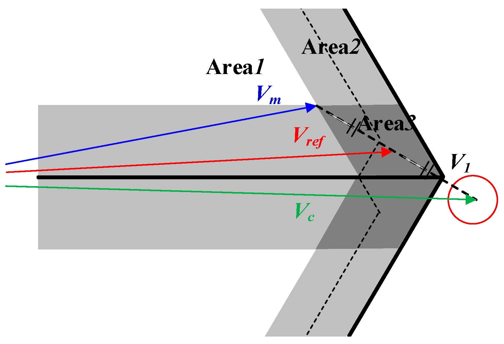
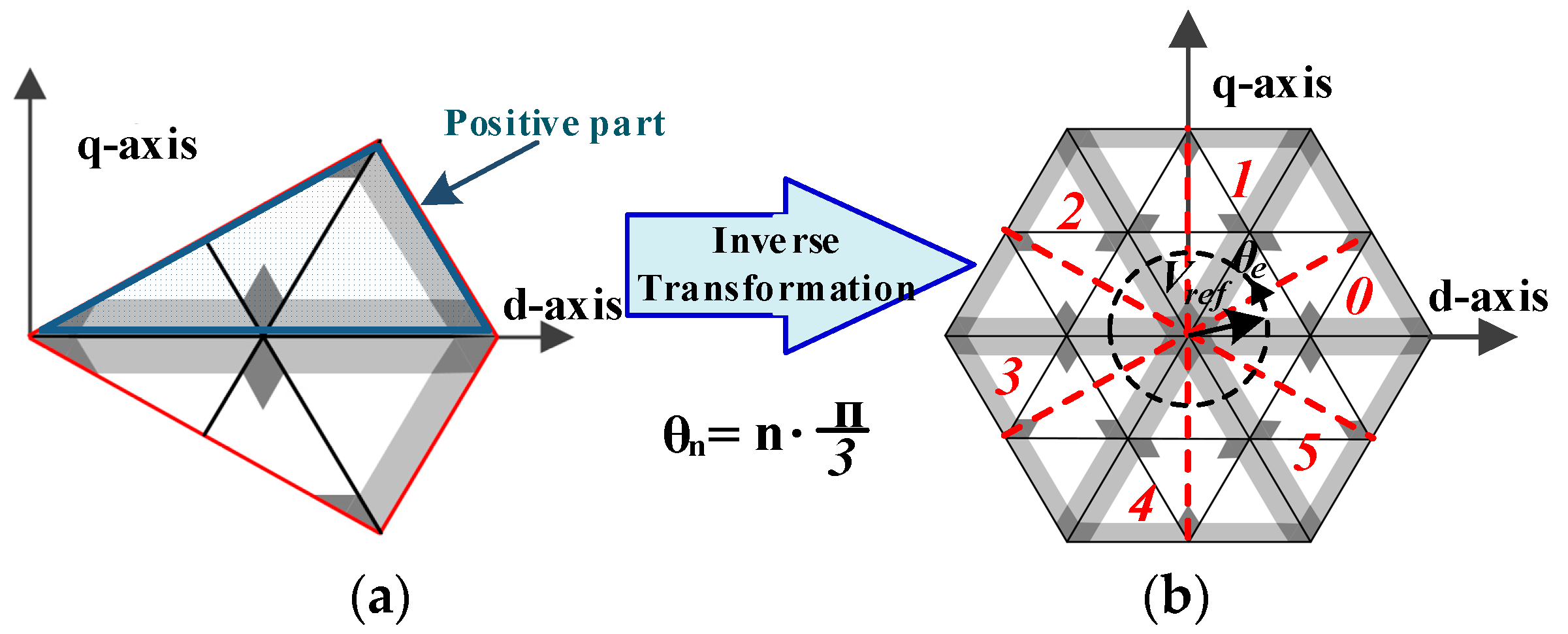
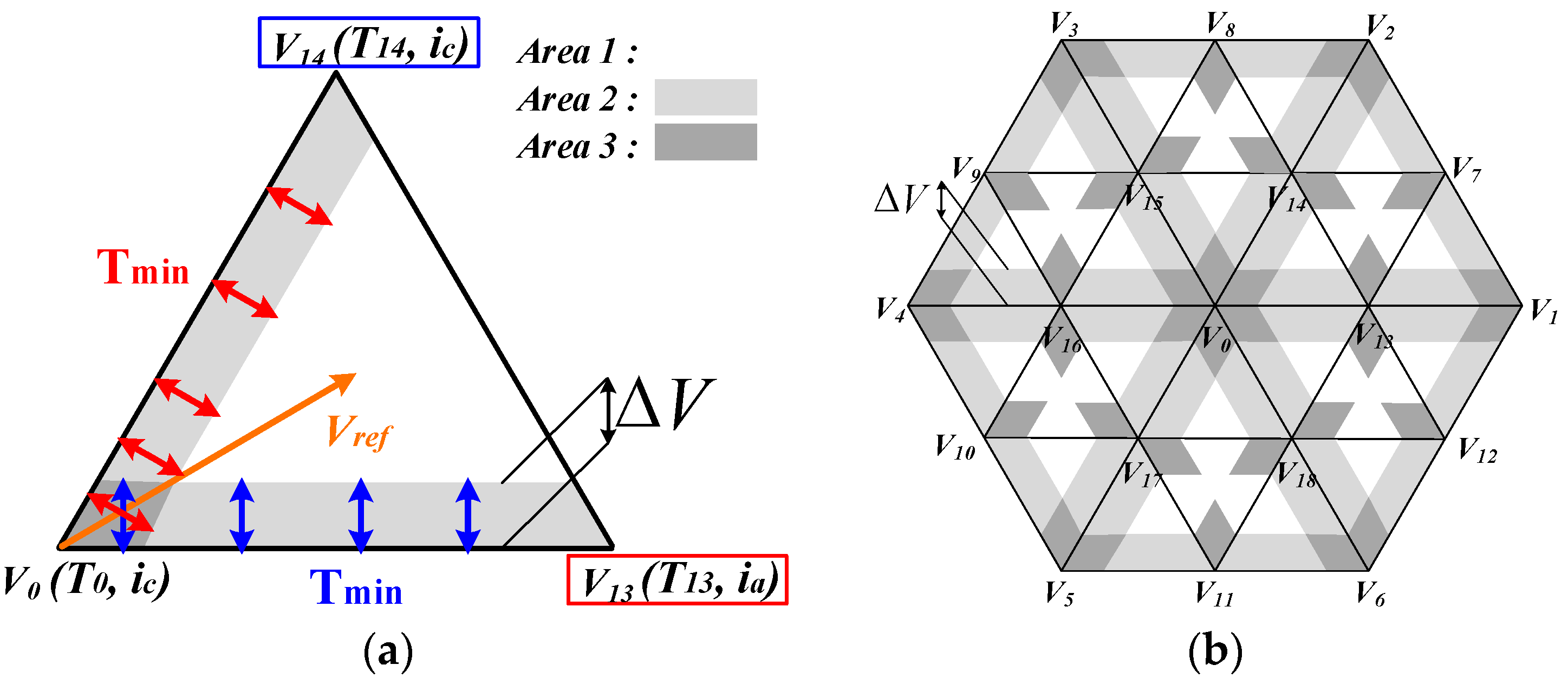
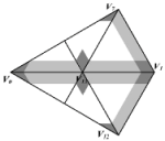
3. Current Unmeasurable Areas
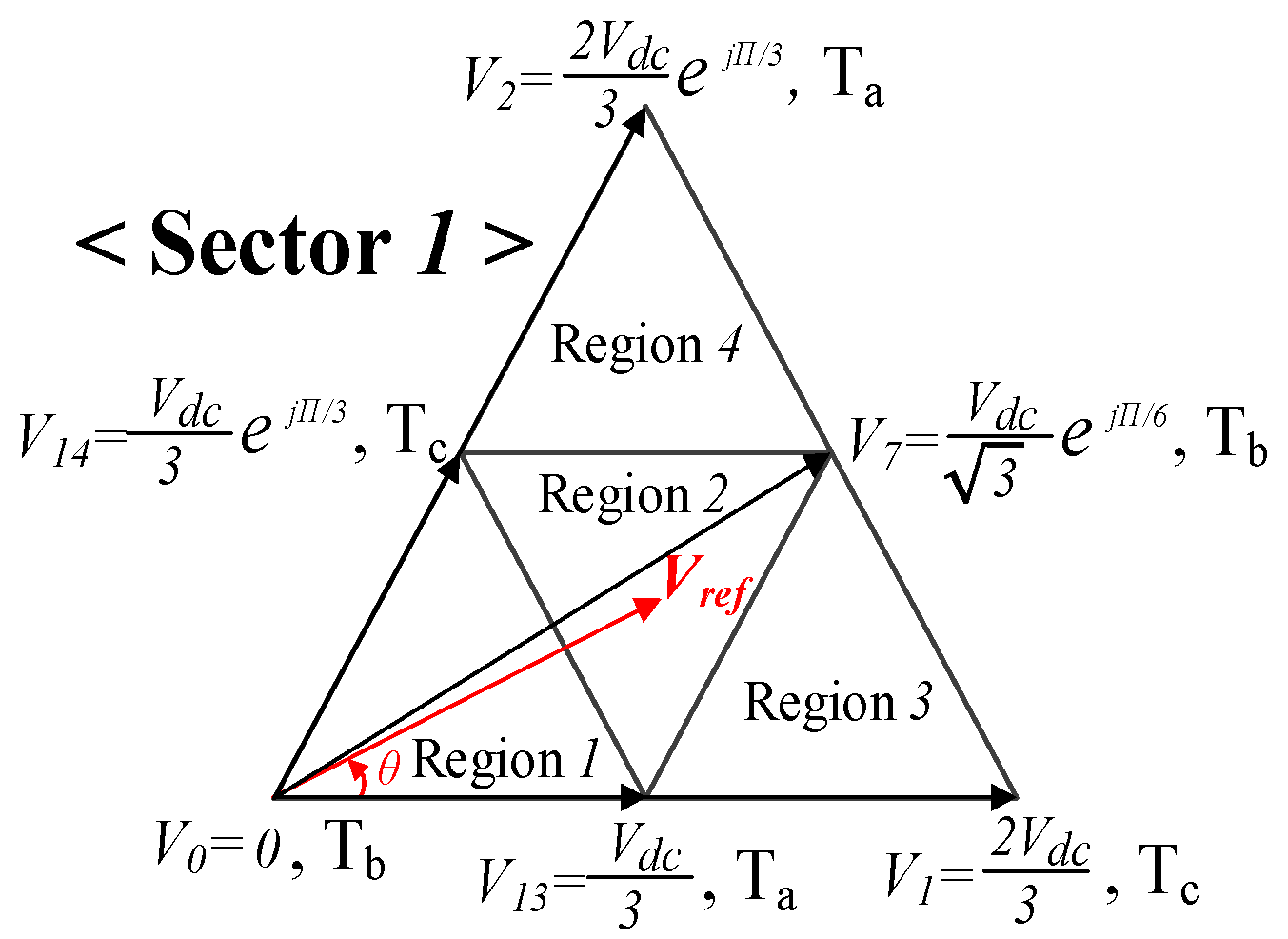
4. Conventional Method of Phase Current Reconstruction
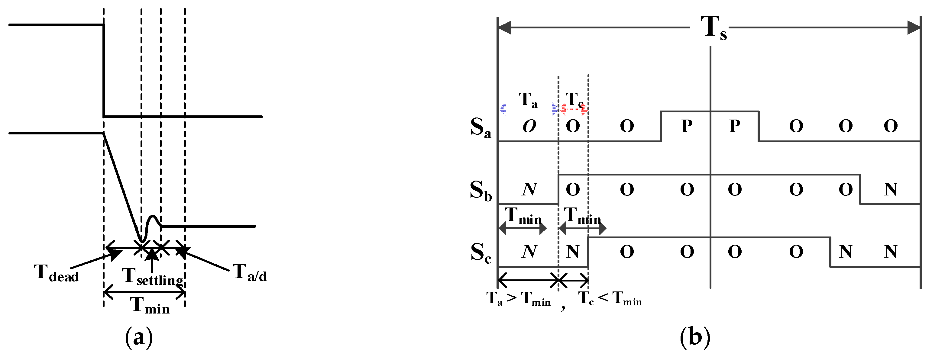
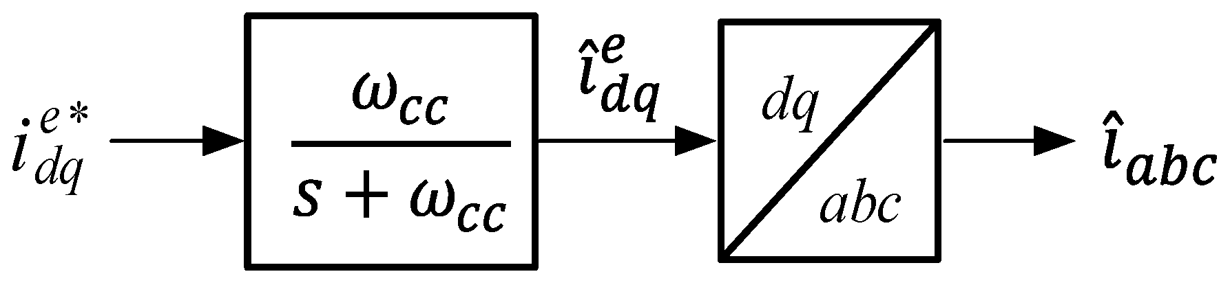
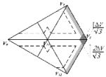
4.1. Modified Voltage Modulation Method
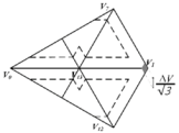
4.2. Minimum Voltage Injection (MVI) Method
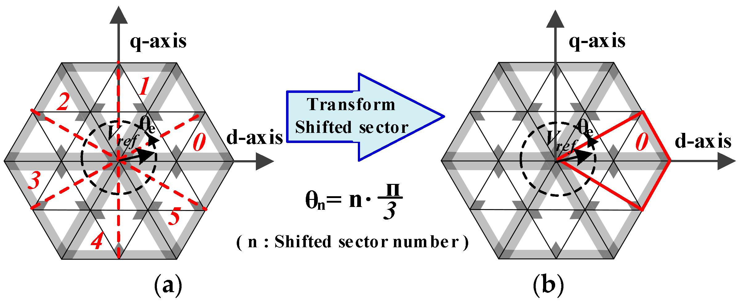
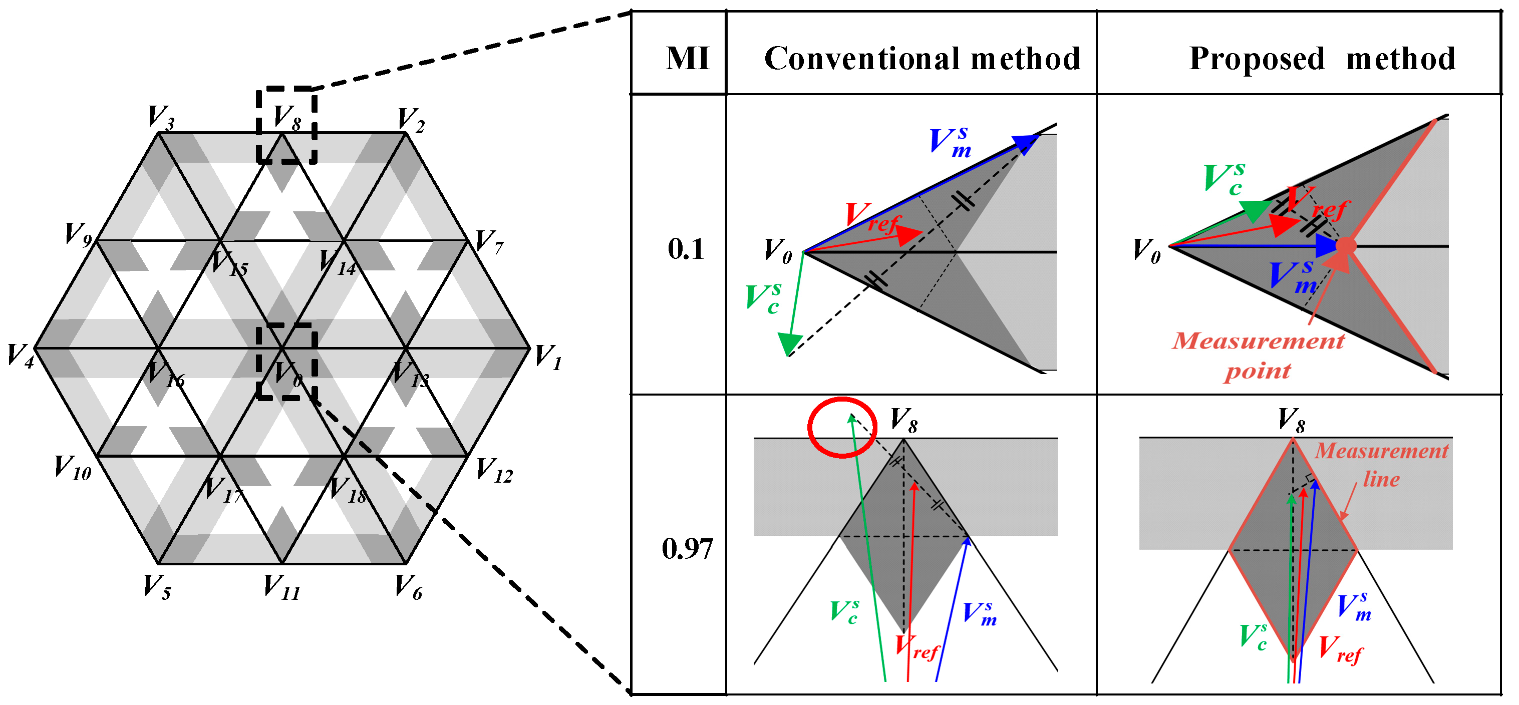
5. Proposed Method of Phase Current Reconstruction
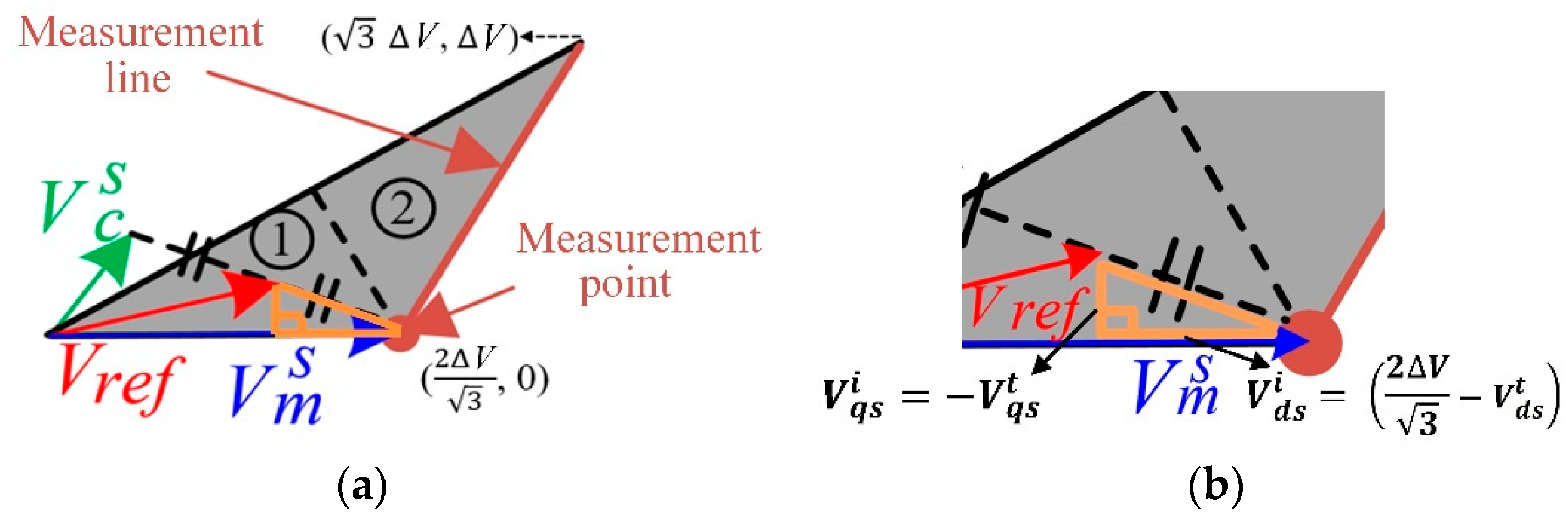
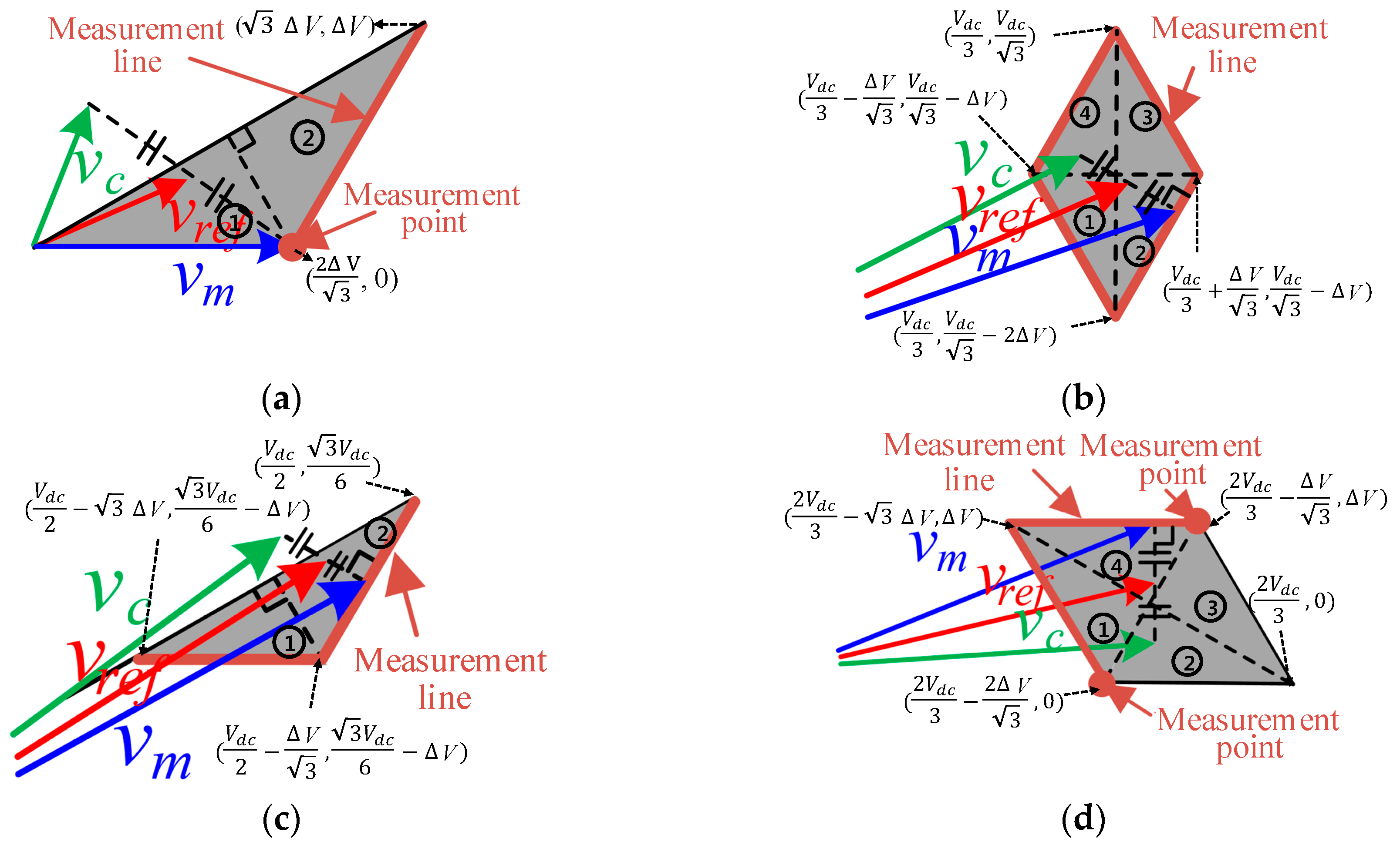
5.1. Based Method for Current Reconstruction in Area 2
5.2. Proposed Method for Current Reconstruction in Area 3
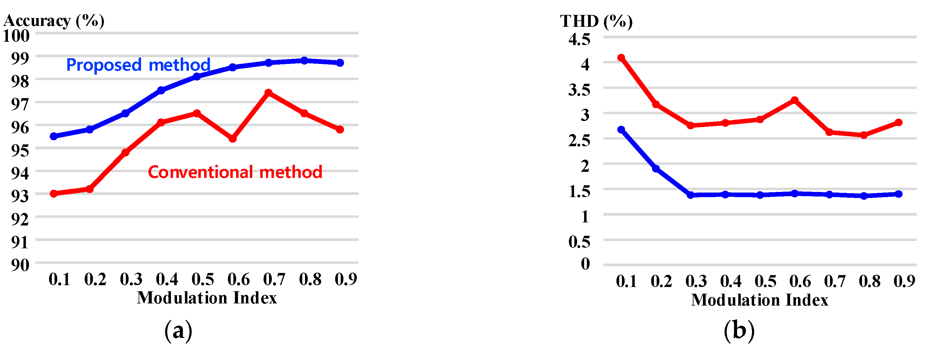
5.3. Comparison of Conventional and Proposed Method
6. Experimental Results
7. Conclusions
Author Contributions
Funding
Acknowledgments
Conflicts of Interest
References
- De, S.; Banerjee, D.; Gopakumar, K.; Ramchand, R.; Patel, C. Multilevel inverters for low-power application. IET Power Electron. 2010, 4, 382–392. [Google Scholar] [CrossRef]
- Lipo, T.A.; Manjrekar, M.D. Hybrid Topology for Multilevel Power Conversion. U.S. Patent 06,005,788, 21 December 1999. [Google Scholar]
- Lai, R.; Wang, F.; Burgos, R.; Pei, Y.; Boroyevich, D.; Wang, B.; Lipo, T.A.; Immanuel, V.D.; Karimi, K.J. A systematic topology evaluation methodology for high-density three-phase PWM AC-AC converters. IEEE Trans. Power Electron. 2008, 23, 2665–2680. [Google Scholar]
- Heldwein, M.L.; Kolar, J.W. Impact of EMC filters on the power density of modern three-phase PWM converters. IEEE Trans. Power Electron. 2009, 24, 1577–1588. [Google Scholar] [CrossRef]
- Jarzebowicz, L. Error Analysis of Calculating Average d-q Current Components using Regular Sampling and Park Transformation in FOC Drives. In Proceedings of the 2014 International Conference and Exposition on Electrical and Power Engineering (EPE 2014), Iasi, Romania, 16–18 October 2014; pp. 901–905. [Google Scholar]
- Shin, H.; Ha, J.I. Phase Current Reconstructions from DC-Link Currents in Three-Phase Three-Level PWM Inverters. IEEE Trans. Power Electron. 2014, 29, 582–593. [Google Scholar] [CrossRef]
- Li, X.; Dusmez, S.; Akin, B.; Rajashekara, K. A New SVPWM for the Phase Current Reconstruction of Three-Phase Three-level T-type Converters. IEEE Trans. Power Electron. 2015, 62, 2627–2637. [Google Scholar]
- Blaabjerg, F.; Pedersen, J.K. An ideal PWM-VSI inverter using only one current sensor in the DC-link. In Proceedings of the 1994 Fifth International Conference on Power Electronics and Variable-Speed Drives, London, UK, 26–28 October 1994; pp. 458–464. [Google Scholar]
- Lee, W.C.; Hyun, D.S.; Lee, T.K. A Novel Control Method for Three-Phase PWM Rectifiers Using a Single Current Sensor. IEEE Trans. Power Electron. 2000, 15, 861–870. [Google Scholar]
- Yeom, H.B.; Ku, H.K.; Kim, J.M. Current reconstruction method for PMSM drive system with a DC link shunt resistor. In Proceedings of the 2016 IEEE Energy Conversion Congress and Exposition (ECCE), Milwaukee, WI, USA, 18–22 September 2016; pp. 18–22. [Google Scholar]
- Ha, J.I. Voltage Injection Method for Three-Phase Current Reconstruction in PWM Inverters Using a Single Sensor. IEEE Trans. Power Electron. 2009, 24, 767–775. [Google Scholar]
- You, J.J.; Jung, J.H.; Park, C.H.; Kim, J.M. Phase current reconstruction of three-level Neutral-Point-Clamped (NPC) inverter with a neutral shunt resistor. In Proceedings of the 2017 IEEE Applied Power Electronics Conference and Exposition (APEC), Tampa, FL, USA, 26–30 March 2017; pp. 2598–2604. [Google Scholar]
- Gu, Y.; Ni, F.; Yang, D.; Liu, H. Switching-State Phase Shift Method for Three-Phase-Current Reconstruction with a Single DC-Link Current Sensor. IEEE Trans. Ind. Electron. 2011, 58, 5186–5194. [Google Scholar]
- Lin, Y.K.; Lai, Y.S. PWM Technique to Extend Current Reconstruction Range and Reduce Common-Mode Voltage for Three-Phase Inverter using DC-link Current Sensor Only. In Proceedings of the 2011 IEEE Energy Conversion Congress and Exposition, 12–16 September 2011; pp. 1978–1985. [Google Scholar]
- Lai, Y.S.; Lin, Y.K.; Chen, C.W. New Hybrid Pulse width Modulation Technique to Reduce Current Distortion and Extend Current Reconstruction Range for a Three-Phase Inverter Using Only DC-link Sensor. IEEE Trans. Power Electron. 2013, 28, 1331–1337. [Google Scholar] [CrossRef]
- Lu, H.; Cheng, X.; Qu, W.; Sheng, S.; Li, Y.; Wang, Z. A Three-Phase Current Reconstruction Technique Using Single DC Current Sensor Based on TSPWM. IEEE Trans. Power Electron. 2014, 29, 1542–1550. [Google Scholar]
- Ying, L.; Ertugrul, N. An Observer-Based Three-Phase Current Reconstruction using DC Link Measurement in PMAC Motors. In Proceedings of the 2006 CES/IEEE 5th International Power Electronics and Motion Control Conference, Shanghai, China, 14–16 August 2006; pp. 1–5. [Google Scholar]
- Saritha, B.; Janakiraman, P.A. Sinusoidal Three-Phase Current Reconstruction and Control Using a DC-Link Current Sensor and a Curve-Fitting Observer. IEEE Trans. Ind. Electron. 2007, 54, 2657–2664. [Google Scholar] [CrossRef]
- Kim, K.; Yeom, H.; Ku, H.; Kim, J. Current reconstruction method with single DC-link. In Proceedings of the 2014 IEEE Energy Conversion Congress and Exposition, 14–18 September 2014; pp. 250–256. [Google Scholar]
- Tomigashi, Y.; Hida, H.; Ueyama, K. Voltage vector correction based on a novel coordinate transformation for motor current detection using a single shunt resistor. In Proceedings of the 2009 13th European Conference on Power Electronics and Applications, 8–10 September 2009; pp. 1–8. [Google Scholar]
- Kim, H.; Jahns, T.M. Integration of the Measurement Vector insertion Method (MVIM) with Discontinuous PWM for Enhanced Single Current Sensor Operation. In Proceedings of the 2006 IEEE Industry Applications Conference Forty-First IAS Annual Meeting, 8–12 October 2006; Volume 5, pp. 2459–2465. [Google Scholar]
- Carpaneto, M.; Marchesoni, M.; Parodi, G. A Sensorless PMSM Drive Operating in the Field Weakening Region Using Only One Current Sensor. In Proceedings of the 2010 IEEE International Symposium on Industrial Electronics (ISIE), 4–7 July 2010; pp. 1199–1204. [Google Scholar]
- Bing, Z.; Du, X.; Sun, J. Control of three-phase PWM rectifiers using a single DC current sensor. IEEE Trans. Power Electron. 2011, 26, 1800–1808. [Google Scholar] [CrossRef]
- Sun, K.; Wei, Q.; Huang, L.; Matsuse, K. An overmodulation method for PWM-inverter-fed IPMSM drive with single current sensor. IEEE Trans. Ind. Electron. 2010, 57, 3395–3404. [Google Scholar] [CrossRef]


| Space Vector | Switching State | Acquiring Current from the Shunt Resistor | Vector Classification | ||
|---|---|---|---|---|---|
| V0 | [PPP], [OOO], [NNN] | X | Zero vector | ||
| P-type | N-type | P-type | N-type | ||
| V13 | [POO] | [ONN] | −ia | ia | Effective vector (Small vector) |
| V14 | [PPO] | [OON] | ic | −ic | |
| V15 | [OPO] | [NON] | −ib | ib | |
| V16 | [OPP] | [NOO] | ia | −ia | |
| V17 | [OOP] | [NNO] | −ic | ic | |
| V18 | [POP] | [ONO] | ib | −ib | |
| V7, V8 | [PON], [OPN] | ib, ia | Effective vector (Medium vector) | ||
| V9, V10 | [NPO], [NOP] | ic, ib | |||
| V11, V12 | [ONP], [PNO] | ia, ic | |||
| V1, V2 | [PNN], [PPN] | X, X | Effective vector (Large vector) | ||
| V3, V4 | [NPN], [NPP] | X, X | |||
| V5, V6 | [NNP], [PNP] | X, X | |||
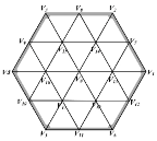
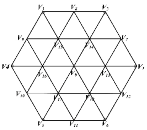
| Region | |||
|---|---|---|---|
| 1 | |||
| 2 | |||
| 3 | |||
| 4 |
| 3-Level NPCI One Shunt Unmeasurable Area | Conventional Method | Proposed Method |
|---|---|---|
 |  |  |
| Unmeasurable area of shifted sector 0 | ||
 |  |  |
| Unmeasurable area of hexagon | ||
© 2018 by the authors. Licensee MDPI, Basel, Switzerland. This article is an open access article distributed under the terms and conditions of the Creative Commons Attribution (CC BY) license (http://creativecommons.org/licenses/by/4.0/).
Share and Cite
Son, Y.; Kim, J. A Novel Phase Current Reconstruction Method for a Three-Level Neutral Point Clamped Inverter (NPCI) with a Neutral Shunt Resistor. Energies 2018, 11, 2616. https://doi.org/10.3390/en11102616
Son Y, Kim J. A Novel Phase Current Reconstruction Method for a Three-Level Neutral Point Clamped Inverter (NPCI) with a Neutral Shunt Resistor. Energies. 2018; 11(10):2616. https://doi.org/10.3390/en11102616
Chicago/Turabian StyleSon, Yungdeug, and Jangmok Kim. 2018. "A Novel Phase Current Reconstruction Method for a Three-Level Neutral Point Clamped Inverter (NPCI) with a Neutral Shunt Resistor" Energies 11, no. 10: 2616. https://doi.org/10.3390/en11102616
APA StyleSon, Y., & Kim, J. (2018). A Novel Phase Current Reconstruction Method for a Three-Level Neutral Point Clamped Inverter (NPCI) with a Neutral Shunt Resistor. Energies, 11(10), 2616. https://doi.org/10.3390/en11102616