Abstract
The use of fuel cells in DC microgrids has been receiving a lot of attention from researchers and industry since both technologies can deliver clean energy with little to no environmental impact. To effectively integrate fuel cells in DC microgrids, a power converter that can equate the fuel cell’s voltage with the DC microgrid’s reference voltage is required. Based on the typical output voltages of fuel cells, buck-boost topologies are commonly used in this type of application. A variety of DC-DC buck-boost topologies, showing distinctive merits and drawbacks, are available in the literature. Therefore, this paper compiles, compares and describes different DC-DC buck-boost topologies that have been introduced in the literature over the past few years. Additionally, some design considerations are addressed, and future work is proposed.
1. Introduction
The European Union has set an ambitious goal for 2050: aiming to become a carbon neutral society, with a more competitive economy, whose growth is fully dissociated from resource use. Working towards this goal will inevitably change the EU’s societal paradigm into a fairer and more prosperous one [1]. The short-term goal, set for 2030, is to reduce greenhouse gas emissions (GGE) by at least 55% [1]. Producing energy through renewable sources is envisioned as a promising way to accomplish this goal. Therefore, support for adoption of renewable energy technologies is expected to grow exponentially [1].
Connecting different renewable energy sources on a single AC grid poses many technical and functional challenges since each source has a different voltage profile and requires different energy conversion stages [2]. A possible way to solve this issue is to use a microgrid, which is smaller, more efficient, and more reliable than a conventional AC grid [2]. This grid operates at a lower DC voltage level than the traditional AC grid and can easily incorporate various renewable sources, such as photo-voltaic (PV) systems, wind turbines or fuel cells (FCs), as well as different energy storage systems, such as batteries, supercapacitors, flywheels and hydrogen storage systems [2]. Furthermore, DC microgrids can either work independently of the main grid, in islanded mode, or connected to it, in grid-connected mode [2].
Nowadays, DC microgrid applications mostly rely on PV technologies. Nevertheless, the use of FCs in microgrids has been studied and researched thoroughly by industry and scholars alike [2]. Unlike other renewables sources, FCs do not depend on external factors such as the wind or the sun. FCs also have a substantially higher power/volume ratio than other renewable sources [3].
Figure 1 depicts an example of a DC microgrid which integrates renewable energy generation supported through FCs, PV panels, and wind turbines.
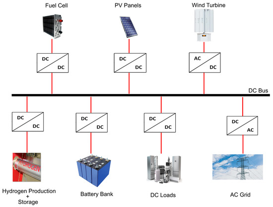
Figure 1.
Example of a DC microgrid’s structure.
The working principle of a FC is based on the conversion of the chemical energy of two reactants, typically hydrogen and oxygen, into electric energy and heat [1,2]. Physically, FCs consist of several single cells connected in series, forming a stack, with a voltage-current profile corresponding to the sum of the individual profiles [2,3]. In turn, a single cell consists of a negative electrode where hydrogen is injected, termed the anode, and a positive electrode where oxygen is injected and water is formed, referred to as the cathode [2]. These electrodes are separated by an electrolyte membrane whose function is to help transport hydrogen protons from the anode to the cathode and prevent electrons from travelling directly between the two electrodes [2].
The blend of these two state-of-the-art technologies, DC microgrids and fuel cells, has already been proven to be practical and promising [3,4,5]. In [4], a comparison between three DC bus voltage levels was conducted to assess which factors impact the overall efficiency of the microgrid. It was concluded that the efficiency of the DC microgrid is strongly dependent on the voltage level, efficiency of the power converter and parasitic ohmic losses [4]. The study also concluded that for lower power applications, such as households, DC microgrids with a 48 V bus voltage were the most suitable for the required power demand [4]. This reference value for DC microgrids was also suggested in [6,7], which reported that it has been widely used for telecommunications applications for a long time and is suitable for low-power household appliances [6]. In addition, power converter technologies are already available on the market since they are used for telecommunications applications in 48 V DC microgrids [7].
Another successful example is presented in [5]. In this work, an integrated energy system, composed of PV panels and FCs, was designed to be implemented in five cities of Mie, Japan. The system operated using the energy provided by the PV panels, with the FCs providing energy to make up for any differences between the demand and the production from the PV panels [5].
The safe and efficient connection of the voltage characteristic of the FC and the reference voltage of its application require the integration of power electronic converters between the FC and the DC microgrid. Different nominal voltages have been provided by FC manufacturers over the past years, with manufacturers aiming to offer even higher voltage levels as the technology progresses [8]. Therefore, when designing a power converter for FC applications in DC microgrids, buck-boost topologies, which can provide lower, equal or higher output voltage levels, are necessary [8]. Buck-boost topologies enable three distinctive operation modes in a single converter: the buck-mode, which happens when the input voltage is higher than the output voltage; the boost-mode, also known as the set-up mode, which occurs when the output voltage is higher than the input voltage; and the third mode, which happens when the input voltage is very similar to the output voltage, hence referred to as the buck-boost mode. Over the years, FCs were mostly employed on electric vehicles. As a result, there is a variety of work concerning FC systems applied to e-mobility solutions [9,10,11,12,13,14]. On the other hand, there is lack of research concerning buck-boost topologies for FC applications in DC microgrids.
Despite all of the benefits associated with adopting power converters, their switching nature introduces ripple, which might affect the FC performance, and thus, the system’s efficiency [15]. The ripple is mostly noted on the current, generating unwanted effects, such as fuel waste and higher losses, low reactant concentration, accelerated electrode aging and decreased FC durability [8,15].
This paper aims to analyse different buck-boost topologies that have been proposed over the past few years, including determining how these topologies can impact FC efficiency. The paper is organised as follows: firstly, a brief introduction on the topic is provided, followed by the description of the coupling behaviour between FCs and power converters; then, different topologies and their merits and demerits are presented; dinally, some conclusions are drawn.
2. Coupling Behavior between FCs and DC-DC Converters
The coupling behaviour between FCs and DC-DC converters was first studied in [16]. In this study, a model aiming at understanding the requirements for the connection between FCs and power converters was developed [16]. It was concluded that, for high frequencies, the electric equivalent model of the FC can be reduced to the internal resistance. Furthermore, the presence of a high capacity at the interface between the electrode and electrolyte, referred to as a double layer capacitor, or CDL, means that the current harmonics are easily filtered by the FC [16]. A scheme of the FC is shown in Figure 2. The study also provided some conclusions on the coupling behaviour between FCs and buck-boost converters. The results showed that the converter input voltage ripple for the boost converter is five times lower than that of the buck converter [16]. Despite the relevant conclusions obtained in [16], the long-term effect of the high current ripple on the CDL was not considered.
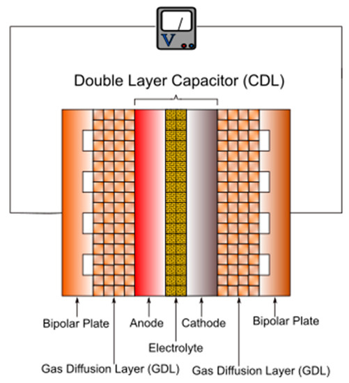
Figure 2.
Fuel cell scheme identifying the CDL.
A similar study was conducted in [17]. The authors verified the use of a FC for heavy-duty vehicles by enhancing the influence of the DC-DC converter’s high switching frequency on the FC’s durability [17]. They discovered that the aging rate of the FC was mostly a consequence of the continuously changing load, whilst for the stationary operation conditions, the voltage decay rate, which is an important metric of degradation, remained constant [17]. Hence, it was concluded that the power converter high switching frequency will not affect the lifetime of the FC as long as it is kept under stationary conditions of operation [17].
Another study analysed the interaction between buck, boost, and buck-boost converters and FCs [18]. The root causes of oscillations in the current and voltage of the FCs and possible mitigation solutions are presented [18]. For the boost converter, the analysis was performed under three different scenarios. All scenarios started with the same load resistance. The first scenario kept the load resistance constant; for scenario number two, a load step was performed, with the resistance being reduced; as for scenario number three, a load step was introduced, with the resistance being increased [18]. Both scenarios one and two showed no significant impact on the oscillation of the FC output. In turn, and due to the low FC output current for scenario three, the same voltage oscillation can no longer be neglected [18]. Therefore, for low current densities on the FC, the boost converter negatively affects the voltage oscillation [18]. The occurrence of these phenomena can be reduced if a capacitor is introduced in between the FC and the boost converter or if the converter switching frequency is increased. This latter option increases the switching losses on the converter [18]. To evaluate the buck converter, two scenarios were considered. For the first scenario, the FC was operated close to the maximum point with a constant duty cycle equal to one [18]. In the second scenario, a load step was introduced such that the FC could operate at a lower power rating [18]. The results showed that for scenario one, no oscillation on the FC voltage was observed since the converter switch was always on, while for scenario two, large oscillations in both FC current and voltage were observed [18]. Such large oscillations increase the fuel consumption and FC temperature. These consequences were not considered in this study. The oscillations can be mitigated if the converter switching frequency is increased or if the FC CDL is increased [18]. This latter technique is implemented by introducing a large capacitor in between the FC and the converter [18].
The coupling behaviour between the FC and the buck converter can be used to estimate the FC parameters, such as the exchange current and the transfer coefficient, by measuring the average inductor current and the amplitude of the FC voltage oscillation. These variables are then considered as inputs for a mathematical model, derived in [18]. Finally, the coupling behaviour between the FC and the buck-boost converter was analysed. The results showed that, due to the presence of a switch in series with the FC output, the buck-boost converter also introduces large oscillations in the FC variables [18].
The literature shows that the current ripple can have a negative effect on the efficiency and overall lifetime of the FC [19]. Therefore, it is necessary to choose a power converter topology capable of eliminating such negative effects by limiting the converter input current ripple, the cost and the number of components, while preserving high efficiency. The next section describes different buck-boost topologies that are suitable for FC applications in DC microgrids, with a focus on the main merits and demerits of each one.
3. Buck-Boost Topologies
The previous section presented the coupling behaviour between the three most basic DC-DC power converter topologies. As mentioned, the buck-boost topology introduces large oscillations in FC voltage and current that ultimately lead to fuel waste and decrease efficiency. The conventional buck-boost topology is shown in Figure 3a. It has a very reduced number of components and the output voltage polarity opposes the input one [20,21]. To solve the oscillation problem, a plethora of different buck-boost topologies have been proposed over the past few years. Although these topologies can be categorised according to the numbers of power switches, some authors also categorise buck-boost converters as current- or voltage-source converters [13].
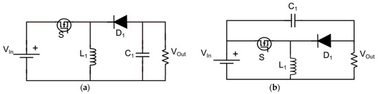
Figure 3.
Conventional buck-boost topology (a). Continuous input current buck-boost converter (CIbB) (b).
A continuous input-current buck-boost (CIbB) DC-DC converter for proton-exchange membrane (PEM) FC applications, which is based on the conventional single-switch buck-boost converter, was introduced in [8]. The converter possesses a capacitor connected in between the positive terminal of the input voltage source and the negative terminal of the load [8]. As illustrated in Figure 3b, this converter is composed of one power switch, one inductor, one diode and two capacitors. The operation principles are quite straightforward. When the power switch is in the ON state, current flows through the inductor to charge it and the capacitor discharges; when the switch is in the OFF state, the capacitor is in charging mode, and the inductor supplies its energy to the load [8]. In the same study, the stability of the converter was also analysed, and a current-mode control was proposed. This control strategy is intended to control the average inductor current; therefore, an input-output feedback linearization technique is required. Furthermore, the versatility of the converter is proven by replacing the diode with a power switch, producing a bidirectional converter. The experimental results showed that both input and output currents are continuous, and that the control algorithm can follow the imposed reference signal [8].
3.1. Ćuk-Based Converters
The Ćuk converter, represented in Figure 4a, is another common buck-boost converter. This converter is used in many different applications, ranging from renewable energies [22,23] to power factor correction [24]. The main merits of this converter are its low output voltage ripple and non-pulsating input and output currents [25]. In contrast, the inverted polarity on the output side is the main drawback. In addition, and due to the presence of just one power switch, this converter shows high component stresses and low conversion efficiency [26]. This converter contains two inductors and two capacitors. This means that it is a high-order power converter with three zeros in the right half plane (RHP), thus making its control quite complex. To solve this problem, authors in [27] obtained its fourth-order transfer function, using state space analysis (SSA), and conducted an order reduction using Padé approximation [27]. They were able to reduce the original two pairs of complex poles in the left half plane (LHP) and the three zeros in the RHP, to just one RHP zero and one pair of complex poles, transforming it into a second-order system [27]. To access the effectiveness of the model order reduction, a step response was performed on both transfer functions. The results showed a good approximation between the two models [27]. To obtain enhanced control capability on the output voltage, a simple compensator was designed using the second-order transfer function [27].
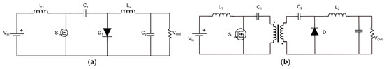
Figure 4.
Ćuk converter (a). Isolated Ćuk converter (b).
The problem of inverse polarity at the converter output can be overcome by means of an isolation transformer [28]. This converter is referred to as an isolated Ćuk converter and has the same advantages as its predecessor. In addition, it also provides electrical isolation between the input and output, as shown in Figure 4b. In [28], the isolated converter was used to interface a pulsed load with a FC. In this application, the load operates at a constant voltage of 8 V, while pulsed current is drawn to the load. The experimental results were performed under an increasing pulsed current and different loads [28]. The results showed that the FC was successfully connected to the pulsed current load. Despite the interesting benefits of the isolated Ćuk converter, some drawbacks should be considered. One drawback is the presence of a transformer, which introduces undesired parasitic losses and limits the available duty cycle range, in both modes of operation (buck or boost). The ratio between the output voltage and input voltage is equal to the inverse of the transformer ratio times the ratio between the power switch in the ON state over the OFF state [29]. Hence, to have equal voltage gain for both buck and boost modes, the ideal transformer turns ratio must be equal to one.
The electrical isolation between the input and output, provided by the isolation transformer, provides the converter with extra security in case of a fault. Like the isolated Ćuk converter, push-pull converters can also be used as buck-boost converters. This converter is based on the forward converter; however, it possesses an extra power switch and a different connection to the intermedium transformer, as depicted in Figure 5a. The additional power switch allows the current to flow continuously through the primary winding of the transformer, as long as the power switches have opposing switching signals [30]. The continuous flowing of current through the primary input of the transformer increases its efficiency and, consequently, the overall converter efficiency. When S1 is ON, a positive voltage is induced in the primary and secondary windings of the transformer. Hence, diode D1 is conducting, and the inductor L1 starts to store energy in the form of a magnetic field. In turn, when S2 is ON, a negative voltage is induced in the primary and secondary windings of the transformer. Therefore, D2 is conducting, while inductor L2 releases its energy. Ideally, there is no delay between the switching signals of the two power switches; nevertheless, due to the microsecond delay in the rise time of physical power switches, for example in MOSFET, such a condition can happen. The negative impact of this condition is a discontinuity of both input and output currents. To avoid this problem, authors in [31] changed the inductor location to the input primary input of the transformer, hence limiting the abrupt change of the input current. The authors also highlighted the importance of overlapping the conduction moments of both power switches, with the aim of safely connecting the inductor. In this configuration, the output capacitor needs to have a reasonably significant capacity. This is because when the switching signals of S1 and S2 are overlapped, no electric and magnetic field is induced in the secondary winding of the transformer due to cancelled flux in the primary winding [31]. Therefore, the load must be temporarily supplied only by the output capacitor [31]. Figure 5b illustrates the proposed converter.
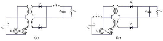
Figure 5.
Buck-boost push-pull converter (a). Current-fed push-pull DC-DC Converter (b).
When compared to the isolated Ćuk converter, the buck-boost push-pull converter shows worse continuity at the input current. The control approach for the push-pull converter is also more complex because the time delay of the power switches must be considered if a non-overlapping strategy is used or if both duty-cycles are greater than 0.5. For the isolated Ćuk, the control approach is much simpler since there is only one power switch. Another distinguishing factor between the two converters is the continuity of the output current. The output current of the isolated Ćuk has significantly lower ripple content when compared to that of the push-pull. Therefore, a more robust output current control can be achieved on the isolated Ćuk converter.
Another Ćuk-based converter was introduced in [32]. This converter not only exhibits similarities with the Ćuk converter, since both have a single power switch, but also possesses similarities with the SEPIC converter, because of the positive voltage output [32]. Both Ćuk and SEPIC converters are limited to a maximum theoretical voltage gain of 10—in practice, such gain is lower due to the converter conduction and switching losses [32]. To solve this issue, while increasing the overall converter efficiency, authors in [32] excluded the hybrid switched-capacitor structure, and added extra passive components, such as inductors, diodes and capacitors. The improved version of the converter, represented in Figure 6a, is composed of a single power switch, four diodes, three inductors and six capacitors (SSBb) [32]. This modification increased the voltage gain by three times and, consequently, the boost range [32]. In the paper, the converter was tested with a 660 W PV system and a 550 W FC operated under different hydrogen supply pressures [32]. The efficiency, defined as the maximum efficiency obtained for a load current of 1 A and the minimum efficiency obtained for a load current of 12 A, was reported to range between 91% to 98%. The authors also suggested a control algorithm based on the theoretical calculation of the duty cycle, which is determined by the desired output voltage and measured input voltage. This algorithm may have difficulties operating under variable loads since there is no feedback from the output voltage. The acquisition of the input voltage may also present a challenge to the effective implementation of the control strategy because it is necessary to suppress all the noise and ripple, which would require a more complex input filter. This drawback could be mitigated if feedback from the output voltage was introduced. Apart from the sensitivity of the controller to perturbations, the main disadvantage of this converter is the pulsating output current, which implies higher capacitance at the converter output.
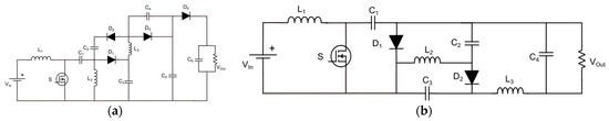
Figure 6.
Single-switch boost-buck converter (SSBb) (a). Ćuk-based single-switch buck-boost converter (CBSS) (b).
Another suitable solution for FC applications was introduced in [33]. The converter (CBSS), presented in Figure 6b, is derived from the Ćuk converter, so it inherits its advantages. In addition, it reduces the inrush currents and the stress imposed on diodes, switches, and capacitors [33]. This converter also has some features of the KY converter, namely the reduced voltage stress on the components. During the OFF state of the power switch, two more modes are added, so the stress on the components is reduced [33]. The voltage gain is two times the one of the Ćuk converter, so there is an increase in the boost range [33]. Despite the considerable advantages of this converter, there are some drawbacks to consider. One of them is the reverse polarity of the output voltage. This feature, inherited from the Ćuk converter, imposes higher voltages across the intermediate capacitors, which increases the risk of short-circuit failure. Therefore, particular attention should be paid to polarity-inverting topologies with regards to capacitor state of health. The adoption of condition monitoring strategies aimed at capacitors could be useful in preventing the short-circuit problem. The high number of passive elements, which potentially increases the parasitic losses, can be considered as another drawback of the converter [33]. Some suggestions for future work include studying the inner dynamics of the converter and applying different control strategies [33].
As already explained, most converters presented so far have at least one zero in the RHP. This is explained by the fact that such converters were derived from the boost converter, which consists of a non-minimum phase system [34]. The literature introduces different solutions to deal with the negative effect of zeros in the RHP. In [35], the proposed technique is based on the inductor current being artificially imposed on the voltage feedback network, thus obtaining the transfer function corresponding to the OFF state of the power converter. Another technique was introduced in [36], where a two-inductor boost converter superimposed with a buck converter solved the RHP problem. For both techniques, complex drivers are required.
A converter suitable for FC applications in DC microgrids was first introduced in [37]. This converter (TSBb), presented in [34], suppresses the effect of the RHP zero by using magnetic coupling inductors and damping networks. The authors were able to mitigate the effect of the RHP through the use of magnetic coupling between the input and output inductors. They were also able to increase the inner dynamics using the damping network, constituted by a capacitor in series with a resistor, which functions as a low-frequency snubber that increases the bandwidth of the proposed converter [37]. The configuration of the converter is based on a cascaded connection between the boost and buck converter, producing a double-switch converter with low components stress and high efficiency, as depicted in Figure 7a [37]. Both conversion stages (buck and boost) possess dedicated inductors that provide non-pulsating currents both in the input and output, low noise level, and some control versability, since it is possible to independently control both the input and output currents [37]. The authors also extracted the transfer function of the converter, concluding that it is a second-order system similar to the buck’s control-to-output transfer function. Therefore, the design of the controller is simplified and it is possible to use well-established control methods [37]. The operation principle is quite simple. For buck mode, the power switch of the buck module is switching, while the boost power switch is kept open. For the boost mode, the buck power switch is kept in the ON state, while the boost module is switching [37]. This converter has already been used in different microgrid applications integrating hybrid energy generation systems. In [38], a FC system hybridised with an auxiliary storage device (ASD) was implemented using the proposed converter. The converter’s control versatility allowed for rapid changes between current control and voltage control depending on the energy level demanded from the microgrid and the ASD [38]. A similar work was reported in [39]. Here, both the FC and ASD act as energy sources, so the microgrid’s voltage does not depend solemnly on the FC [39]. It is necessary to implement more than one converter to properly transfer energy from both input sources to the microgrid [39]. Lastly, a comparative study evaluated different topologies of hybrid systems using FCs and ASDs [40]. The topologies were denominated according to the position of the FC and the ASD: serial hybrid (SH); parallel hybrid (PH) and serial-parallel hybrid (SPH). To compare the three topologies, tests with constant and pulsed loads were performed. The results showed that the SPH topology is more efficient than the other topologies, so it is the topology recommended for applications whose load profile is unknown [40]. Despite the mentioned advantages, the converter presents a problem working in buck-boost mode. This problem is due to the challenging transition between the two operation modes (buck and boost), and it is referred to as the dead zone transition [41]. As described, there are only two operation modes, which can be a disadvantage when the input voltage is very similar to the output voltage. Thus, it is important to guarantee that the converter can either operate in buck, boost or buck-boost mode. To eliminate this challenge, some authors have presented different solutions to mitigate the dead zone. The solutions presented in [42,43] are based on the overlap between buck and boost modes. This method increases the switching losses and only partially solves the discontinuity between the two modes [41]. A more appropriate method was introduced in [44]. In this method, the overlapping concept is preserved, while a maximum threshold is established for the duty cycle applied in buck mode. Later, it was found that the proposed method caused a reduction in the efficiency in buck-boost mode. To solve this problem, the authors that proposed the converter in [37] developed a mitigation algorithm that overlapped the buck and boost modes, while clamping the limits of the duty cycle with a hysteresis window [41]. With this method, it was possible to obtain the three modes of operation and to achieve a smooth transition between buck and boost [41].
Figure 7.
Two-switch boost-buck converter (TSBb) (a). Novel high gain single-switch DC-DC buck-boost converter with continuous input and output power (NISBb) (b).
A more recent Ćuk-based topology (NISBb) was presented in [45]. This converter uses only a single power switch with lower stress, four diodes, four capacitors and three inductors. Unlike its predecessor, this converter has the same output polarity as the input, and the disposition of the capacitors, as illustrated in Figure 7b, provides a significant higher voltage gain when compared to the Ćuk converter. When the power switch is ON the input source provides energy to the inductor L1, while the load is being fed by the capacitors C1, C2 and C3. For the OFF state, the energy stored in the magnetic field of L1 is released to charge the capacitor C1 [45]. At the same time, the energy stored in inductors L2 and L3 is used to charge capacitors C2 and C3 and provide energy to the load [45]. Despite the low stress on the power converter, the gain of the converter does not provide similar ranges for buck and boost mode, which limits its application. Moreover, additional experiments are needed to access the converter’s efficiency.
All in all, Ćuk-based converters are very suitable for FC applications in DC microgrids. Most of the presented converters possess both continuous input and output currents, which helps reduce the negative impact of the current ripple in the FC and allows for enhanced and more accurate current control. The continuity of the input current is possible due to the presence of an inductor in series with the input, meaning that at least one zero will be presen in the RHP. The negative effect of such an inductor can be neglected, or at the bare minimum reduced, if coupled inductors are used. The adoption of a more adaptive approach, based on predictive control could also help. In addition, most Ćuk-based converters only possess one switch, which means that the duty cycle range will be half for the buck mode and half for the boost mode. The third mode, buck-boost, is theoretically obtained when the duty cycle is equal to 0.5. For topologies which possess more than one power switch, such as the TSBb, the duty cycle range is extended.
3.2. Quadratic Converters
The voltage gain of any DC-DC converter is an important factor when choosing the correct topology for a specific application. For applications whose input and output voltage levels are significantly different, the use of isolation transformers, which provide safe integration between input and output, is an interesting solution. Another possible solution consists of the use of quadratic converters. These converters have a quadratic gain, which means that they are suitable for applications whose input and output voltage levels are very different [46,47]. Several high-gain boost DC-DC converters have been presented in the literature. These converters provide a wide input voltage range and have therefore become crucial for FC applications in electrical vehicles [48,49,50]. In [46], a quadratic buck-boost converter with positive polarity at the output voltage and continuous input current (QBBPO) is presented. Both power switches of the converter have the same switching signal, whose duty cycle is the nominal duty cycle of the converter [46]. This converter resembles a cascaded configuration of two traditional single-switch buck-boost converters. To solve the input current continuity problem that is characteristic of the original converter, a group of two capacitors is inserted in parallel in between the input and output. The effective converter operation is strongly dependent on the correct behaviour of the two capacitors that filter the input and output currents. The converter is illustrated in Figure 8a.
Figure 8.
Quadratic buck-boost converter with positive output voltage and continuous input currents (QBBPO) (a). Single-switch quadratic buck-boost with both input and output current continuous converter (SSQBB) (b).
The converter proposed in [47] is a combination between three basic converters: boost, buck-boost and buck converters (SSQBB). Along with the quadratic gain, this converter also has continuous currents at both input and output and possesses a single power switch. Thus, following the cascade sequence, the output voltage of the boost stage is the input of the buck-boost stage, and the output voltage of the buck-boost stage is the input voltage of the buck stage, as shown in Figure 8b. The continuity of the currents is achieved thanks to the inductors from the original circuits of the buck and boost converters. Theoretical analysis showed that the efficiency of the converter increases with the duty cycle, so the converter is more efficient when working on boost mode [47]. The experimental results showed that the higher efficiency was achieved when the voltage gain was higher, resulting in enhanced efficiency for the boost mode. The experimental results also suggested that the dynamics of the converter are satisfied. However, a more thorough analysis of the transfer function aimed at not only understanding the inner dynamics, but also optimising the control strategy, is required. Even though the quadratic gain and the non-pulsating currents are significant advantages of the converter, its practical implementation may be limited by drawbacks such as the reverse polarization of the output voltage and the limited efficiency in buck mode. Other quadratic gain buck-boost topologies were introduced in [51,52]. Despite their reduced number of components when compared to the converter presented in [47], they have pulsating currents at the input, which are unsuitable for FC applications.
Both converters possess the same voltage gain; however, the total number of components is quite different. The QBBPO obtains quadratic gain characteristics without the use of transformers or coupled inductors; rather, it employs the same duty cycle on the power switches. On the contrary, the SSQBB converter uses just one power switch and two storage elements that transfer and store the energy to reach the quadratic voltage gain.
To solve the problem of pulsating currents, a semi-quadratic converter with positive voltage output (SQBuBoC) was introduced in [53].The converter is shown in Figure 9a. It consists of two power switches that are operated simultaneously (as is the converter in [46]), two inductors, two diodes and two capacitors. It has a continuous input current, a wide output voltage range and non-inverting voltage polarity [53]. The low voltage stress across the power switches also improves the converter’s efficiency [53]. When compared with similar converter structures, the efficiency of this converter is higher, thanks to the lower number of components and low voltage stress. The analysis of the transfer function suggests the presence of one zero in the RHP and two in the LHP, as well as two pairs of conjugate poles. The zeros of the system are very suitable to extreme displacement under load variation, meaning that the damping ratio and the settling time will increase for higher output loads [53]. When both output voltage and load are kept constant and there is a change in the input voltage, the effects of the RHP are reduced when the duty cycle is decreasing because the zero is placed far from the origin. On the other hand, when the LHP zeros are closer to the origin, this introduces some instability into the system. To optimize the converter performance, it should operate within the high power range, which implies the adoption of a higher duty cycle [53]. Despite the positive features of the presented converter, some considerations should be made regarding the output current. For applications that require low output current ripple, a capacitor with high capacitance is required, which may lose its filtering effect if placed in parallel with a battery. A similar converter (NOBB), represented in Figure 9b, was introduced in [54]. Both power switches have the same duty cycle, so a semi-quadratic gain is obtained [54]. The input current ripple of this converter is slightly larger in comparison to other semi-quadratic converters because the inductor is not directly placed in series with the input voltage source. Changing the position of the input inductor would improve the filtering capacity of the input current. As expected, the experimental results showed a higher efficiency for the operation in step-up mode. Still, the peak efficiency (around 83%) is low when compared to the other topologies presented previously.
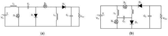
Figure 9.
Transformer-less semi-quadratic buck-boost converter (SQBuBoC) (a). Semi-quadratic negative output buck-boost converter (NOBB) (b).
3.3. Fault-Tolerant DC-DC Converters
To assess the reliability of power electronics converters, a previous study reported on the results of a questionnaire survey which was conducted to determine the main elements of a power converter that are prone to failure in industrial applications [55]. Different semiconductor manufacturers from the aerospace, automation sector and utility power sectors were asked to answer the questionnaire. Questions ranged from power device operating conditions to failure counteraction and costs. The results showed that, within all elements of a power converter, semiconductors, such as IGBTs and MOSFETS, represented 31% of all failures. In contrast, capacitors represented less than 20% of failures, while gate drivers corresponded to 15% of failures [55]. This study clearly shows the importance of semiconductor failures in power converter function.
Although most studies emphasise aspects like reduced components stress, control, and efficiency optimisation, very few fault mitigation strategies have been presented so far. Although it has not been thoroughly addressed, support for the adoption of the interleaving technique to build a fault-tolerant converter structure has been gaining in strength. The interleaving technique is based on connecting multiple layers of the converter in parallel, while shifting the phase by the inverse number of paralleled arms in the converter [8]. This technique helps to reduce the ripple on the input current, and most importantly, assigns fault tolerance to the converter, thus offering extra reliability.
Profiting from the benefits of the interleaving technique, a novel structure of the converter proposed in [8] was derived. This new structure has two arms, so it has twice the components of the original one. Since the current is shifted in each arm, the total current ripple is cancelled, which means that smaller inductors can be used to obtain the desired current ripple [8]. Another topology with a fault tolerance mechanism (FTbbB) is presented in [56]. The authors proposed a fault-tolerant two-stage buck/buck-boost converter with tolerance against open-circuit switch failure that uses redundancy acquired through a synchronous switch for the power switches. The redundant circuit is composed of a single switch and two diodes, hence keeping the number of redundant switches to a bare minimum [56]. The experimental results showed that the control algorithm was able to quickly adapt from the healthy to the faulty state of operation [56]. The converter is represented in Figure 10a.
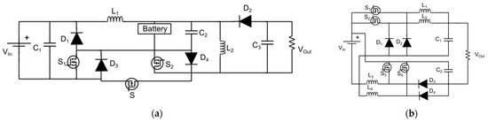
Figure 10.
Fault-tolerant buck/buck-boost converter (FTbbB) (a). Interleaved step-up/step-down converter (ISUSD) (b).
The interleaved technique can be used to reduce the current ripple on the FC. Moreover, this technique can also improve the efficiency and reliability of the converter. For a non-interleaved converter, it is common to increase the switching frequency to reduce component size and the current ripple. However, high switching frequency can cause an increase in the switching losses [57]. To avoid this, one can use the interleaving technique to divide the input power by the multiple arms of the converter [57]. This technique has already been proven to help increase both the efficiency and reliability of the converter [58,59]. One converter that also uses this technique (ISUSD) was proposed in [57]. The proposed technology, illustrated in Figure 10b, consists of a conventional buck module and a floating boost module, where the input terminal of the converter is connected in parallel, while the analogous output terminal is connected in series [57]. Prior to that, each module possesses a two-phase interleaved structure in order to reduce the ripple in the FC current [57]. The working principle of the converter is quite simple: the buck mode is obtained by switching the power switch of that module and keeping the boost’s switch open, while for the boost mode, the buck power switch is kept closed and the boost’s switch is switching [57]. Even though the interleaving technique helped reduce the ripple effect on the FC current, especially for buck mode, the results showed that the input ripple was not satisfactory. This issue can be addressed if additional arms are introduced for the buck module or if the duty cycle is kept below the inverse of the number of arms. To control the input current of the converter, a proportional integral (PI) controller was designed and an average current method was deployed to ensure a smooth transition between the two modes of operation [57].
More recently, a buck-boost topology (4PIBb) was presented in [60]. This topology uses a four-arm interleaved boost converter with changed load connection. In practice, this means that the load is connected in between the cathode of the output diode and the input capacitor, resulting in an inverted output voltage. This configuration, represented in Figure 11, allows for both continuous input and output currents and enables operation in both buck and boost modes, which the traditional boost converter cannot provide. Furthermore, this converter has a relatively low number of components, since the non-interleaved version only requires two capacitors, an inductor, a diode and a power switch. Meanwhile, the interleaved version allows for low input current ripple, which reduces the damage to the FC. To control the input current of the converter, the authors used a current control loop that calculates the duty cycle according to the error between the input current and the reference signal. To ensure a low input ripple, the different PWM signals applied to each converter arm were shifted 90° in sequence with the 0° phase acting as the master control and the following 90°, 180° and 270° as the slave controls. The input current signal was sampled at every turn-on point of the master control signal. The experimental results showed a maximum conversion efficiency of 93% when the converter adopts a constant current, voltage and power control.
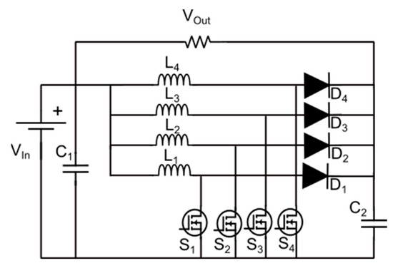
Figure 11.
Four-phase interleaved buck-boost converter (4PIBb).
Table 1 presents a compilation of the main characteristics of each converter such as the number of components, current profile, gain and reported efficiency.

Table 1.
Comparison between the state-of-the-art converter topologies suitable for FC applications.
From the table, it is noted that the total number of components is generally lower for the Ćuk-based converters. This is because these converters only rely on a single switch, larger capacitors and larger inductors. Another notable aspect of the Ćuk-based converters is the relation between the total number of components and the output voltage polarity. Converters such as SSBb, TSBb and NISBb possess a positive output polarity, which means that they have a higher number of components when compared to converters such as CIbB and Ćuk. This translates into a higher efficiency because the stress on the power switch and diodes are lower. In addition, the required inductors and capacitors have lower values than that of other converters. Regarding the quadratic converters, all of them have the same number of components, except for the SSQBB. They are mostly used in applications where the voltage level between input and output are very different. The reported efficiency varies between 60% and 95% for power outputs lower than 100 W. As expected, the fault-tolerant topologies have a higher number of components. This is due to fault-tolerant strategy itself which requires that a finite number of the converter components be in parallel with each other, hence requiring a higher number of components. Moreover, these topologies present a higher efficiency, with values ranging from 91%–95% for power outputs close to 40 kW.
The voltage gain of the Ćuk-based converters, quadratic converters and fault tolerant converters can be easily compared using Figure 12a–c, respectively.
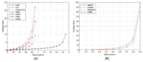
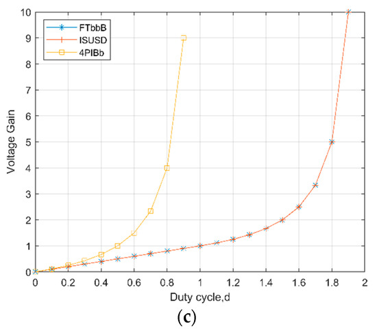
Figure 12.
Cuk-based converters voltage gain (a). Quadratic converters voltage gain (b). Fault-tolerant converters volage gain (c).
In Figure 12a, it is important to notice that for the inverting topologies, the modulus of the voltage gain was considered.. It is also clear that topologies such as CIbB, Ćuk and Isolated Ćuk have the same voltage gain. The TSBb converter shows a lower voltage gain but has a higher range for buck and boost mode than the other converters. Figure 12b shows that quadratic converters have higher voltage gains, albeit at the expense of lower buck ranges, when compared to other converters. Finally, from Figure 12c, it is concluded that the 4PIBb converter has the same voltage gain as most of the Ćuk-based converters, while the other two topologies present a behaviour similar to that of the TSBb converter.
For future work, more robust control approaches, such as the Model Predictive Control (MPC), should be considered. This control method allows for fast and robust responses by predicting the evolution of the control variable, thus increasing the reliability of the overall system. Future work should also aim to improve the converter structure by introducing redundancy to enable fault-tolerant operations. Although some findings addressing this topic were published in [61], the occurrence of faults or how the converter can adapt itself to such faults was not considered.
4. Conclusions
Choosing the right power converter topology for FC systems is a key aspect of the design process because it affects the efficiency and reliability of the overall system. This paper presents a state-of-the-art analysis of different buck-boost topologies which are suitable for FC applications in DC microgrids that have been introduced over the past few years. Intensive research aimed at increasing the efficiency and reliability of both FCs and DC microgrids means that they may provide a safe and clean way for the EU to achieve its goals by 2050. Throughout the paper, the impact of the current ripple was analysed and different topologies were presented and described. Some considerations, such as application, ripple, number of components, voltage level, voltage gain, robustness, cost and efficiency, must be accounted for when choosing the converter. In general, single-switch converters will have a low efficiency and a low number of components, and consequently a reduced cost. Converters such as the Ćuk or the continuous input current buck-boost may be considered for applications where both volume and cost are important factors. Their major drawback is the inverting voltage polarity, which can cause installation problems and undesirable consequences if the components fail. On the other hand, converters with more than one switch tend to have a higher efficiency, but this comes at the expense of a higher number of components and a higher cost. Nevertheless, when considering the entire system, the additional components are responsible for at least a third of the overall efficiency. Some suggestions for future work, especially related to the control approach and fault tolerance, such as using the interleaved technique, MPC methods or both, were also presented.
Author Contributions
Conceptualization, P.A., A.N.A., F.B. and A.J.M.C.; methodology, P.A., F.B., A.N.A. and A.J.M.C.; software, P.A.; validation, P.A.; A.N.A., F.B. and A.J.M.C.; formal analysis, P.A.; investigation, P.A.; resources, A.J.M.C.; data curation, P.A.; writing—original draft preparation, P.A.; writing—review and editing, A.N.A., F.B. and A.J.M.C.; visualization, P.A.; supervision, A.N.A. and A.J.M.C.; project administration, A.J.M.C.; funding acquisition, A.J.M.C. All authors have read and agreed to the published version of the manuscript.
Funding
This work was supported by the Portuguese Foundation for Science and Technology (FCT) under Projects UIDB/04131/2020, UIDP/04131/2020, and 2022.12782.BD.
Institutional Review Board Statement
Not applicable.
Informed Consent Statement
Not applicable.
Data Availability Statement
Not applicable.
Acknowledgments
Not applicable.
Conflicts of Interest
The authors declare no conflict of interest.
References
- Barbir, F. PEM Fuel Cells: Theory and Practice; Elsevier-Academic Press: Amsterdam, The Netherlands, 2005. [Google Scholar]
- Spiegel, C. Designing and Building Fuel Cells; Mcgraw-Hill: New York, NY, USA, 2007. [Google Scholar]
- Li, Z.; Zheng, Z.; Xu, L.; Lu, X. A review of the applications of fuel cells in microgrids: Opportunities and challenges. BMC Energy 2019, 1, 8. [Google Scholar] [CrossRef]
- Alam, M.; Kumar, K.; Srivastava, J.; Dutta, V. A Study on DC Microgrids Voltages based on Photovoltaic and Fuel Cell Power Generators. In Proceedings of the 7th International Conference on Renewable Energy Research and Applications (ICRERA), Paris, France, 14–17 October 2018; Volume 5, pp. 643–648. [Google Scholar] [CrossRef]
- Nishimura, A.; Kitagawa, S.; Hirota, M.; Kolhe, M.L. Energy Assessment of Building Integrated Photovoltaics and Fuel Cell Systems: Design Study for Building(s) of Mie, Japan. Smart Grid Renew. Energy 2017, 08, 129–144. [Google Scholar] [CrossRef][Green Version]
- Li, W.; Mou, X.; Zhou, Y.; Marnay, C. On Voltage Standards for DC Home Microgrids Energized by Distributed Sources. In Proceedings of the 2012 7th International Power Electronics and Motion Control Conference, ECCE Asia, IPEMC, Harbin, China, 2–5 June 2012; Volume 3, pp. 2282–2286. [Google Scholar] [CrossRef]
- Dragičević, T.; Lu, X.; Vasquez, J.C.; Guerrero, J.M. DC Microgrids—Part II: A Review of Power Architectures, Applications, and Standardization Issues. IEEE Trans. Power Electron. 2016, 31, 3528–3549. [Google Scholar] [CrossRef]
- Valdez-Resendiz, J.E.; Sanchez, V.M.; Rosas-Caro, J.C.; Mayo-Maldonado, J.C.; Sierra, J.M.; Barbosa, R. Continuous input-current buck-boost DC-DC converter for PEM fuel cell applications. Int. J. Hydrogen Energy 2017, 42, 30389–30399. [Google Scholar] [CrossRef]
- Chiu, H.J.; Lin, L.W. A bidirectional dc-dc converter for fuel cell electric vehicle driving system. IEEE Trans. Power Electron. 2006, 21, 950–958. [Google Scholar] [CrossRef]
- Kolli, A.; Gaillard, A.; de Bernardinis, A.; Bethoux, O.; Hissel, D.; Khatir, Z. A review on DC/DC converter architectures for power fuel cell applications. Energy Convers. Manag. 2015, 105, 716–730. [Google Scholar] [CrossRef]
- Guilbert, D.; Guarisco, M.; Gaillard, A.; N’Diaye, A.; Djerdir, A. FPGA based fault-tolerant control on an interleaved DC/DC boost converter for fuel cell electric vehicle applications. Int. J. Hydrogen Energy 2015, 40, 15815–15822. [Google Scholar] [CrossRef]
- Wang, H.; Gaillard, A.; Hissel, D. A review of DC/DC converter-based electrochemical impedance spectroscopy for fuel cell electric vehicles. Renew. Energy 2019, 141, 124–138. [Google Scholar] [CrossRef]
- Bhaskar, M.S.; Ramachandaramurthy, V.K.; Padmanaban, S.; Blaabjerg, F.; Ionel, D.M.; Mitolo, M.; Almakhles, D. Survey of DC-DC non-isolated topologies for unidirectional power flow in fuel cell vehicles. IEEE Access 2020, 8, 178130–178166. [Google Scholar] [CrossRef]
- Sreekumar, A.; Jiji, K.S. A Survey of DC-DC Converters for Fuel Cell Electric Vehicle Applications. In Proceedings of the 2021 2nd International Conference for Emerging Technology (INCET), Belagavi, India, 21–23 May 2021; pp. 1–5. [Google Scholar] [CrossRef]
- Ferrero, R.; Marracci, M.; Tellini, B. Impedance spectroscopy on a single PEM fuel cell for the evaluation of current ripple effects. In Proceedings of the 2012 IEEE International Instrumentation and Measurement Technology Conference Proceedings, Graz, Austria, 13–16 May 2012; pp. 52–56. [Google Scholar] [CrossRef]
- Fontes, G.; Turpin, C.; Saisset, R.; Meynard, T.; Astier, S. Interactions Between Fuel Cells and Power Converters: Influence of Current Harmonics on a Fuel Cell Stack. IEEE Trans. Power Electron. 2004, 6, 4729–4735. [Google Scholar] [CrossRef]
- Wahdame, B.; Girardot, L.; Hissel, D.; Harel, F.; Francois, X.; Candusso, D.; Pera, M.C.; Dumercy, L. Impact of power converter current ripple on the durability of a fuel cell stack. In Proceedings of the 2008 IEEE International Symposium on Industrial Electronics, Cambridge, UK, 30 June–2 July 2008; pp. 1495–1500. [Google Scholar] [CrossRef]
- Grötsch, M.; Mangold, M.; Kienle, A. Analysis of the coupling behavior of PEM fuel cells and DC-DC converters. Energies 2009, 2, 71–96. [Google Scholar] [CrossRef]
- Naik, M.V.; Samuel, P. Effect of duty ratio on fuel cell ripple current, power losses and converter efficiency. In Proceedings of the 2017 IEEE PES Asia-Pacific Power and Energy Engineering Conference (APPEEC), Bangalore, India, 8–10 November 2017; Volume 2017, pp. 1–6. [Google Scholar] [CrossRef]
- Ross, J.N.; Kalogirou, S.A. System Electronics, 3rd ed.; Edit. Elsevier Ltd.: Amsterdam, The Netherlands, 2018. [Google Scholar]
- Veerachary, M. Control of Split-inductor Based Buck-Boost Converter. In Proceedings of the 2018 IEEE 8th Power India International Conference (PIICON), Kurukshetra, India, 10–12 December 2018; pp. 6–11. [Google Scholar]
- Xu, W.; Cheng, K.W.E.; Chan, K.W. Application of Cuk converter together with Battery Technologies on the Low Voltage DC supply for Electric Vehicles. In Proceedings of the 2015 6th International Conference on Power Electronics Systems and Applications (PESA), Hong Kong, China, 15–17 December 2015. [Google Scholar] [CrossRef]
- Maroti, P.K.; Padmanaban, S.; Wheeler, P.; Blaabjerg, F.; Rivera, M. Modified High Voltage Conversion Inverting Cuk DC-DC Converter for Renewable Energy Application. In Proceedings of the 2017 IEEE Southern Power Electronics Conference (SPEC), Puerto Varas, Chile, 4–7 December 2017; Volume 2018, pp. 1–5. [Google Scholar] [CrossRef]
- Chen, J.; Maksimović, D.; Erickson, R.W. Analysis and Design of a Low-Stress Buck-Boost Converter in Universal-Input PFC Applications. IEEE Trans. Power Electron. 2006, 21, 320–329. [Google Scholar] [CrossRef]
- Rakshit, S.; Maity, J. Fuzzy Logic Controlled Ćuk Converter. In Proceedings of the 2018 International Conference on Communication and Signal Processing (ICCSP), Chennai, India, 3–5 April 2018; pp. 771–775. [Google Scholar] [CrossRef]
- Restrepo Patiño, C. PEM Fuel Cell Modeling and Converters Design for a 48 V DC Power Bus. PhD Thesis, Departament d’Enginyeria Electrònica, Elèctrica i Automàtica, University of Rovira I Virgili, Tarragona, Spain, 2012. [Google Scholar]
- Kim, E.S.; Kim, C.J.; Kim, Y.T. Controller Design for Cuk Converter Using Model Order Reduction. In Proceedings of the 2012 2nd International Conference on Power, Control and Embedded Systems, Allahabad, India, 17–19 December 2012. [Google Scholar] [CrossRef]
- McGee, B.R.; Nelms, R.M. Using a Cuk Converter to Interface a Pulsed Load to a Fuel Cell. In Proceedings of the Intersociety Energy Conversion Engineering Conference, Washington, DC, USA, 29–31 July 2002; pp. 313–318. [Google Scholar] [CrossRef]
- Khan, H.R.; Kazmi, M.; Ashraf, H.B.; Khalid, M.H.B.; Hasan, A.; Qazi, S.A. An isolated power factor corrected cuk converter with integrated magnetics for brushless dc ceiling fan applications. Electronics 2021, 10, 1720. [Google Scholar] [CrossRef]
- Ivanovic, Z.; Knezic, M. Modeling Push–Pull Converter for Efficiency Improvement. Electronics 2022, 11, 2713. [Google Scholar] [CrossRef]
- Maiti, D.; Mondal, N. Design procedure of a push pull current-fed dc-dc converter. In Proceedings of the National Power Electronics Conference (NPEC-2010), Uttarakhand, India, 10–13 June 2010; pp. 1–7. [Google Scholar]
- Dhimish, M.; Schofield, N. Single-switch boost-buck DC-DC converter for industrial fuel cell and photovoltaics applications. Int. J. Hydrogen Energy 2022, 47, 1241–1255. [Google Scholar] [CrossRef]
- Ajami, A.; Ardi, H.; Farakhor, A. Design, analysis and implementation of a buck-boost DC/DC converter. IET Power Electron. 2014, 7, 2902–2913. [Google Scholar] [CrossRef]
- Calvente, J.; Martinez-Salamero, L.; Valderrama, H.; Vidal-Idiarte, E. Using magnetic coupling to eliminate right half-plane zeros in boost converters. IEEE Power Electron. Lett. 2004, 2, 58–62. [Google Scholar] [CrossRef]
- Paduvalli, V.V.; Taylor, R.J.; Hunt, L.R.; Balsara, P.T. Mitigation of Positive Zero Effect on Nonminimum Phase Boost DC-DC Converters in CCM. IEEE Trans. Ind. Electron. 2018, 65, 4125–4134. [Google Scholar] [CrossRef]
- Mourra, O.; Fernandez, A.; Tonicello, F. Buck boost regulator (B2R) for spacecraft solar array power conversion. In Proceedings of the 2010 Twenty-Fifth Annual IEEE Applied Power Electronics Conference and Exposition (APEC), Palm Springs, CA, USA, 21–25 February 2010; pp. 1313–1319. [Google Scholar] [CrossRef]
- Restrepo, C.; Calvente, J.; Cid-Pastor, A.; el Aroudi, A.; Giral, R. A Noninverting Buck–Boost DC–DC Switching Converter With High Efficiency and Wide Bandwidth. IEEE Trans. Power Electron. 2011, 26, 2490–2503. [Google Scholar] [CrossRef]
- Ramirez-Murillo, H.; Restrepo, C.; Calvente, J.; Romero, A.; Giral, R. Energy management DC system based on current-controlled buck-boost modules. IEEE Trans. Smart Grid 2014, 5, 2644–2653. [Google Scholar] [CrossRef]
- Ramírez-Murillo, H.; Restrepo, C.; Calvente, J.; Romero, A.; Giral, R. Energy Management of a Fuel-Cell Serial-Parallel Hybrid System. IEEE Trans. Ind. Electron. 2015, 62, 5227–5235. [Google Scholar] [CrossRef]
- Ramirez-Murillo, H.; Restrepo, C.; Konjedic, T.; Calvente, J.; Romero, A.; Baier, C.R.; Giral, R. An Efficiency Comparison of Fuel-Cell Hybrid Systems Based on the Versatile Buck-Boost Converter. IEEE Trans. Power Electron. 2018, 33, 1237–1246. [Google Scholar] [CrossRef]
- Restrepo, C.; Konjedic, T.; Calvente, J.; Giral, R. Hysteretic Transition Method for Avoiding the Dead-Zone Effect and Subharmonics in a Noninverting Buck–Boost Converter. IEEE Trans. Power Electron. 2015, 30, 3418–3430. [Google Scholar] [CrossRef]
- Wei, C.L.; Chen, C.H.; Wu, K.C.; Ko, I.T. Design of an Average-Current-Mode Noninverting Buck–Boost DC–DC Converter With Reduced Switching and Conduction Losses. IEEE Trans. Power Electron. 2012, 27, 4934–4943. [Google Scholar] [CrossRef]
- Lee, Y.J.; Khaligh, A.; Emadi, A. A Compensation Technique for Smooth Transitions in a Noninverting Buck–Boost Converter. IEEE Trans. Power Electron. 2009, 24, 1002–1015. [Google Scholar] [CrossRef]
- Paul, R.; Maksimovic, D. Analysis of PWM Nonlinearity in Non-Inverting Buck-Boost Power Converters. In Proceedings of the 2008 IEEE Power Electronics Specialists Conference, Rhodes, Greece, 15–19 June 2008; Volume 3, pp. 3741–3747. [Google Scholar]
- Hosseini, S.H.; Ghazi, R.; Movahhed, S.K. A Novel High Gain Single-Switch DC-DC Buck-Boost Converter with Continuous Input and Output Power. In Proceedings of the 2019 24th Electrical Power Distribution Conference (EPDC), Khoramabad, Iran, 19–20 June 2019; pp. 10–15. [Google Scholar] [CrossRef]
- Rosas-Caro, J.C.; Sanchez, V.M.; Valdez-Resendiz, J.E.; Mayo-Maldonado, J.C.; Beltran-Carbajal, F.; Valderrabano-Gonzalez, A. Quadratic buck-boost converter with positive output-voltage and continuous input-current. In Proceedings of the 2018 28th International Conference on Electronics, Communications and Computers (CONIELECOMP), Cholula, Mexico, 21–23 February 2018; Volume 2018, pp. 152–158. [Google Scholar] [CrossRef]
- Zhang, N.; Zhang, G.; See, K.W.; Zhang, B. A single-switch quadratic buck-boost converter with continuous input port current and continuous output port current. IEEE Trans. Power Electron. 2018, 33, 4157–4166. [Google Scholar] [CrossRef]
- Mustafa, A.; Mekhilef, S. Dual Phase LLC Resonant Converter with Variable Frequency Zero Circulating Current Phase-Shift Modulation for Wide Input Voltage Range Applications. IEEE Trans. Power Electron. 2021, 36, 2793–2807. [Google Scholar] [CrossRef]
- Ahmad, J.; Siddique, M.D.; Sarwar, A.; Lin, C.H.; Iqbal, A. A high gain noninverting DC–DC converter with low voltage stress for industrial applications. Int. J. Circuit Theory Appl. 2021, 49, 4212–4230. [Google Scholar] [CrossRef]
- Khan, S.; Zaid, M.; Siddique, M.D.; Iqbal, A. Ultra high gain step up DC/DC converter based on switched inductor and improved voltage lift technique for high-voltage applications. IET Power Electron. 2022, 15, 932–952. [Google Scholar] [CrossRef]
- Miao, S.; Wang, F.; Ma, X. A New Transformerless Buck-Boost Converter with Positive Output Voltage. IEEE Trans. Ind. Electron. 2016, 63, 2965–2975. [Google Scholar] [CrossRef]
- Mostaan, A.; Gorji, S.A.; Soltani, M.N.; Ektesabi, M. A novel single switch transformerless quadratic DC/DC buck-boost converter. In Proceedings of the 2017 19th European Conference on Power Electronics and Applications (EPE’17 ECCE Europe), Warsaw, Poland, 11–14 September 2017; Volume 2017, pp. P1–P6. [Google Scholar] [CrossRef]
- Hasanpour, S.; Mostaan, A.; Baghramian, A.; Mojallali, H. Analysis, modeling, and implementation of a new transformerless semi-quadratic Buck–boost DC/DC converter. Int. J. Circuit Theory Appl. 2019, 47, 862–883. [Google Scholar] [CrossRef]
- Ding, S.; Wang, F. A New Negative Output Buck-Boost Converter with Wide Conversion Ratio. IEEE Trans. Ind. Electron. 2017, 64, 9322–9333. [Google Scholar] [CrossRef]
- Yang, S.; Bryant, A.; Mawby, P.; Xiang, D.; Ran, L.; Tavner, P. An industry-based survey of reliability in power electronic converters. IEEE Trans. Ind. Appl. 2011, 47, 1441–1451. [Google Scholar] [CrossRef]
- Siouane, S.; Jovanovic, S.; Poure, P. Open-switch fault-tolerant operation of a two-stage buck/buck-boost converter with redundant synchronous switch for PV systems. IEEE Trans. Ind. Electron. 2019, 66, 3938–3947. [Google Scholar] [CrossRef]
- Gao, D.; Jin, Z.; Liu, J.; Ouyang, M. An interleaved step-up/step-down converter for fuel cell vehicle applications. Int. J. Hydrogen Energy 2016, 41, 22422–22432. [Google Scholar] [CrossRef]
- Kolluri, S.; Narasamma, N.L. Analysis, modeling, design and implementation of average current mode control for interleaved boost converter. In Proceedings of the 2013 IEEE 10th International Conference on Power Electronics and Drive Systems (PEDS), Kitakyushu, Japan, 22–25 April 2013; pp. 280–285. [Google Scholar] [CrossRef]
- Khosroshahi, A.; Abapour, M.; Sabahi, M. Reliability evaluation of conventional and interleaved DC-DC boost converters. IEEE Trans. Power Electron. 2015, 30, 5821–5828. [Google Scholar] [CrossRef]
- Wang, D.; Wang, Z.; Peng, Z.; Zhang, Y.; Cheng, X.F. A Four-Phase Interleaved Buck-Boost Converter with Changed Load Connection for the Fuel Cell Activation. IEEE Access 2021, 9, 102104–102113. [Google Scholar] [CrossRef]
- Samavatian, V.; Radan, A. A novel low-ripple interleaved buck-boost converter with high efficiency and low oscillation for fuel-cell applications. Int. J. Electr. Power Energy Syst. 2014, 63, 446–454. [Google Scholar] [CrossRef]


Publisher’s Note: MDPI stays neutral with regard to jurisdictional claims in published maps and institutional affiliations. |
© 2022 by the authors. Licensee MDPI, Basel, Switzerland. This article is an open access article distributed under the terms and conditions of the Creative Commons Attribution (CC BY) license (https://creativecommons.org/licenses/by/4.0/).