Article

A 12-b Subranging SAR ADC Using Detect-and-Skip Switching and Mismatch Calibration for Biopotential Sensing Applications

Information and Communication System-on-Chip (SoC) Research Center, School of Electronics and Information, Kyung Hee University, Yongin 17104, Korea
*
Author to whom correspondence should be addressed.
Sensors 2022, 22(9), 3600; https://doi.org/10.3390/s22093600
Submission received: 11 April 2022 / Revised: 3 May 2022 / Accepted: 8 May 2022 / Published: 9 May 2022
(This article belongs to the Section Biosensors)

Abstract

:
This paper presents a 12-b successive approximation register (SAR) analog-to-digital converter (ADC) for biopotential sensing applications. To reduce the digital-to-analog converter (DAC) switching energy of the high-resolution ADC, we combine merged-capacitor-switching (MCS) and detect-and-skip (DAS) methods, successfully embedded in the subranging structure. The proposed method saves 96.7% of switching energy compared to the conventional method. Without an extra burden on the realization of the calibration circuit, we achieve mismatch calibration by reusing the on-chip DAC. The mismatch data are processed in the digital domain to compensate for the nonlinearity caused by the DAC mismatch. The ADC is realized using a 0.18 μm CMOS process with a core area of 0.7 mm2. At the sampling rate fS = 9 kS/s, the ADC achieves a signal-to-noise ratio and distortion (SINAD) of 67.4 dB. The proposed calibration technique improves the spurious-free dynamic range (SFDR) by 7.2 dB, resulting in 73.5 dB. At an increased fS = 200 kS/s, the ADC achieves a SINAD of 65.9 dB and an SFDR of 68.8 dB with a figure-of-merit (FoM) of 13.2 fJ/conversion-step.

1. Introduction

Portable biomedical sensing applications demand low-power consumption for long battery operation. The human biopotentials have low-frequency bandwidth, up to a few kHz [1]. The amplitude of an electrocardiogram (ECG) is around 1 mV. An electroencephalogram (EEG) has an amplitude from 10 to 100 µV over a frequency band from 0.5 Hz to 150 Hz. The local field potential (LFP) has a typical amplitude of 1 mV over 1 Hz to 200 Hz. The biopotentials are low-amplitude signals, which must be amplified before signal processing. The next important block for signal processing will be the analog-to-digital converter (ADC). Thus, the performance of the amplifier and ADC determines the quality of the measured biopotentials. For digitizing the amplified signal, successive approximation register (SAR) ADC is suitable, with its energy-efficient structure for medium resolution. Moreover, the scaling-friendly structure of the SAR ADC has drawn continued research interest [2]. The basic building blocks of the SAR ADC include a comparator, a digital-to-analog converter (DAC), and SAR logic. The power consumption of the SAR logic, which is mostly digital, can be reduced by lowering the supply voltage. The comparator power can be reduced using a dynamic structure. Thus, researchers have investigated various energy-efficient DAC switching methods—for example, split-DAC [3], monotonic switching [4], set and down [5], and energy saving [6]. The work in [7] introduces a merged-capacitor-switching (MCS) method. In this approach, DAC capacitors are switched from the common-mode (CM) voltage VCM to ground or reference voltage VREF. This method not only saves switching energy but also effectively handles the issues related to CM variations. Behavioral simulation of a 10-bit SAR ADC shows 93.4% less switching energy than the conventional method.
A high-resolution SAR ADC demands a relatively large DAC area and switching energy. Switching energy is usually dominant in the capacitors of the most significant bit (MSB) segment rather than those in the least significant bit (LSB) segment. The work in [8] achieves efficient DAC switching using detect-and-skip (DAS). This approach allows skipping capacitor switching in the MSB segment, still generating the correct residue for the DAC. Implemented in 40 nm CMOS, the 10-bit SAR ADC achieves a signal-to-noise ratio and distortion (SINAD) of 55.6 dB and a spurious-free dynamic range (SFDR) of 76.2 dB; however, this work uses a split capacitor for the DAC, which is suboptimal in terms of energy efficiency compared to the MCS. If we can combine the merits of DAS and MCS, this approach can further reduce the DAC switching energy. Moreover, the work in [8] does not support DAC calibration; therefore, it cannot handle the mismatch caused by the parasitics and process variations.
Several approaches investigate techniques for DAC mismatch calibration. The work in [9] presents an on-chip dual calibration method for comparator offset and DAC mismatch. The work in [10] presents an energy-efficient ADC using digital domain calibration without additional analog circuits. The work in [11] presents a 13-bit SAR ADC with on-chip calibration for capacitor error compensation. Implemented in 130 nm CMOS, the ADC achieves a SINAD of 66.3 dB and an SFDR of 71 dB by consuming 1.47 μW; this approach suffers from a relatively large area of 0.9 mm2. A digital calibration method is presented using a sub-radix-2 redundant architecture [12], which can handle dynamic errors in the conversion process. The work in [13] analyzes the characteristics of the nonbinary-weighted capacitive DAC and a bottom-up weight calibration technique; however, these works have the drawback of altering the full-scale weight, which is different from the ideal value.
In this work, we present a 12-bit subranging SAR ADC suitable for low-power biopotential sensing applications. We reduce the DAC switching energy by combining MCS and DAS methods, successfully embedded in the subranging structure. Behavioral simulation of a 12-bit SAR ADC shows that the proposed method reduces 96.7% of switching energy compared to the conventional method, which is up to 9.2% lower than the previous state-of-the-art [7]. Without an extra burden on the realization of the on-chip calibration circuit, we implement digital domain calibration to compensate for the nonlinearity caused by the DAC mismatch. To address the drawback of the previous approach altering the weight of the full scale, we adopt a normalized full-scale weight for the subranging ADC. Using the proposed calibration technique, the ADC fabricated in 0.18 μm CMOS demonstrates successful operation and performance improvement. At a sampling rate of 200 kS/s, the ADC achieves a SINAD of 65.9 dB with a figure-of-merit (FoM) of 13.2 fJ/conversion-step. An SFDR of 68.8 dB is achieved near the Nyquist frequency. The novelty of this work is efficiently combining MCS and DAS for a high-resolution ADC and implementing a digital domain calibration using a normalized full-scale weight for the subranging ADC.

2. Design

2.1. Subranging SAR ADC

Figure 1a shows the proposed subranging ADC. It includes a 7-bit coarse SAR ADC, a 12-bit fine SAR ADC, a DAS controller, a calibration (CAL) logic, and an output buffer. The coarse ADC includes the DAC consisting of seven binary-weighted capacitors CCk (k = 1 to 7). The fine ADC includes the DAC designed with twelve binary-weighted capacitors. For mismatch calibration, we divide the DAC into a 7-bit MSB segment of capacitors Ci (i = 6 to 12) and a 5-bit LSB segment of capacitor Cj (j = 1 to 5). MCS is used for coarse and fine ADCs to save DAC switching energy.
The analog input is sampled into the two ADCs at the same time. Top-plate sampling is performed using a bootstrapped switch operating with 1.8 V [9]. After sampling the input, the coarse ADC sequentially generates 7-bit output DOUT,C[12:6]. Then, the DAS controller and fine ADC are enabled by the signal CDONE (coarse done). The DAS controller decodes DOUT,C[12:6], and sets the switches for Ci (i = 6 to 12) of the fine ADC. This operation generates the residue in the fine DAC. Then, the SAR logic of the fine ADC sequentially determines the switch states of the remaining Cj (j = 1 to 5) to generate DOUT,F[5:1]. The DOUT,C[12:6] and DOUT,F[5:1] are combined in the output buffer to generate the ADC output DOUT[12:1] with the end-of-conversion (EOC) signal.
Figure 1b shows the timing sequence for the subranging ADC, which consists of calibration and conversion modes. The calibration mode includes three steps: reset, mismatch measurement, and data loading. When the reset signal becomes high, calibration mode starts with the calibration-enabled signal CAL. In this mode, the DAC inputs are disconnected from the analog input. During this time, the calibration code DCAL[6:1] for Ci (i = 6 to 12) is generated and loaded two times (positive and negative DAC). Two bootstrap switches are used to set the bottom plate of the DAC capacitor to VCM. These switches are controlled by the output CALp,n of the CAL logic at the beginning of each calibration cycle. The data loading occurs at the falling edge of EOC_CAL (end of calibration), which captures DCAL[6:1]. After finishing the calibration, the ADC enters conversion mode.
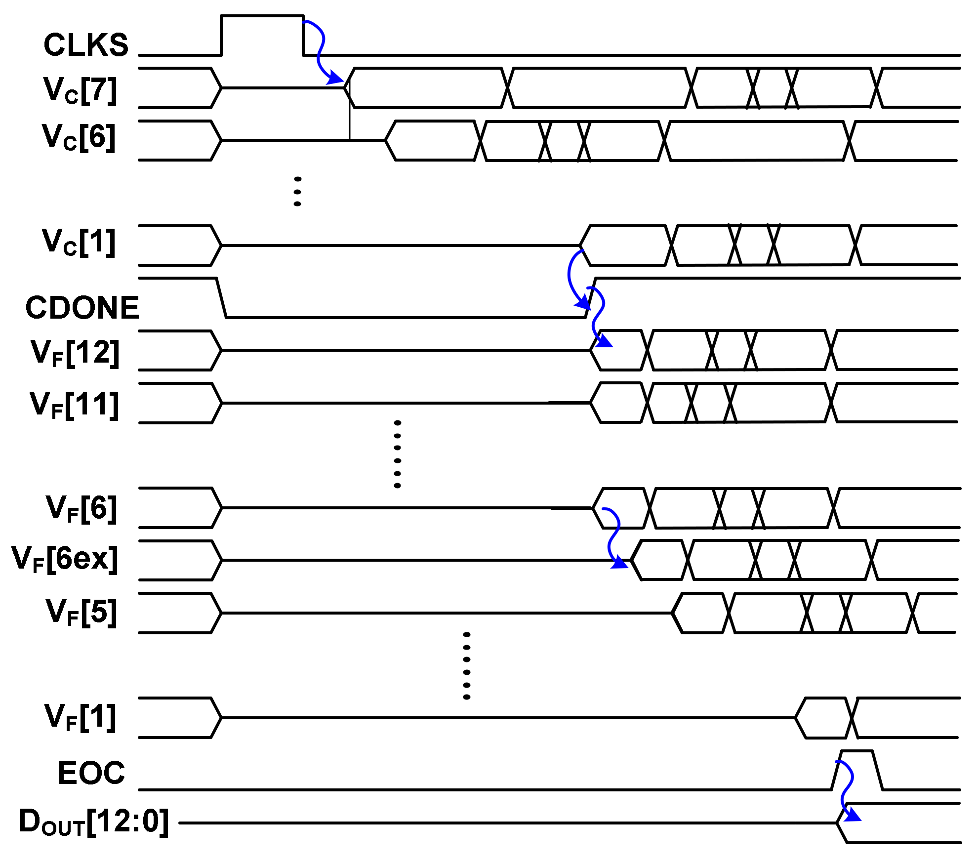
Figure 2 shows the timing sequence of the ADC in conversion mode. It shows the internal DAC control signals, VC[k] (k = 1 to 7) for the coarse ADC, VF[i] (i = 6 to 12) for the MSB segment of the fine ADC, and VF[j] (j = 1 to 5, 6ex) for the LSB segment of the fine ADC. VF[6ex] is the control signal for C6ex, which is an additional capacitor for mismatch calibration. The input signal is sampled into the coarse and fine ADCs by the sampling clock CLKS. All VC[k], VF[i], and VF[j] are connected to VCM. One cycle after CLKS, VC[k] is switched to either VREF or ground, depending on the comparator output. After VC[1] is determined, the signal CDONE becomes high, indicating that the coarse ADC has finished quantization. Then, the DAS controller is enabled, which decodes DOUT,C[12:6] from the coarse ADC to determine VF[i] using the DAS operation. The controller decides which VF[i] is skipped or switched (either VREF or ground) to generate the residue for VDAC,p and VDAC,n of the fine DAC. Here, VDAC,p and VDAC,n are the top-plate voltage of the positive and negative DAC, respectively. The fine ADC waits for one cycle after VF[i] switching so that the values of VDAC,p and VDAC,n are stabilized before it starts quantizing the remaining VF[j].
The input CM voltage is constant during MCS. In the previous work [4,9], the comparator is implemented with a PMOS differential pair because this comparator is designed for monotonic switching. When the previous comparator is used for MCS, it can result in a relatively large offset at the input of the comparator. In this work, we use a comparator having complementary input stages, which allows rail-to-rail range and reduces the kickback noise [14].

2.2. Merged Capacitor Switching with Detect and Skip

Figure 3a shows an example waveform of the DAC when DOUT[9:6] = 0101 is generated using MCS. Figure 3b shows the waveform when MCS and DAS are combined. The two methods generate the same residue for VDAC,p and VDAC,n; however, MCS can waste energy by performing unnecessary switching. By combining MCS and DAS, unnecessary switching can be avoided. The DAS controller decides which capacitor can be skipped for switching. Using DOUT,C[12:6] from the coarse ADC, the DAS operation can be summarized as follows:
(1)
DOUT,C[MSB-1] = DOUT,C[MSB] → switch CMSB|DOUT,C[MSB-1] ≠ DOUT,C[MSB] → skip CMSB,
(2)
DOUT,C[MSB-2] = DOUT,C[MSB] → switch CMSB-1|DOUT,C[MSB-2] ≠ DOUT,C[MSB] → skip CMSB-1, …,
(3)
DOUT,C[MSB-k + 1] = DOUT,C[MSB] → switch CMSB-N+2|DOUT,C[MSB-k + 1] ≠ DOUT,C[MSB] → skip CMSB-N+2,
(4)
Switch CMSB-N+1,
Where MSB = 12 and k is the binary capacitor index of the coarse ADC. We note that the MCS and DAS method is more effective for a relatively smaller input since most switching can be skipped. Because the mismatch effect of the skipped capacitors is also removed, DAS can provide the additional benefit of improved linearity.
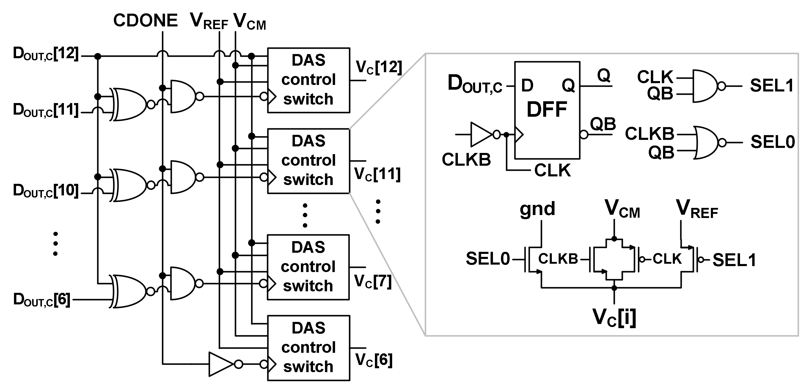
Figure 4 shows the schematic of the DAS controller. When CDONE is enabled, the output DOUT,C[12:6] is input to the DAS control switch through the logic gates. In the beginning, VC[i] is connected to VCM. Depending on the logic value, VC[i] is connected to the ground if DOUT,C[i] is high, or VC[i] is connected to VREF. To evaluate the effectiveness of various switching methods, we compare the switching energy of a 12-bit ADC. The switching energy EMono(i) of the ith capacitor in the monotonic switching can be expressed as
E Mono ( i ) = C N i + 1 C T V REF 2 C T C N i + 1 m = N i + 2 N C m ( b N i + 1 b m ¯ )
where index i is from 1 to N = 12, CT is the total capacitance of each DAC branch, and bm is the binary bit value. The switching energy EMCS(i) of the ith capacitor in the MCS can be expressed as [15]
E MCS ( i ) = 1 2 C N i + 1 2 C T V REF 2 C N i + 1 + 1 2 C N i + 1 C T V REF 2 m = N i + 2 N ( 1 ) b N i + 1 b m ¯ C m
A detailed derivation of Equations (1) and (2) can be found in the Appendix A and Appendix B, respectively. In the subranging ADC, switching energy can be divided into MSB and LSB segments of the DAC. The switching energy of the MSB segment can be expressed as
E DAS ( MSB ) = V REF 2 2 C SW 1 C SW C T
where CSW is the sum of switched capacitors. The switching energy of the LSB segment is calculated using 6-bit MCS. The total switching energy is obtained using
E total = E DAS ( MSB ) + i = 1 6 E MCS ( i )
Figure 5 compares the switching energy of a 12-bit ADC normalized using VREF and the unit capacitor C1. The split capacitor scheme saves 37.5% of energy on average compared with the conventional method [1]. The monotonic switching saves up to 81%. The energy is further reduced using the MCS to 87.5%. Finally, the average switching energy saved is up to 96.7% when combining MCS and DAS in the subranging ADC, which is 9.2% lower than the previous state-of-the-art [7]. This result neglects the energy of the 7-bit coarse ADC, which is relatively small compared to the energy of the 12-bit fine ADC. We note that the switching energy is a normalized value using VREF and C1, independent of the technology node. Relatively low power can still be achieved using the conventional method—for example, 0.084 μW for a 10-bit ADC [8] and 0.38 μW for a 12-bit ADC [16]. Because the SAR ADC is realized using mostly digital logic, except for the comparator, low power can be achieved using scaled-down CMOS technology; the works [8] and [16] are realized using 40 nm and 65 nm CMOS processes, respectively.

3. Mismatch Calibration

3.1. DAC Capacitor Mismatch Calibration

Figure 6a shows one example of a DAC configuration for reading out the mismatch of Ci (i = 6 to 12), one of the 7-bit MSB segments of the DAC. The proposed calibration method reuses the 6-bit DAC to measure the weight error of Ci. The 6-bit DAC consists of 5-bit LSB capacitors (C1 to C5) and one extra capacitor C6ex. Assuming that the 6-bit DAC has sufficient intrinsic linearity, the mismatch of each Ci is sequentially measured. The digital representation DCAL[6:1] of the mismatch is generated from the CAL logic. The positive DAC branch is evaluated first, and the negative DAC branch is calibrated next. During the positive DAC calibration, VDAC,n (negative input of the comparator) is connected to VCM.
Figure 6b shows the waveform of VC[i] during calibration Ci in the positive branch. Here, VC[i] is the control signal connected to the bottom plate of the DAC capacitor. In the sampling phase, VC[i] of all capacitors are connected to VCM. In the next cycle, the bottom plate of the upper group capacitors (C12 to Ci + 1) is connected to VCM, while the bottom plate of the lower group capacitors (Ci−1 to C6) is connected to the ground. The switching results in VDAC,p are
V DAC , p = V CM + ( w i * j = 6 i 1 w j * ) V CM
where w i * is the weight of Ci with mismatch error. Without mismatch, VDAC,p will be equal to VCM. The mismatch causes VDAC,p to deviate from VCM, which is measured by the 6-bit DAC. The bit weight difference between Ci and the sum of lower group capacitors (Ci-1 to C6), which is quantized by the 6-bit DAC, can be expressed as
w i * j = 6 i 1 w j * = j = 1 6 w j b j + q j
where wj is the ideal weight, bj is the binary value, and qj is the quantization error. The values of the LSB segment capacitors (C6ex, C5, …, C1) are assumed to be linear with w j * = w j (j = 1, …, 6).
The C6ex is added to provide sufficient coverage for weight extraction. The value of C6ex is 16CU, which is small compared to the total capacitance CT = 2048CU of each DAC, where CU = C1 is the unit capacitor of the DAC. To simplify the SAR logic, C6ex can be activated only during the calibration mode while connected to VCM in the conversion mode; however, the addition of C6ex causes the actual weight of each capacitor to deviate from the ideal binary weight. The DAC mismatch calibration is based on the idea that the addition of C6ex does not significantly change the weight of each capacitor. To preserve the correct weight of each capacitor, we handle the issue using an alternative approach: (1) C6ex is used in both calibration and conversion mode; in the conversion mode, C6ex serves as a redundant capacitor to improve the ADC linearity; (2) mismatch calibration is designed by including the weight of C6ex; then, the total weight of the 12-bit DAC is increased from 2048 to 2064 (see Table 1).

3.2. Mismatch Error of DAC Capacitor

The VDAC,p and VDAC,n at the inputs of the comparator can be expressed as
V DAC , p = V IN , p + i Ω ( 1 2 b i ) ( w i Δ w pi ) V CM + j = 1 6 ( 1 2 b j ) w j V CM
V DAC , n = V IN , n i Ω ( 1 2 b i ) ( w i Δ w ni ) V CM j = 1 6 ( 1 2 b j ) w j V CM
where VIN,p and VIN,n are the sampled input voltages at the positive and negative DAC, respectively. The bi is the binary value of the DAC capacitor in the MSB segment (C12, …, C6), and bj is the value of capacitors in the LSB segment (C6ex, C5, …, C1). The Ω is the group of switched capacitors by the DAS controller. The wi is the ideal weight of ith capacitor in the MSB segment of the DAC, which is the ratio between Ci and CT. The wj is the ideal weight of the jth capacitor in the LSB segment. The Δwpi and Δwni are the weight errors of the ith capacitor in the positive and negative branches of the fine DAC, respectively. Table 1 shows the ideal weight of each capacitor. The second term of (7) and (8) is the amount of change caused by the mismatch of the MSB capacitors. The third term represents the change caused by the mismatch of the LSB capacitors. At the end of conversion, both VDAC,p and VDAC,n approach VCM as
V IN , p V IN , n + i Ω 1 2 b i 2 w i Δ w pi Δ w ni V CM + 2 j = 1 6 1 2 b j w j V CM 0
Noting VREF = (VIN,p + VIN,n), we can rearrange (9) as
2 V IN , p V REF = i Ω 2 b i 1 w i Δ w pi + Δ w ni 2 + 2 j = 1 6 b j w j + j = 1 6 w j + 1
By multiplying 211 on both sides of (10), we obtain
2 12 V IN , p V REF = 1 2 i Ω 2 b i 1 W i Δ W i + j = 1 6 b j W j + W 0
where Wi = 212wi, ΔWi = (ΔWpi + ΔWni)/2 is the average error of the positive and negative branch, ΔWpi = 212wpi), Wni = 212wni), and W0 = 211(127/129) = 2016.248. At this moment, the weight error ΔWi is unknown, and the method of calculating ΔWi is presented in the next subsection.

3.3. Weight Error Extraction

We assume that the overall mismatch of the DAC is averaged out and normalize the full scale to one [17]. Then, the sum of weight for C12 can be expressed as
w 12 * + i = 6 11 w i * + j = 1 6 w j = 1
The calibration code d12 for C12 can be expressed as
d 12 = w 12 * i = 6 11 w i *
When we substitute (13) into (12), we obtain
1 2 w 12 * = 1 2 j = 1 6 w j d 12
where wj is the weight of the capacitors in the 6-bit DAC. We note that Δ 12 = ( w 12 w 12 * ) Δ12 = (w12w*12) is the weight error of C12 and w12 = (64/129) is the ideal weight of C12. Then, we obtain
Δ 12 = 1 2 j = 1 6 w j d 12 1 258
Similarly, the sum of weight for C11 can be expressed as
w 11 * + i = 6 10 w i * + j = 1 6 w j = 1 w 12 *
Using the calibration code d11 for C11, we obtain
d 11 = w 11 * i = 6 11 w i *
Noting that Δ11 = (w11w*11) Δ 11 = ( w 11 w 11 * ) is the weight error of C11, where w11 = (32/129) is the ideal weight, we obtain
Δ 11 = 1 2 j = 1 6 w j d 11 1 129 Δ 12
Similarly, we obtain the remaining weights. For example, the weight error Δ6 of C6 can be expressed as
Δ 6 = 1 2 j = 1 6 w j d 6 1 129 Δ 12 Δ 11 Δ 10 Δ 9 Δ 8 Δ 7
The digital representation of sampled input VIN,p can be expressed as DIN,p = 212(VIN,p/VREF). Then, the result (10) can be rearranged as
D IN , p = 1 2 i Ω 2 b i 1 W i 1 2 i Ω 2 b i 1 Δ W i + j = 1 6 b j W j + W 0
The first two terms of (20) represent the contribution of the MSB segment of the DAC, which can be positive or negative. The third term is the contribution of the LSB segment. The last term is the average output value. A similar definition can be proposed for DIN,n = 212(VIN,n/VREF) for the sampled input VIN,n. Figure 7 shows the block diagram implementing Equation (20) to calculate DIN,p. Using the logic value of the skipped MSB group, it calculates the contribution of the MSB and LSB segment capacitors. The calculation is performed off-chip using Matlab.
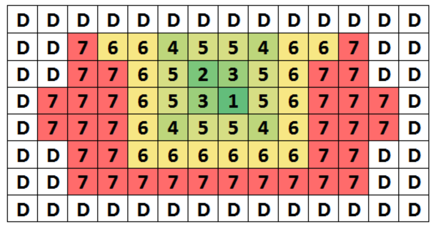
Figure 8 shows the floor plan of the coarse DAC. We use a common-centroid layout to reduce the capacitor mismatch. Because capacitors need to be connected to the outside of the DAC, the metal route increases the coupling with neighboring capacitors. The effect of additional coupling is usually more sensitive to small capacitors. We reduce the effect by placing the capacitors of the LSB segment close to the edge of the DAC. Dummy capacitors are added around the DAC periphery to reduce the mismatch caused by the edge effect. A similar technique is used for the fine DAC.
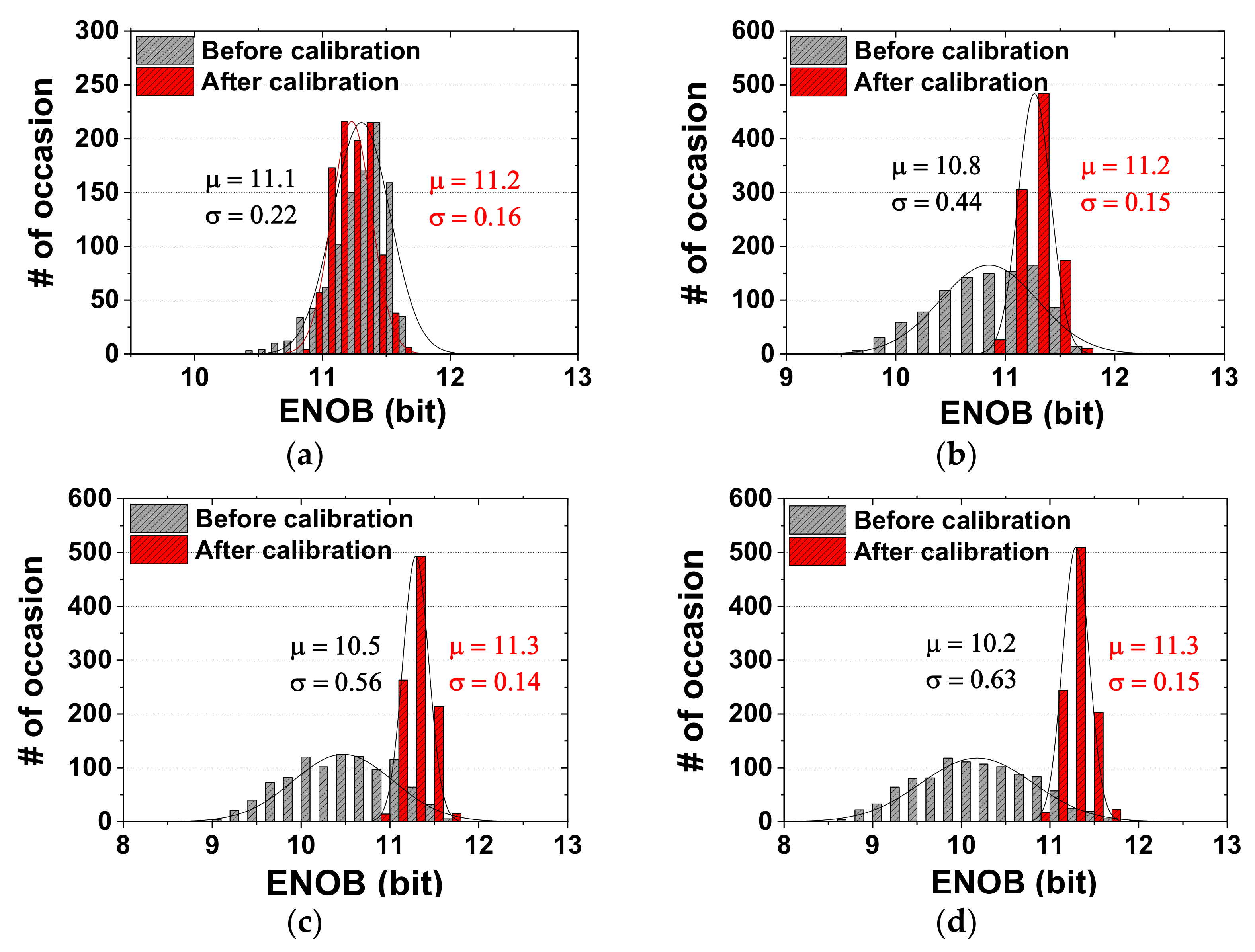
We use a behavioral model to investigate the ADC performance depending on the mismatch. Monte Carlo simulations with 1000 samples are performed using the DAC capacitor mismatch rate of 1.0%, 1.5%, 2.0%, and 2.5%. Figure 9 compares the effective number of bits (ENOB) probability distribution before and after calibration. Before calibration, the average ENOB decreases from 11.1 bits to 10.2 bits when the mismatch increases from 0.5% to 2%. In the case of a 1% mismatch, the average ENOB increases from 10.8 bits to 11.2 bits after calibration. The standard deviation is reduced from 0.44 bit to 0.15 bit. In the case of a 1.5% mismatch, the average ENOB improves from 10.5 bits to 11.3 bits. The result shows that calibration effectively handles ENOB degradation with the mismatch rate. The minimum capacitor value allowed by the process is 21.2 fF (4 × 4 μm2). Based on the process datasheet, the unit capacitor in the coarse DAC is designed to be larger than the minimum value to achieve a 1% mismatch rate, which is 54 fF (6.72 × 6.72 μm2). Figure 10 shows the power breakdown of the ADC. Overall power including output buffer is 5.08 μW at fS = 200 kS/s. The breakdown shows that the SAR logic of fine ADC, the DAS controller, and the SAR logic of coarse ADC consume 39.5%, 18.9%, and 16.7% of the overall power, respectively.

4. Measured Results

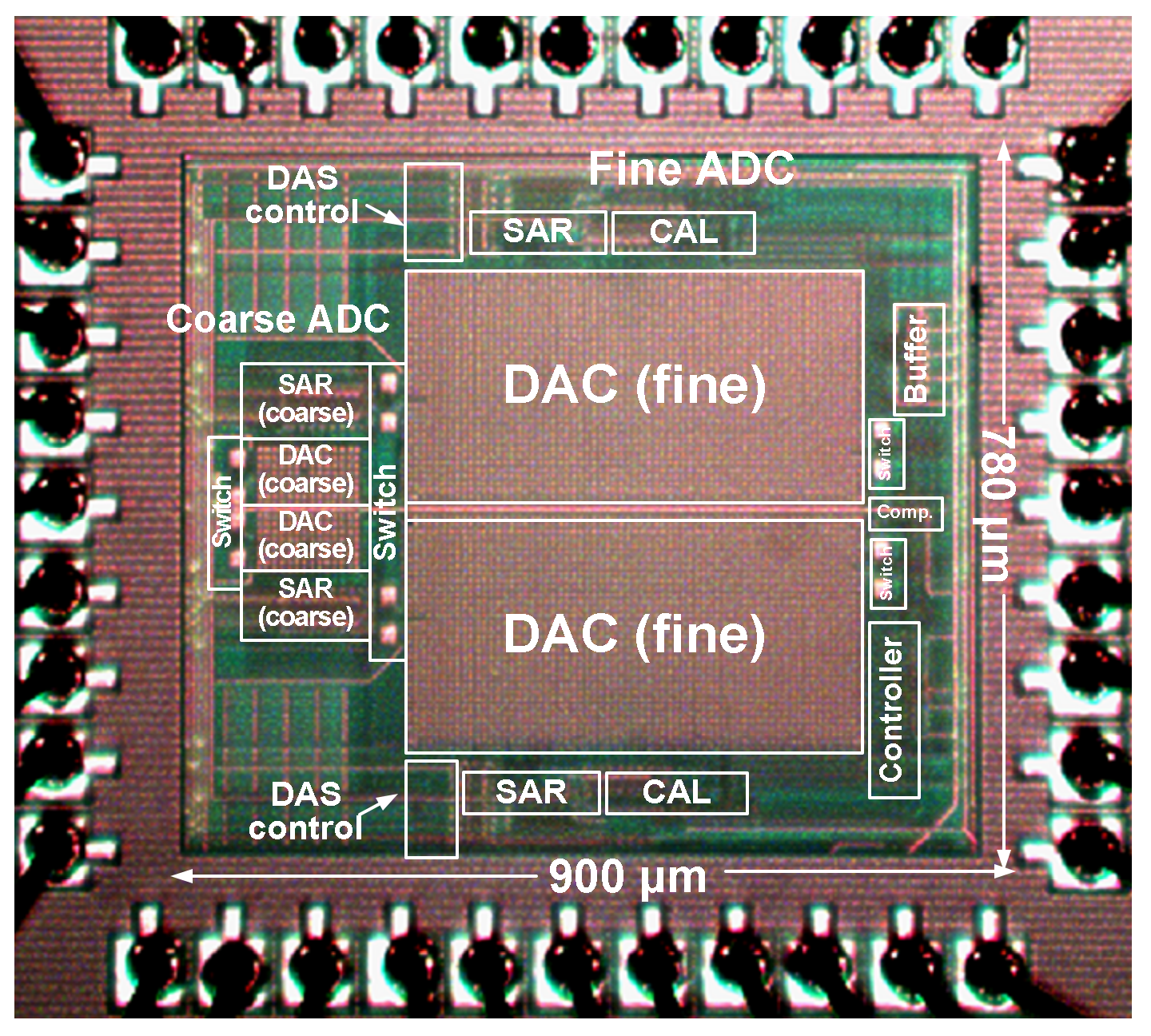
Figure 11 shows a microphotograph of the ADC fabricated in a 0.18 μm CMOS process. The core area is 0.7 mm2. The coarse ADC occupies 8.5% of the overall area. The IC is mounted on a test board using the chip-on-board (COB) technique. Biopotentials typically exhibit signal frequencies less than 1 kHz. In this measurement, we choose an input frequency fIN = 1.12k kHz.
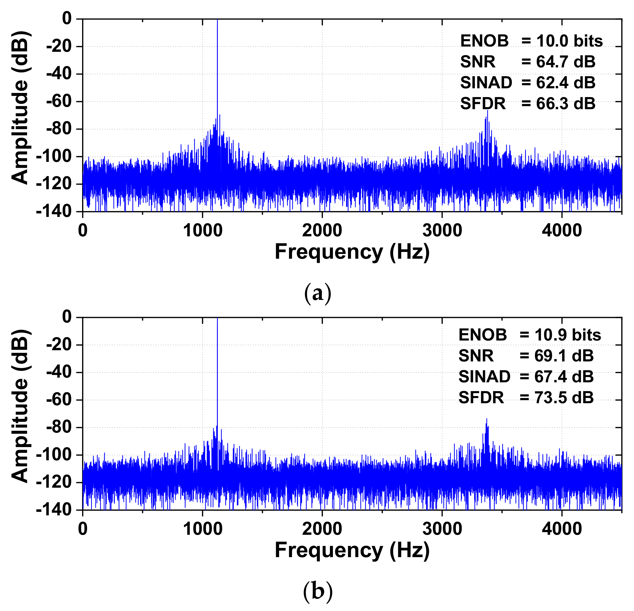
Figure 12 shows the comparison of the measured output spectra of the ADC before and after calibration. A differential sinusoidal signal with 0.9 V amplitude is applied for dynamic performance testing. The measured data are obtained from the fast Fourier transform (FFT) spectrum with 32768 points. After calibration, SINAD and SFDR are improved by 5.04 dB and 7.21 dB, respectively, resulting in an ENOB of 10.9 bits. The third harmonic located at 3fIN, which is related to the nonlinearity of the ADC, is reduced from −66.3 dB to −77.2 dB. Figure 13 shows the output spectrum using a near-Nyquist input frequency and the sampling rate fS = 9 kS/s. The SINAD and SFDR are improved by 5.44 dB and 2.94 dB, respectively, resulting in an ENOB of 10.5 bits.
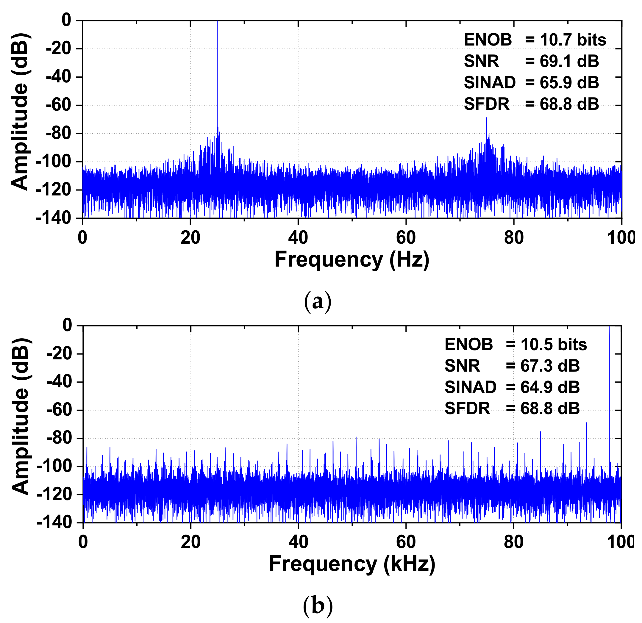
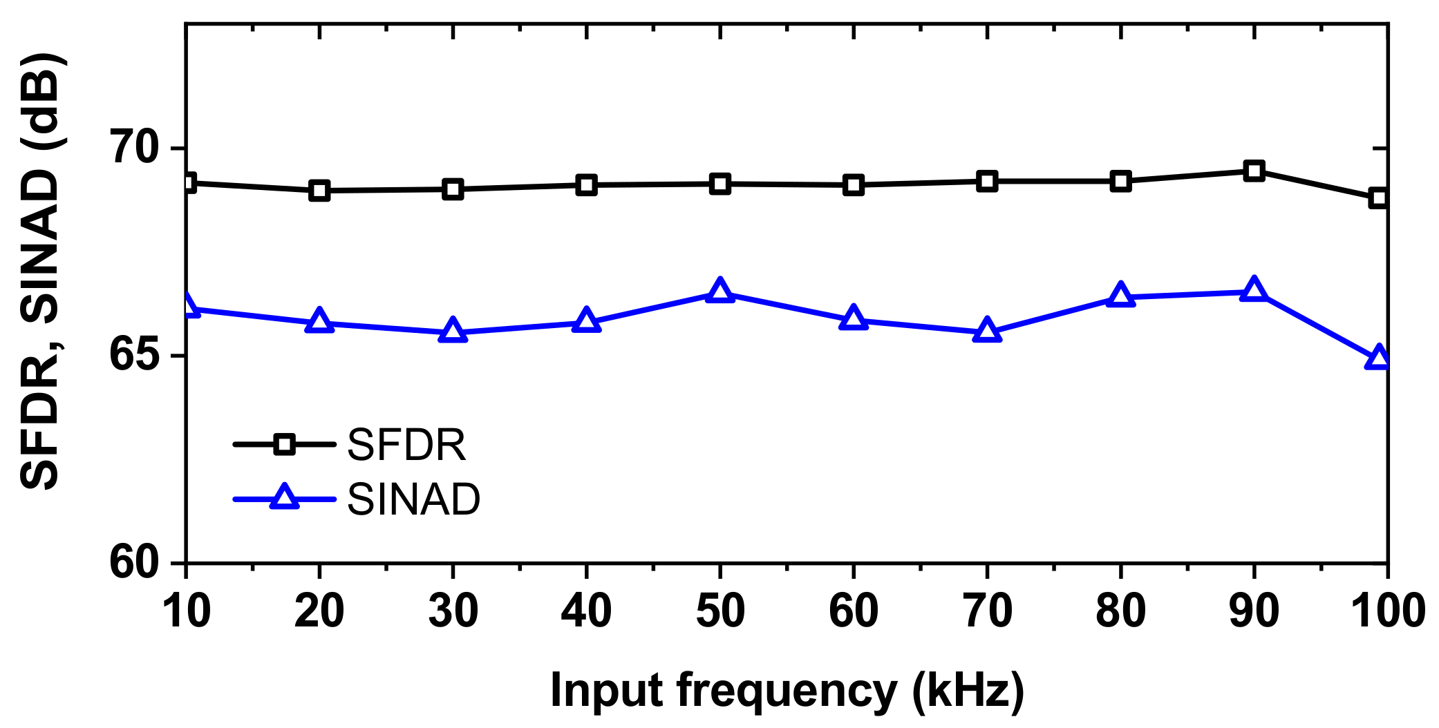
Additionally, we characterize the dynamic performance at increased fIN. Figure 14 shows the measured spectra of the ADC at fIN = 24.981 kHz and 97.857 kHz (near the Nyquist frequency) after the calibration. The ADC achieves a SINAD of 65.9 dB and an SFDR of 68.8 dB for fIN = 24.981 kHz. The level of the third harmonic located at 3fIN is −68.7 dB, indicating that further improvement of the ADC nonlinearity is needed. Figure 15 shows the measured SFDR and SINAD as a function of fIN. The effective resolution bandwidth (ERBW) is the input frequency where the SINAD drops by 3 dB (1/2 LSB or 0.5 bit) from its value for low-frequency input. The result shows that ERBW is around 100 kHz, approximately half of the sampling frequency (Nyquist frequency).
Figure 16 compares the differential nonlinearity (DNL) and integral nonlinearity (INL) of the ADC before and after calibration. A total of 32786 codes are collected to build a histogram. Both INL and DNL are improved, and the calibration has a more desirable effect on INL than DNL, as expected. The peak INL decreases from +3.4/−3.48 LSB to +2.05/−2.24 LSB. The peak DNL is +2.19/−1 LSB before calibration, improving to +1.31/−1 LSB.
Table 2 shows the comparison with the previous works. The work in [8] presents a subranging SAR ADC using the DAS method. They use split capacitor switching, which consumes more energy than MCS. A similar observation can be made for the work in [16], which uses the swap-to-reset DAC switching method. The low power consumption can be attributed to the scaled-down technology, 65 nm CMOS [16] and 40 nm CMOS [8,18]. When we compare the ADC realized using a similar CMOS process [2,19], our work achieves a better Walden’s figure-of-merit (FOMW) of 13.2 fJ/conv.-step and Schreier’s figure-of-merit (FOMS) of 170.4 dB. The work in [11] presents a 13-bit SAR ADC with on-chip calibration realized in a relatively large area (0.9 mm2) using a 0.13 μm CMOS process. Our work realizes the subranging ADC, consisting of coarse and fine ADC, in 0.7 mm2 using a 0.18 μm CMOS process. The work in [20] presents good dynamic performance; however, it consumes relatively high power, leading to an FoMS of 114.5 dB.
The footnote shows the relationship between ENOB and SINAD. This equation does not explicitly consider the process gain related to the FFT. We can estimate the process gain using GFFT = 10∙log(NF/2), where NF is the number of points processed in the FFT. Each nth FFT bin can be considered as the output from a narrow bandpass filter with a center frequency at (nfS/NF). A large number of samples improves the frequency resolution and decreases the amount of noise in the bin’s passband. For an NF-point FFT, the average value of the noise contained in each frequency bin is reduced by GFFT below the root-mean-square (rms) value of the quantization noise.

5. Conclusions

We investigate a 12-bit subranging SAR ADC for low-power biopotential sensing applications. A new DAC switching method is proposed by combining the MCS and DAS methods, successfully embedded in the subranging structure. Analysis of the DAC switching energy shows that the proposed method saves 96.7% of switching energy compared to the conventional method. To handle the DAC mismatch, we implement digital domain calibration without the extra burden of an on-chip calibration circuit. A simple method of extracting the weight error is presented by reusing the 6-bit DAC. The mismatch data are successfully processed in the digital domain to compensate for the nonlinearity caused by the DAC mismatch. The proposed ADC fabricated in 0.18 μm CMOS demonstrates successful operation and performance improvement using the proposed calibration technique. At a sampling rate of 200 kS/s, the ADC achieves SINAD of 65.9 dB and SFDR of 68.8 dB, with an FoM of 13.2 fJ/conversion- step. The contributions of this paper can be summarized as follows: (1) this work proposes an energy-efficient DAC switching method by combining MCS and DAS, (2) the proposed switching method is successfully implemented in a 12-bit subranging ADC, and (3) this work proposes a digital domain calibration using a normalized full-scale weight method. The result will be useful for realizing a low-power ADC for battery-powered, portable biomedical sensing applications.

Author Contributions

C.L.N. designed the ADC and setup, performed the experimental work, and wrote the manuscript. H.N.P. designed the mismatch calibration algorithm and wrote the manuscript. J.-W.L. conceived the project, organized the paper’s content, and edited the manuscript. Corresponding author: J.-W.L. All authors have read and agreed to the published version of the manuscript.

Funding

This work was supported in part by the Basic Science Research Program through the National Research Foundation of Korea (No. 2021R1A2B5B01001475) and in part by National R&D Program through the National Research Foundation of Korea funded by the Ministry of Science and ICT (No. 2020M3H2A1076786).

Acknowledgments

The chip fabrication and CAD tools were supported by the IDEC (IC Design Education Center).

Conflicts of Interest

The authors declare no conflict of interest.

Appendix A. Monotonic Switching

Figure A1 shows the monotonic switching diagram for a 3-bit example (N = 3). After the sampling switches are turned off, the comparator directly performs the first comparison without switching any capacitor.
Figure A1. Monotonic switching diagram for a 3-bit ADC.
Sensors 22 03600 g0a1
(1) After the first comparison, the MSB bit bN is determined. The bottom plate of capacitor CN (positive DAC branch if bN = 1 or negative DAC branch if bN = 0) is switched to the ground. Then, the comparator input (VDAC,p if bN = 1 or VDAC,n if bN = 0) is reduced by an amount of (CN/CT)VREF. The total capacitance connected to VREF is (CTCN) in the corresponding DAC branch. The switching energy that VREF supplies to the DAC at the first cycle (ϕ1) can be expressed as
E Mono ( 1 ) = C N C T V REF 2 C T C N = 1 2 V REF 2 C N = C V REF 2
where CN = 2C, CT = 4C is the total capacitance of each DAC branch, and C is the unit capacitance.
(2) After the second comparison, bN−1 is determined. The bottom plate of capacitor CN−1 (positive DAC branch if bN−1 = 1 or negative DAC branch if bN−1 = 0) is switched to the ground. Then, the comparator input is reduced by (CN−1/CT)VREF. We consider the four cases as follows:
-
If bN = 0, bN−1 = 0: total capacitance connected to VREF of the negative DAC branch is CTCN−1CN;
-
If bN = 0, bN−1 = 1: total capacitance connected to VREF of the positive DAC branch is CTCN−1;
-
If bN = 1, bN−1 = 0: total capacitance connected to VREF of the negative DAC branch is CTCN−1;
-
If bN = 1, bN−1 = 1: total capacitance connected to VREF of the positive DAC branch is CTCN−1CN.
We can express the four cases using a single equation that describes the total capacitance connected to VREF as
C T C N 1 ( b N 1 b N ¯ ) C N
where (bN−1 bN) is the XOR of the current bit (bN) and the previous bit (bN−1) value.
The switching energy that VREF supplies to the DAC at the second cycle (ϕ2) can be expressed as
E Mono ( 2 ) = C N 1 C T V REF 2 C T C N 1 ( b N 1 b N ¯ ) C N
(3) After the third comparison, bN−2 is determined. The bottom plate of capacitor CN−2 is switched to the ground. The comparator input is reduced by an amount of (CN−2/CT)VREF. There are eight switching cases, and we can express the cases using a single equation that describes the total capacitance connected to VREF as
C T C N 2 ( b N 2 b N ¯ ) C N ( b N 2 b N 1 ¯ ) C N 1
The switching energy that VREF supplies to the DAC at the third cycle (ϕ3) can be expressed as
E Mono ( 3 ) = C N 2 C T V REF 2 C T C N 3 + 1 ( b N 2 b N ¯ ) C N ( b N 2 b N 1 ¯ ) C N 1   = C N 3 + 1 C T V REF 2 C T C N 3 + 1 m = N 3 + 2 N C m ( b N 3 + 1 b m ¯ )
By generalizing the above result for an N-bit ADC, we obtain Equation (1) of the main text.

Appendix B. Merged Capacitor Switching

Figure A2 shows the merged capacitor switching diagram for a 3-bit example. After the sampling switches are turned off, the comparator directly performs the first comparison without switching any capacitor. Switching energy calculation is similar to monotonic switching, except that switching is performed from VCM rather than VREF.
(1) After the first comparison, the MSB bit bN is determined. The bottom plate of capacitor CN (positive DAC branch if bN = 1 or negative DAC branch if bN = 0) is switched from VCM to VREF. Then, one comparator input (VDAC,p if bN = 1 or VDAC,n if bN = 0) is increased by the amount of (CN/CT)(VREF/2). The opposite comparator input is reduced by the amount of (CN/CT)(VREF/2). The total capacitance connected to VREF is CN. The switching energy that VREF supplies to the DAC at the first cycle (ϕ1) can be expressed as
E MCS ( 1 ) = 1 2 C N 2 C T V REF 2 C N = 1 2 1 4 V REF 2 2 C = C V REF 2 2
(2) After the second comparison, bN−1 is determined. The bottom plate of capacitor CN−1 (positive DAC branch if bN−1 = 1 or negative DAC branch if bN−1 = 0) is switched from VCM to VREF. Then, one comparator input is increased by the amount of (CN−1/CT)(VREF/2). The opposite comparator input is reduced by the amount of (CN−1/CT)(VREF/2). We consider one of the four cases (bN = 0, bN−1 = 0). There are two capacitors (CN and CN−1) in the positive branch connected to VREF. The energy that VREF supplies to the DAC at this step can be expressed as
E MCS ( 2 ) = V REF V CM C N 1 C T V REF 2 C N 1 V REF + V REF V REF C N 1 C T V REF 2 C N V REF   = 1 2 C N 1 2 C T C N 1 V REF 2 1 2 C N 1 C T V REF 2 C N = 1 8 C V REF 2
Similar equations can be derived for the remaining three cases. Then, we can express the four cases using a single equation, and the switching energy at ϕ2 can be expressed as
E MCS ( 2 ) = 1 2 C N 1 2 C T V REF 2 C N 1 ± 1 2 C N 1 C T V REF 2 C N   = 1 2 C N 1 2 C T V REF 2 C N 1 + 1 2 C N 1 C T V REF 2 ( 1 ) b N 1 b N ¯ C N = 3 8 V REF 2 C ± 2 8 V REF 2 C
where the ± sign is replaced with ( 1 ) b N 1 b N ¯ .
Figure A2. Merged capacitor switching diagram for a 3-bit ADC.
Sensors 22 03600 g0a2
(3) After the third comparison, bN−2 is determined. There are eight cases, and we can express the cases using a single equation. Then, the switching energy at ϕ3 can be expressed as
E MCS ( 3 ) = 1 2 C N 2 2 C T V REF 2 C N 2 + 1 2 C N 2 C T V REF 2 ± C N ± C N 1   = 1 2 C N 2 2 C T V REF 2 C N 2 + 1 2 C N 2 C T V REF 2 ( 1 ) b N 2 b N ¯ C N + ( 1 ) b N 2 b N 1 ¯ C N 1
where the first ± sign in the second term is replaced with ( 1 ) b N 2 b N ¯ , and the second ± sign is replaced with ( 1 ) b N 2 b N 1 ¯ . By generalizing the above result, we obtain Equation (2) of the main text.

References

  1. Saberi, M.; Lotfi, R.; Mafinezhad, K.; Serdijn, W.A. Analysis of power consumption and linearity in capacitive digital-to-analog converters used in successive approximation ADCs. IEEE Trans. Circuits Syst. I Reg. Pap. 2011, 58, 1736–1748. [Google Scholar] [CrossRef]
  2. Sadollahi, M.; Temes, G. An 11-bit 250-nW 10-kS/s SAR ADC with doubled input range for biomedical application. In Proceedings of the IEEE International Midwest Symposium on Circuits and Systems, Boston, MA, USA, 6–9 August 2017; pp. 385–388. [Google Scholar]
  3. Yoshioka, M.; Ishikawa, K.; Takayama, T.; Tsukamoto, S. A 10-b 50-MS/s 820-μW SAR ADC with on-chip digital calibration. IEEE Trans. Biomed. Circuits Syst. 2010, 4, 410–416. [Google Scholar] [CrossRef] [PubMed]
  4. Liu, C.; Chang, S.; Huang, G.; Lin, Y. A 10-bit 50-MS/s SAR ADC with a monotonic capacitor switching procedure. IEEE J. Solid-State Circuits 2010, 45, 731–740. [Google Scholar] [CrossRef]
  5. Liu, C.; Chang, S.; Huang, G.; Lin, Y. A 0.92 mW 10-bit 50-MS/s SAR ADC in 0.13 μm CMOS process. In Proceedings of the Symposium on VLSI Circuits, Digest of Technical Papers, Kyoto, Japan, 16–18 June 2009; pp. 236–237. [Google Scholar]
  6. Chang, Y.; Wang, C.; Wang, C. A 8-bit 500-KS/s low power SAR ADC for biomedical applications. In Proceedings of the IEEE Asian Solid-State Circuits Conference, Jeju, Korea, 12–14 November 2007; pp. 228–231. [Google Scholar]
  7. Hariprasath, V.; Guerber, J.; Lee, S.-H.; Moon, U. Merged capacitor switching based SAR ADC with highest switching energy-efficiency. Electron. Lett. 2010, 46, 620–621. [Google Scholar] [CrossRef] [Green Version]
  8. Tai, H.-Y.; Hu, Y.-S.; Chen, H.-W.; Chen, H.-S. A 0.85fJ/conversion-step 10b 200 kS/s subranging SAR ADC in 40nm CMOS. In Proceedings of the IEEE International Solid-State Circuits Conference Digest of Technical Papers, San Francisco, CA, USA, 9–13 February 2014; pp. 196–197. [Google Scholar]
  9. Lee, J.H.; Park, D.; Cho, W.; Phan, H.N.; Nguyen, C.L.; Lee, J.-W. A 1.15 μW, 200 kS/s 10-b monotonic SAR ADC using dual on-chip calibrations and accuracy enhancement techniques. Sensors 2018, 18, 3486. [Google Scholar] [CrossRef] [PubMed] [Green Version]
  10. Um, J.Y.; Kim, Y.-J.; Song, E.-W.; Sim, J.-Y.; Park, H.-J. A digital-domain calibration of split-capacitor DAC for a differential SAR ADC without additional analog circuits. IEEE Trans. Circuits Syst. I Reg. Pap. 2013, 60, 2845–2856. [Google Scholar] [CrossRef]
  11. Ha, H.S.; Lee, S.-K.; Kim, B.S.; Park, H.-J.; Sim, J.-Y. A 0.5-V, 1.47-μW 40-kS/s 13-bit SAR ADC with capacitor error compensation. IEEE Trans. Circuits Syst. II Exp. Briefs 2014, 61, 840–844. [Google Scholar] [CrossRef]
  12. Liu, W.; Huang, P.; Chiu, Y. A 12-bit 45-MS/s, 3-mW redundant successive-approximation-register analog-to-digital converter with digital calibration. IEEE J. Solid-State Circuits 2011, 46, 2661–2672. [Google Scholar] [CrossRef]
  13. Zhang, D.; Alvandpour, A. Analysis and calibration of nonbinary-weighted capacitive DAC for high-resolution SAR ADCs. IEEE Trans. Circuits Syst. II Exp. Briefs 2014, 61, 666–670. [Google Scholar] [CrossRef] [Green Version]
  14. Choi, C.; Lee, J.-W. An 11.8-fJ/conversion-step noise shaping SAR ADC with embedded passive gain for energy-efficient IoT sensors. Sensors 2022, 22, 869. [Google Scholar] [CrossRef] [PubMed]
  15. Guerber, J.; Venkatram, H.; Oh, T.; Moon, U. Enhanced SAR ADC energy efficiency from the early reset merged capacitor switching algorithm. In Proceedings of the IEEE International Symposium on Circuits and Systems, Seoul, Korea, 20–23 May 2012; pp. 2361–2364. [Google Scholar]
  16. Liu, M.; Roermund, A.; Harpe, P. A 7.1fJ/conv.-step 88 dB-SFDR 12b SAR ADC with energy-efficient swap-to-reset. In Proceedings of the IEEE European Solid-State Circuits Conference, Lausanne, Switzerland, 12–15 September 2016; pp. 409–412. [Google Scholar]
  17. Chang, D.-J.; Kim, W.; Seo, M.-J.; Hong, H.-K.; Ryu, S.-T. Normalized-full-scale-referencing digital-domain linearity calibration for SAR ADC. IEEE Trans. Circuits Syst. I Reg. Pap. 2017, 64, 322–332. [Google Scholar] [CrossRef]
  18. Lim, Y.; Flynn, M.P. A 1 mW 71.5 dB SNDR 50 MS/s 13 bit fully differential ring amplifier based SAR-assisted pipeline ADC. IEEE J. Solid-State Circuits 2015, 50, 2901–2911. [Google Scholar] [CrossRef]
  19. Ding, M.; Harpe, P.; Liu, Y.-H.; Busze, B.; Philips, K.; Groot, H. A 46 μW 13 b 6.4 MS/s SAR ADC with background mismatch and offset calibration. IEEE J. Solid-State Circuits 2016, 52, 423–432. [Google Scholar] [CrossRef] [Green Version]
  20. Chen, L.; Sanyal, A.; Ma, J.; Sun, N. A 24-μW 11-bit 1-MS/s SAR ADC with a bidirectional single-side switching technique. In Proceedings of the IEEE European Solid State Circuits Conference, Venice, Italy, 22–26 September 2014; pp. 219–222. [Google Scholar]
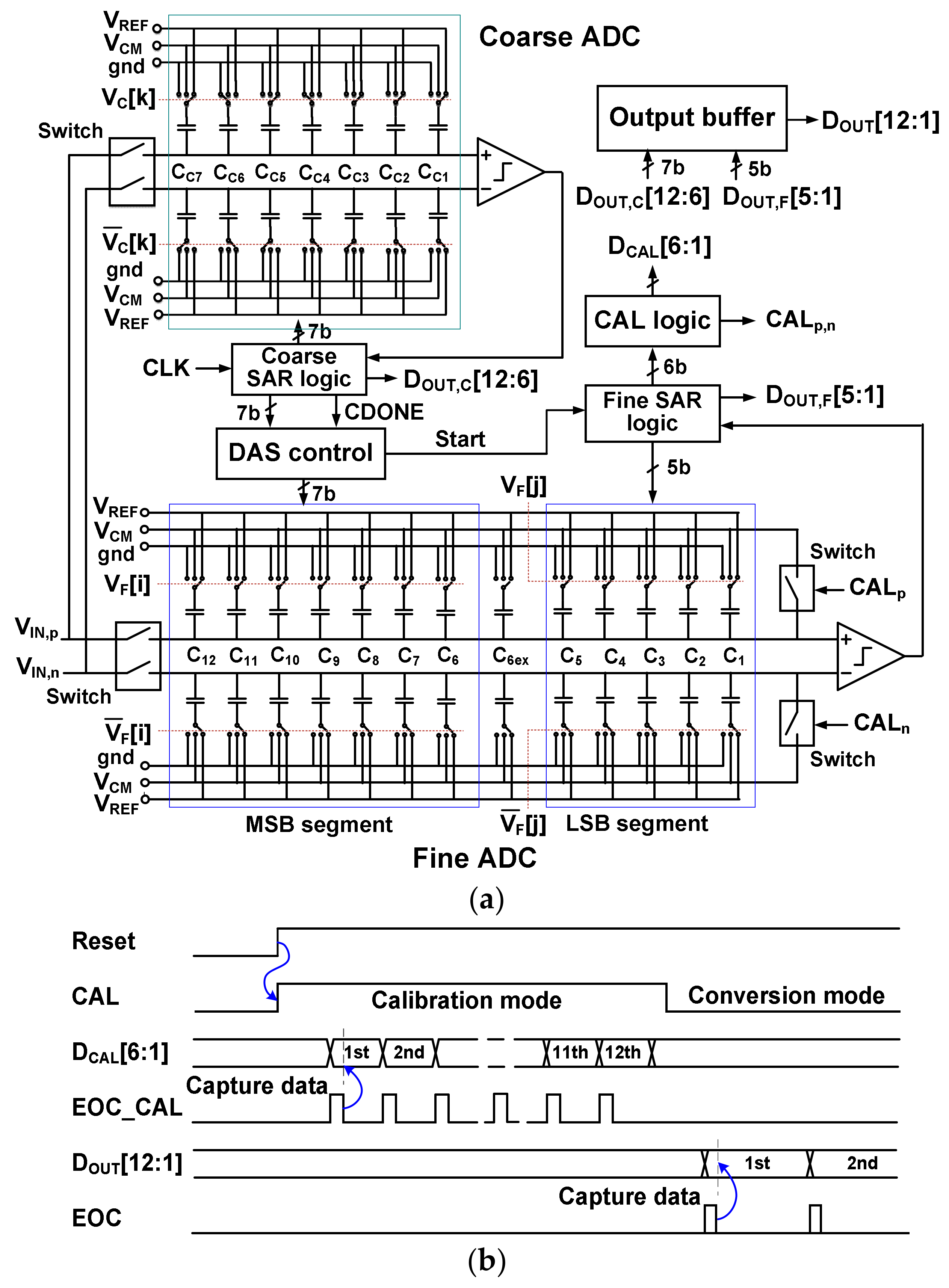
Figure 1. (a) Block diagram of the subranging ADC. (b) Timing sequence of the ADC.
Sensors 22 03600 g001
Figure 2. Timing sequence of the ADC in the conversion mode.
Sensors 22 03600 g002
Figure 3. Example waveform of the DAC switching using (a) MCS only, (b) MCS and DAS method.
Sensors 22 03600 g003
Figure 4. Schematic of the DAS controller.
Sensors 22 03600 g004
Figure 5. Comparison of the DAC switching energy.
Sensors 22 03600 g005
Figure 6. (a) Example DAC configuration for reading out the mismatch of the capacitor Ci. (b) Waveforms of the control signal VC[i] at the bottom plate of the DAC capacitor during calibration Ci.
Sensors 22 03600 g006
Figure 7. Block diagram of processing of the calibrated digital output.
Sensors 22 03600 g007
Figure 8. Floor plan of the coarse DAC.
Sensors 22 03600 g008
Figure 9. Comparison of the ENOB probability distribution before and after calibration. Mismatch rate is (a) 0.5%, (b) 1.0%, (c) 1.5%, (d) 2.0%.
Sensors 22 03600 g009
Figure 10. Power breakdown of the ADC.
Sensors 22 03600 g010
Figure 11. Microphotograph of the fabricated ADC.
Sensors 22 03600 g011
Figure 12. Measured output spectra of the ADC (a) before calibration, (b) after calibration. fIN = 1.124 kHz, fS = 9 kS/s.
Sensors 22 03600 g012
Figure 13. Measured output spectra of the ADC (a) before calibration, (b) after calibration. fIN = 4.403 kHz, fS = 9 kS/s.
Sensors 22 03600 g013
Figure 14. (a) Measured output of the ADC. (b) Measured output near the Nyquist frequency. fS = 200 kS/s.
Sensors 22 03600 g014
Figure 15. Measured SINAD and SFDR at different input frequencies. fS = 200 kS/s.
Sensors 22 03600 g015
Figure 16. Measured static nonlinearity of the ADC.
Sensors 22 03600 g016
Table 1. Ideal weight of DAC.
DAC CapacitorCapacitance (CU)Ideal Weight
C12102464/129
C1151232/129
C1025616/129
C91288/129
C8644/129
C7322/129
C6161/129
C6ex161/129
C581/258
C441/516
C321/1032
C211/2064
C111/2064
Total20641
Table 2. Performance comparison.
[2][8][11][16][18][19][20]This Work
Tech. (nm)18040130654018065180
Supply (V)0.750.450.50.81.01.01.21.8/1.0
Resolution (bit)1110131213111312
Rate (kS/s)1020040406400100050,000200
SINAD (dB)60.555.666.364.264.163.470.967.4
SFDR (dB)72.076.271.088.268.876.684.673.5
ENOB (bit)9.88.9510.710.410.410.311.510.9
CalibrationNoNoYesNoYesNoNoYes
Power (μW)0.250.0841.470.38462410005.08
Area (mm2)0.130.0070.90.110.070.10.050.7
FoMW *
(fJ/conv.-step)
28.80.8521.87.12.219.96.913.2
FoMS ** (dB)163.5176.4167.6171.5172.5166.6114.9170.4
ENOB = (SINAD − 1.76)/6.02. *   FoM W = Power f S × 2 ENOB , * *   FoM S = SIN AD + 10 log f S 2 × Power .
Publisher’s Note: MDPI stays neutral with regard to jurisdictional claims in published maps and institutional affiliations.