Abstract
This article reports on a compact and low-power CMOS readout circuit for bioelectrical signals based on a second-order delta-sigma modulator. The converter uses a voltage-controlled, oscillator-based quantizer, achieving second-order noise shaping with a single opamp-less integrator and minimal analog circuitry. A prototype has been implemented using 0.18 μm CMOS technology and includes two different variants of the same modulator topology. The main modulator has been optimized for low-noise, neural-action-potential detection in the 300 Hz–6 kHz band, with an input-referred noise of 5.0 μVrms, and occupies an area of 0.0045 mm2. An alternative configuration features a larger input stage to reduce low-frequency noise, achieving 8.7 μVrms in the 1 Hz–10 kHz band, and occupies an area of 0.006 mm2. The modulator is powered at 1.8 V with an estimated power consumption of 3.5 μW.
1. Introduction
Electrogenic cells, such as neurons, cardiac cells, or retinal cells, generate ionic currents across their membrane owing to the different ion channels that populate the cellular membranes. Transmembrane ionic currents produce voltage variations in the extracellular medium that can be detected by miniaturized sensors in close proximity to the cells. These voltage signals occur in different frequency bands and feature different amplitudes depending on their nature: neural action potentials (APs) manifest as spikes with amplitudes ranging from a few tens of μV to 1 mV and most signal power between 300 Hz and 6 kHz, whereas cardiac field potentials may reach tens of mV with most signal power in the 1 Hz–1 kHz band. The development of sensors, capable of simultaneously detecting action potentials of multiple cells, enables advanced electrophysiology studies, improving the understanding of complex signaling and opening paths to restoring lost functions. CMOS technology allows for low-noise recording from thousands of electrodes in parallel, either in vitro [1] or in vivo [2]. In vitro studies can be performed with CMOS microelectrode arrays (MEAs), the electrode array of which is co-integrated with the readout electronics [3]. In vivo interfaces commonly make use of passive probes connected to external readout arrays [2,4,5], although a variety of monolithic silicon probes combining electrodes and electronics on the same die have been developed [6,7].
In order to detect APs with acceptable signal-to-noise ratios, recording front-ends require input-referred noise values below 10 μVrms. This is especially relevant for neural interfaces, where small action potentials generated by different neurons need to be separated and assigned to the respective signal sources. CMOS technology allows for simultaneously recording from thousands of densely packed electrodes at a high spatiotemporal resolution, and it allows for conditioning and digitizing signals on-chip with low noise. Advanced signal post-processing (e.g., spike-sorting [8]) is frequently performed off-chip, due to the limited computing power of on-chip processors. This relieves the specifications of on-chip readout circuits, since some effects of circuit impairments, such as signal distortion, power-supply noise, and process variations, can be mitigated by means of calibration and post-processing. Furthermore, current trends in CMOS neural interfaces point towards low-power readout circuits, which enable the integration of tens of thousands of readout channels into the overall system without excessive power consumption and heat dissipation. A small footprint per channel is desired to minimize the area of the overall neural interface, which can easily exceed 100 mm2 [3,9].
Current state-of-the-art implementations of neural interfaces include a wide variety of analog-to-digital converter (ADC) topologies, such as successive approximation registers (SAR) [3,10,11,12], analog-to-time converters (ATC) [13], single-slope (SS) architectures [9,14], and different combinations of delta (∆) and delta-sigma (∆Σ) modulators [5,15,16,17]. ∆Σ modulators are well suited to low-frequency applications owing to noise-shaping, which reduces in-band quantization noise by means of high-pass filtering [18]. The in-band quantization noise depends on the sampling frequency and on different design parameters pertaining to the complexity of the modulator, such as the order of the high-pass filter and the number of bits of the quantizer. Voltage-control-oscillator (VCO)-quantizers have emerged as efficient implementations that provide one additional order of noise-shaping to the modulator [19,20]. This article presents a readout circuit for bioelectrical signals based on a continuous-time second-order ∆Σ modulator. Second-order noise-shaping is achieved by combining a single-loop first-order modulator with a 1-bit VCO-based quantizer. Analog circuitry has been simplified to reduce area and power consumption, while the circuit relies on off-chip digital post-processing for filtering, down-sampling, and further corrections. The prototype includes two variants of the same design: one design has been optimized for small real estate and action potential detection in the 300 Hz–6 kHz band, while the second design features a larger input stage to minimize the noise in the 1 Hz–10 kHz band.
This paper is organized as follows: In Section 2, the block diagrams of the proposed modulator and the circuits of the key building blocks are shown and described. The electrical characterization of the prototype is shown in Section 3, and the results of in vitro testing with cardiomyocytes are reported in Section 4. Finally, Section 5 concludes the paper.
2. Readout Design
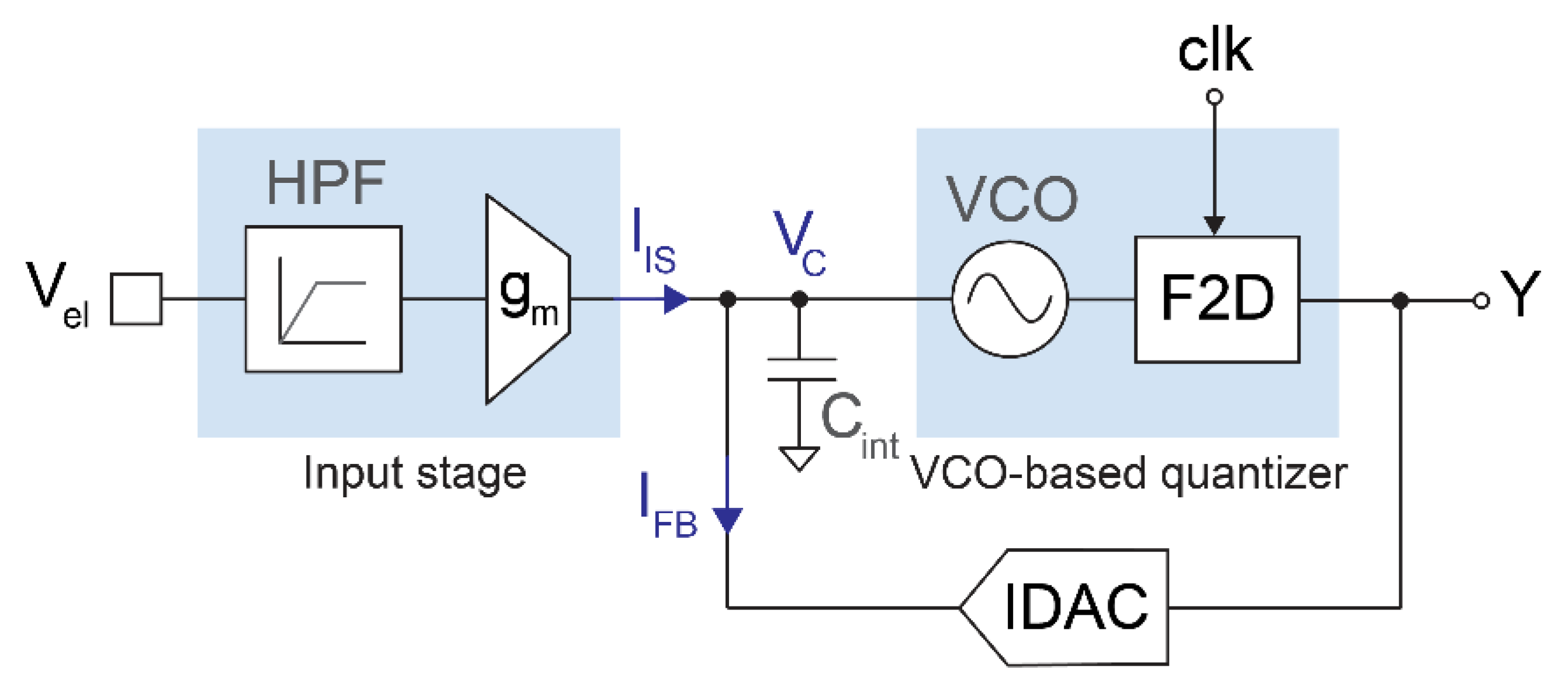
Figure 1 shows a simplified block diagram of the proposed readout circuit. The input stage transforms the electrode voltage (Vel) into a current (IIS) by means of a high-pass filter and an inverting transconductor. This current is injected into a capacitor (Cint), which acts as the first integrator of the modulator. The capacitor voltage (VC) drives a VCO-based quantizer consisting of a VCO and a 1-bit frequency-to-digital converter, which is sampled at 1 MHz. The output bitstream drives the 1-bit current DAC that generates the feedback current (IFB) and closes the loop. The modulator resembles a first-order closed-loop ∆Σ architecture with an opamp-less integrator, using a VCO-based quantizer to achieve an additional order of noise shaping [19,21]. The sampling frequency is high enough to achieve an input-referred quantization noise below 2 μVrms in the 300 Hz–6 kHz band with a 1-bit, second-order modulator, which keeps the structure of the converter very simple. Furthermore, the continuous-time topology obviates the need for an anti-aliasing filter due to the inherent low-pass filtering before sampling.
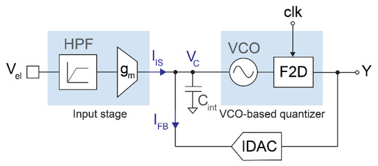
Figure 1.
Simplified block diagram of the proposed opamp-less, second-order ∆Σ modulator with VCO-based quantizer.
The modulator is stable, provided that the feedback current can rapidly counterbalance IIS for any possible input signal so that the average current through Cint is kept at zero. In normal operation, the capacitor voltage VC is an irregular triangular wave resembling the output of the first integrator of a continuous-time ∆Σ modulator. The average values of VC and Y are defined by the transfer functions of the feedback IDAC and the VCO-based quantizer. Under nominal conditions, () = () = 1.4 μA and () = VDD/2 = 0.9 V, which sets the average VCO oscillation frequency close to fs/2 = 500 kHz and = 0.5.
2.1. Input Stage
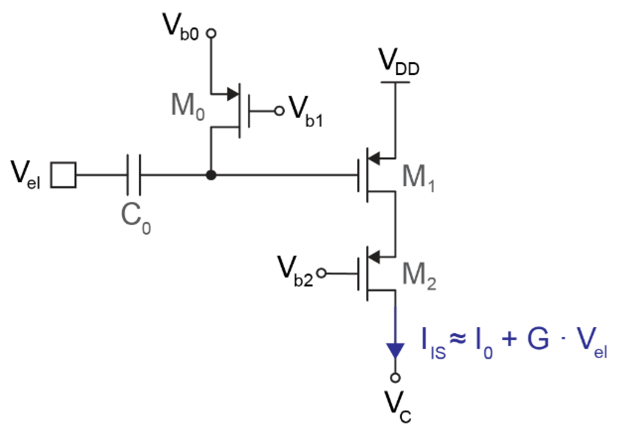
Figure 2 shows the schematic of the input stage, which consists of a high-pass filter followed by a single-ended transconductor. The high-pass filter is based on a metal–insulator–metal (MIM) capacitor (C0) and a PMOS pseudo-resistor (M0). C0 must be as large as possible since this capacitor forms a voltage divider with the input capacitance of the next stage (M1). However, given the relatively large size of MIM capacitors, the value of C0 is limited to either hundreds of femtofarads or a few picofarads, depending on the application. The modulator implemented can be programmed with either C0 = 4.25 pF (for full-band low-noise applications) or C0 = 350 fF (for compact action–potential readout).

Figure 2.
Schematic of the input stage, consisting of a high-pass filter (C0 and M0), a single PMOS transistor operating as transconductor (M1), and a cascode (M2).
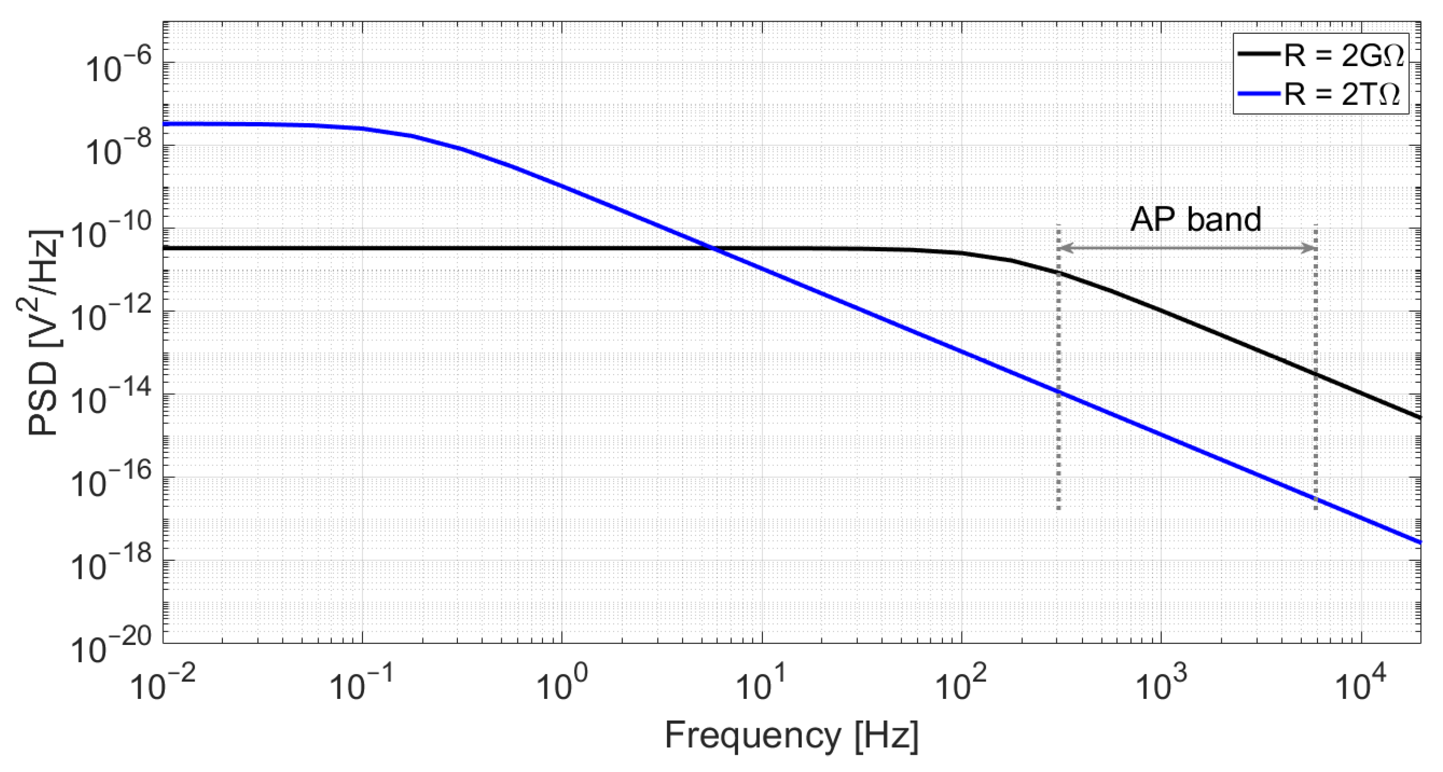
Given the small input capacitance, a very high-ohmic pseudo-resistor is needed to set the cut-off frequency of the high-pass filter well below 1 Hz. These filter characteristics are required to avoid signal attenuation or phase shifts in the band of interest but also to reduce the effect of the thermal noise generated by M0 since, as shown in Figure 3, the noise is low-pass-filtered by the RC circuit. As a consequence, the pseudo-resistor was tuned in the TΩ range.
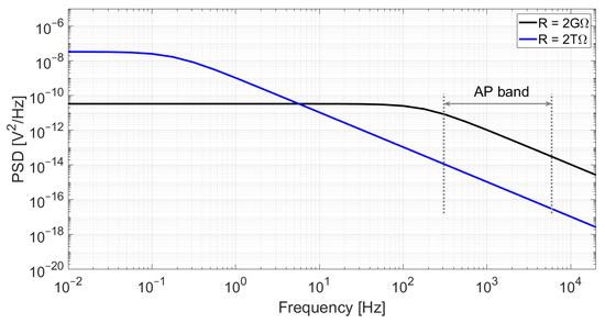
Figure 3.
Simulation of the output noise of an RC low-pass filter for C = 350 fF and two different resistor values: R = 2 GΩ (black) and R = 2 TΩ (blue). Although a higher resistance value yields higher power spectral density at low frequencies, the cut-off frequency is significantly reduced, which results in lower noise at high frequencies. In this example, the integrated noise in the action-potential band (300 Hz–6 kHz) is 58 μVrms for R = 2 GΩ and only 2.0 μVrms for R = 2 TΩ.
The transconductor is based on a single PMOS transistor (M1) in weak inversion. The main transistor is complemented with a cascode (M2) to increase the output impedance and keep the output current independent from the output voltage VC, which can oscillate up to ±200 mV around 900 mV. Assuming small input voltages, the current generated by this transconductor follows
where I0 is the DC biasing current, and G is the transconductance of M1 multiplied by the attenuation due to the capacitive voltage divider. The biasing current I0 chosen for all the measurements reported in this article is 1.4 μA, although the integrated circuit allows for tuning this current in the [200 nA, 1.6 μA] range to define different levels of power consumption and noise.
Two variants of this circuit have been implemented in the prototype chip: one optimized for compact neural interfaces and a second variant optimized for low noise. The compact transconductor is coupled to the 350 fF input capacitor and consists of M1 = 30 μm/1.2 μm and M2 = 10 μm/1.2 μm. The voltage divider, formed by the input capacitance (350 fF) and the gate capacitance of M1 (95 fF), attenuates the input signal by 2 dB and prevents the use of a larger transistor. The resulting transconductance of the input stage is G ≈ 20 V−1 · I0. The alternative low-noise transconductor is coupled to the 4.25 pF input transistor to avoid any signal attenuation in the capacitive voltage divider. Therefore, the size of M1 was increased up to 70 μm/1.5 μm (with M2 = 10 μm/1.5 μm), which reduces flicker noise at low frequencies. The resulting transconductance is G ≈ 25 V−1 · I0.
Although this transconductor topology is sensitive to power-supply noise and process variations, inverts the input signal, and is inherently nonlinear, it can be very compact and potentially feature low noise. Process variations can cause minor gain variations, which can be coped with through calibration. Nonlinearity may cause the distortion of very large input signals, but action potentials are expected to be smaller than 1 mV. The power-supply rejection ratio (PSRR) is nearly 0 dB since the output current directly depends on the VSG of M1 and, therefore, on the supply voltage. Low-noise external voltage regulators are required to minimize the power-supply noise, and data post-processing can be included to attenuate power-supply noise (50/60 Hz harmonics) and other types of predictable noise. Note that in the case of a MEA with multiple copies of the same converter, the power-supply noise is common to all of them, which makes the extraction and subtraction of common noise during data post-processing possible. The feasibility and robustness of compact, single-ended input stages for MEAs have also been recently proven in [12].
2.2. Feedback IDAC
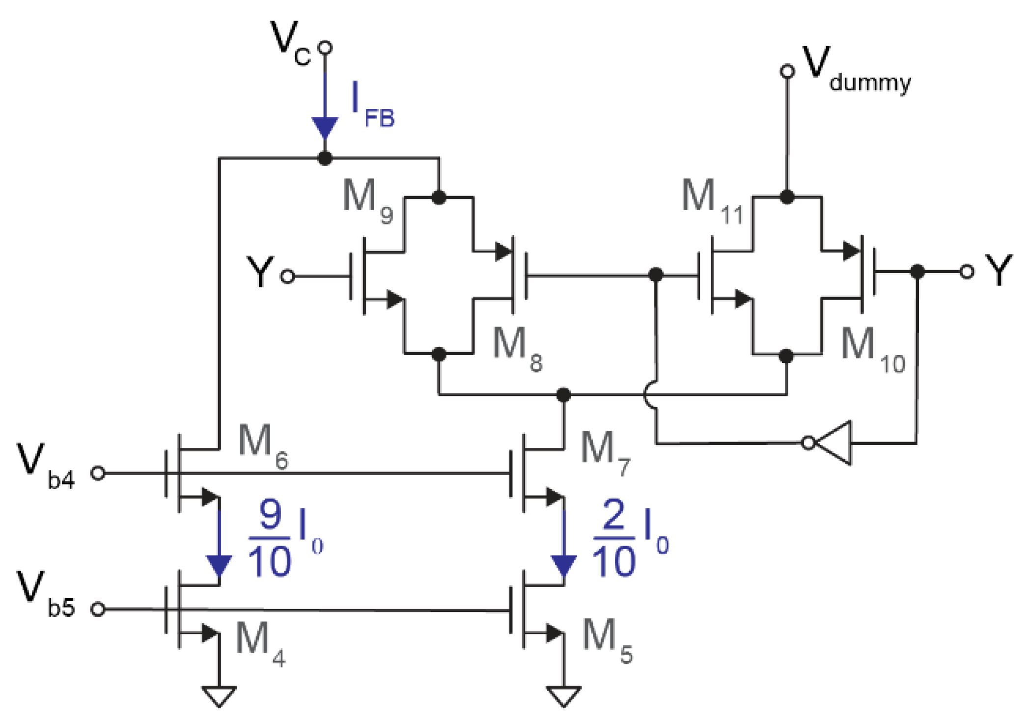
The current DAC consists of two current sources and two transmission gates. As shown in Figure 4, M4 and M6 generate IM4 = 0.9·I0 while M5 and M7 produce IM5 = 0.2·I0. Therefore, the instantaneous output current is
given that—depending on the feedback signal Y—transmission gates M8–M11 control whether the current IM5 is connected to VC, the output, through M8–M9 or discarded via M10–M11. As for the input stage, the biasing current I0 was fixed at 1.4 μA.
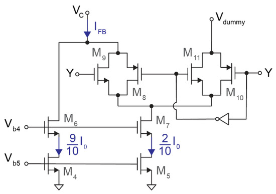
Figure 4.
Schematic of the 1-bit feedback IDAC. A first current source (M4) provides 0.9·I0 to the output, while the current generated by a second current source (M5) is injected into the output or discarded depending on the state of Y.
The modulator is stable only if any possible IIS current ranges between the two possible feedback currents. According to Equations (1) and (2), this condition is met if < 5 mV for C0 = 350 fF (G ≈ 20 V−1 · I0) and if < 4 mV for C0 = 4.25 pF (G ≈ 20 V−1 · I0). Nevertheless, the practically available full scale is considered to be 3 mVp in order to limit distortion and to avoid saturation and excessive quantization noise [22,23]. Moreover, this full-scale reduction relaxes requirements in terms of matching and robustness against process variations, since deviations from nominal parameters would not saturate the converter and could be corrected during digital-signal post-processing.
2.3. Integrator
The difference between input and feedback currents, IIS–IFB, flows through capacitor Cint, which acts as an integrator. The value of this capacitor defines the integration constant and, along with the biasing current and the voltage-controlled oscillator (VCO)-quantizer gain, the modulator transfer functions. The nominal capacitance for I0 = 1.4 μA is Cint = 775 fF, but a 5-bit programmable capacitor has been implemented to allow for capacitances from 25 fF to 775 fF in order to accommodate different biasing currents without significant changes in the state variable VC.
2.4. VCO-Based Quantizer
A VCO-based quantizer has been used to achieve second-order noise shaping without the need for a second analog integrator. The quantizer is the combination of a VCO whose frequency is modulated by voltage VC and a frequency-to-digital (F2D) converter whose output is a logic ‘1’ when a pulse from the VCO is detected during the preceding sampling period. A VCO-based quantizer can be modelled as a frequency integrator (the instantaneous VCO phase is the result of integrating the VCO frequency over time), followed by a phase quantizer and a discrete-time derivative [20,21]. The spectral properties of the resulting signal can be analyzed by modelling the VCO-based quantizer as a pulse–frequency modulator (PFM) [23].
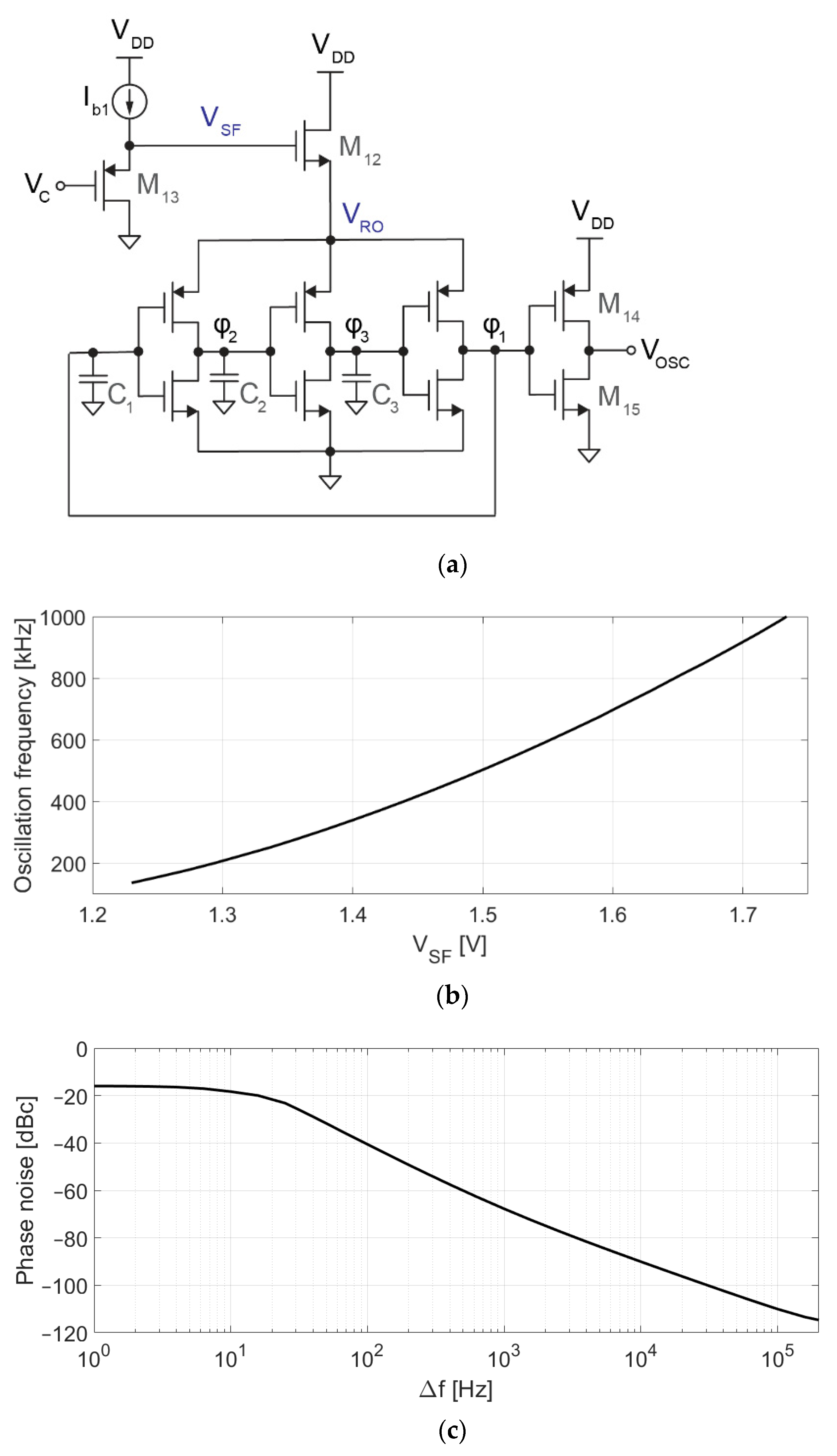
Figure 5a shows the schematic of the VCO. The core of this circuit is a 3-stage voltage-controlled ring oscillator, whose frequency depends on VSF, as shown in Figure 5b. For VSF = 1.5 V, the oscillation frequency and gain are fVCO = 500 kHz and KVCO = 1.6 kHz/mV with a current consumption of 250 nA. Transistor dimensions are 5 μm/6 μm for PMOS and 2 μm/6 μm for NMOS. Capacitors C1–C3 (70 fF) have been used to reduce the oscillation frequency, which would otherwise be too high or require too low of a current to bias M12. VRO is controlled by M12 (400 nm/20 μm), which acts as a source follower using the oscillator current for its own biasing. The gate of M12 cannot be directly driven by VC since the target (0.9 V) is lower than the target (1.5 V). M13 is a second source follower, used to adapt the DC level of VC to the 1.5 V required at VSF to set the oscillation frequency to around 500 kHz. Finally, M14 and M15 act as a level shifter, adapting the 620 mVpp oscillation at φ1 to the rail-to-rail levels demanded by digital circuitry.
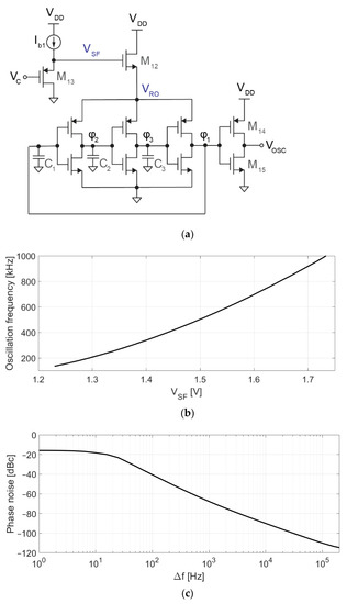
Figure 5.
Voltage-controlled oscillator. (a) Schematic of the VCO, consisting of a 3-stage ring oscillator, a level shifter (M14–M15), a source follower driving the ring oscillator (M12), and a second source follower (M13) for adapting the DC voltage level from VC (0.9 V) to VSF (1.5 V); (b) Simulated voltage-to-frequency response; (c) Simulated phase noise.
The proposed VCO is sensitive to process variations, and the exact relationship between the input voltage and the output frequency is difficult to predict. Fortunately, since the VCO operates in a closed-loop system, any deviation from the nominal behavior (e.g., the VCO being slower than expected at VC = 0.9 V) would be compensated by the loop (e.g., higher , correcting the average oscillation frequency). The VCO was optimized to minimize the impact of phase noise (shown in Figure 5c) and distortion in the performance of the converter [24], which is also mitigated by the closed-loop architecture. Time-domain simulations were used to verify that the performance of the modulator is not limited by phase noise or VCO distortion.
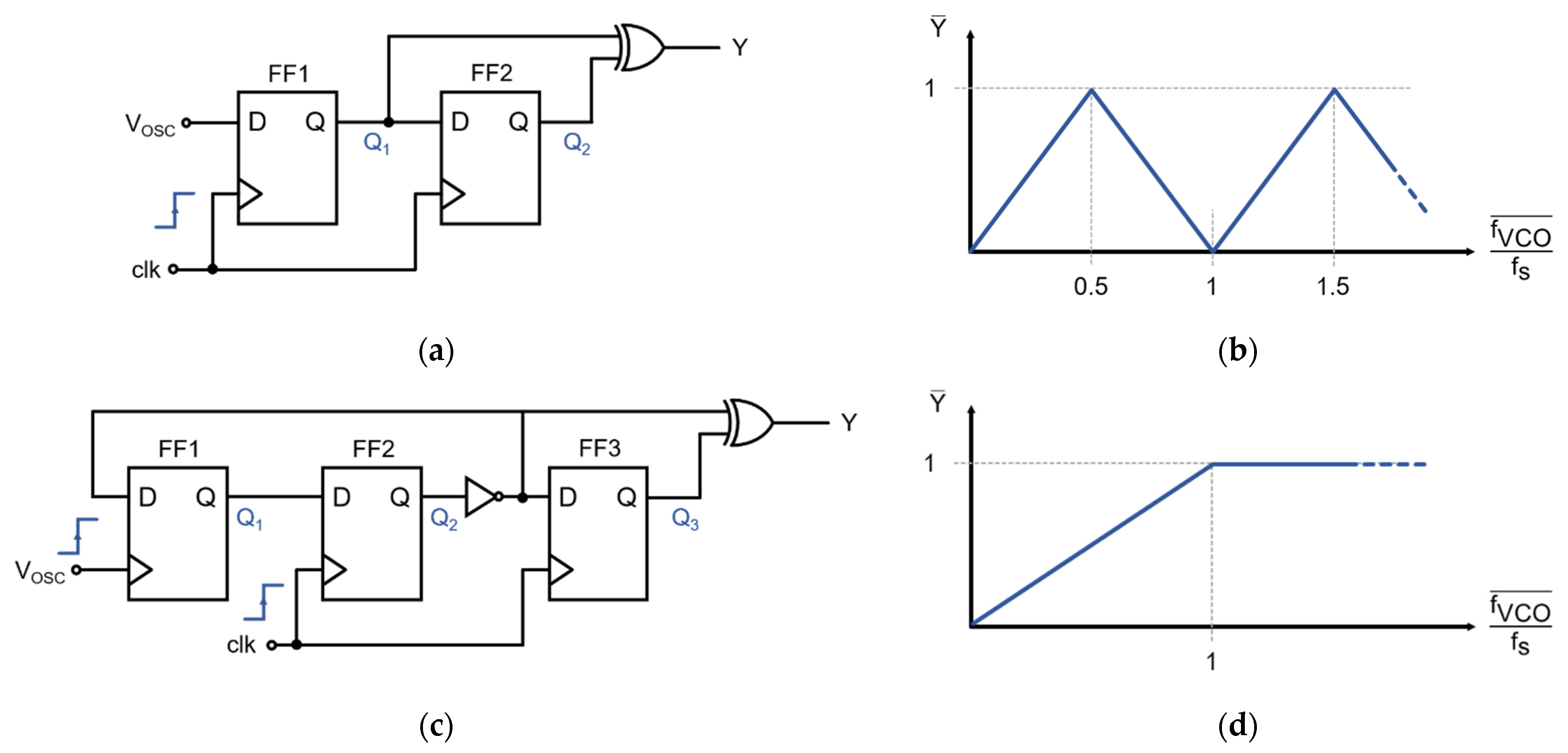
A frequency-to-digital converter is required to transform the asynchronous VCO oscillation into a synchronous pulse–frequency-modulated signal [21,23]. Figure 6a shows a classical F2D converter circuit that is based on two D-type flip-flops (FF) and an XOR-gate. Ideally, the output of this F2D is a logic ‘1’ if a VCO transition—either rising or falling—has been registered during the last sampling period. However, when transitions occur faster than the sampling frequency (i.e., fVCO > 0.5·fs), a fraction of the transitions is missed during sampling, and the frequency of the output pulses decreases for faster VCO frequencies. Figure 6b shows that the average output is a function of the normalized VCO frequency and that it is periodic. This F2D converter topology is frequently used in other modulator architectures for which the oscillation frequency is guaranteed to be lower than 0.5·fs. However, the closed-loop modulator presented in this work is intended to operate around ≈ 0.5·fs. The F2D converter of Figure 6a would not be suitable for this application since the modulator could find undesirable metastable operation points at higher oscillation frequencies, especially at ≈ 1.5·fs.
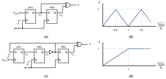
Figure 6.
Frequency-to-digital (F2D) converters. (a) Classical 2-flip-flop exclusive OR (XOR)-based frequency-to-digital converter; (b) Normalized frequency-to-digital response of the classical XOR-based F2D, which is not monotonic and may feature metastable states in the closed-loop converter; (c) Proposed frequency-to-digital converter, with a third flip-flop to force the saturation of the F2D; (d) Normalized frequency-to-digital response of the proposed F2D, which is monotonic and prevents metastable operating points.
The F2D converter used in this design is a variation of the classical exclusive OR (XOR)-based approach, depicted in Figure 6c. When the oscillation frequency is slower than the sampling frequency (i.e., for fVCO < fs), each pulse at VOSC toggles FF1, and this change is then registered by FF2, producing a logic ‘1’ at the output of the converter. When no pulses are received during a sampling period, Q3 = Q2, which renders Y = 0. For fVCO > fs, the F2D converter saturates, and the output is constantly ‘1’ since FF1 would toggle once every sampling period. This saturation at high frequencies, illustrated in Figure 6d, improves the stability of the system since only a specific range of frequencies around fs/2 is possible during normal operation.
3. Electrical Characterization
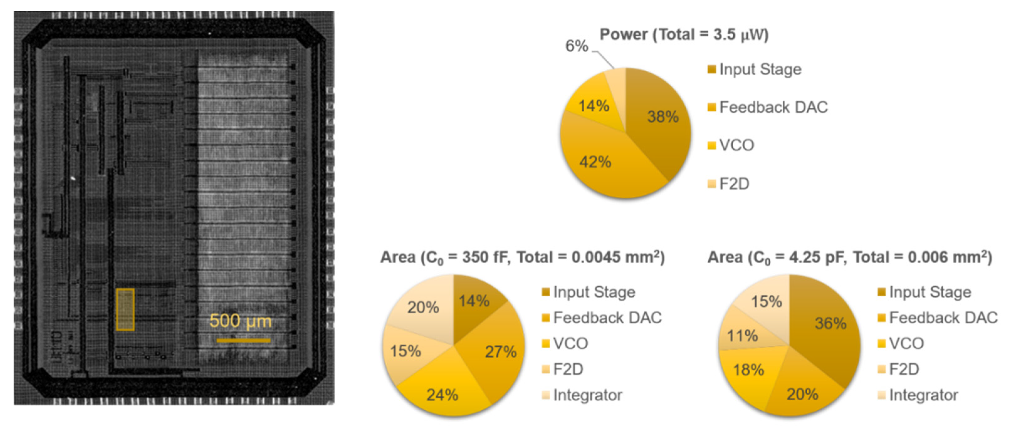
The proposed readout circuit has been prototyped in 0.18-μm CMOS technology (1P6M). Figure 7 shows the 3 × 3.8 mm2 chip, on which the highlighted 130 × 330 μm2 area was used for testing different ∆Σ configurations. Excluding the biasing and auxiliary circuitry required for testing, the building blocks of the compact modulator (C0 = 350 fF) occupied 0.0045 mm2, while the low-noise modulator occupied 0.006 mm2 due to the larger capacitor (C0 = 4.25 pF).

Figure 7.
Chip micrograph of the prototype fabricated in 0.18 μm CMOS, with the location of the system highlighted, and area and simulated power breakdowns.
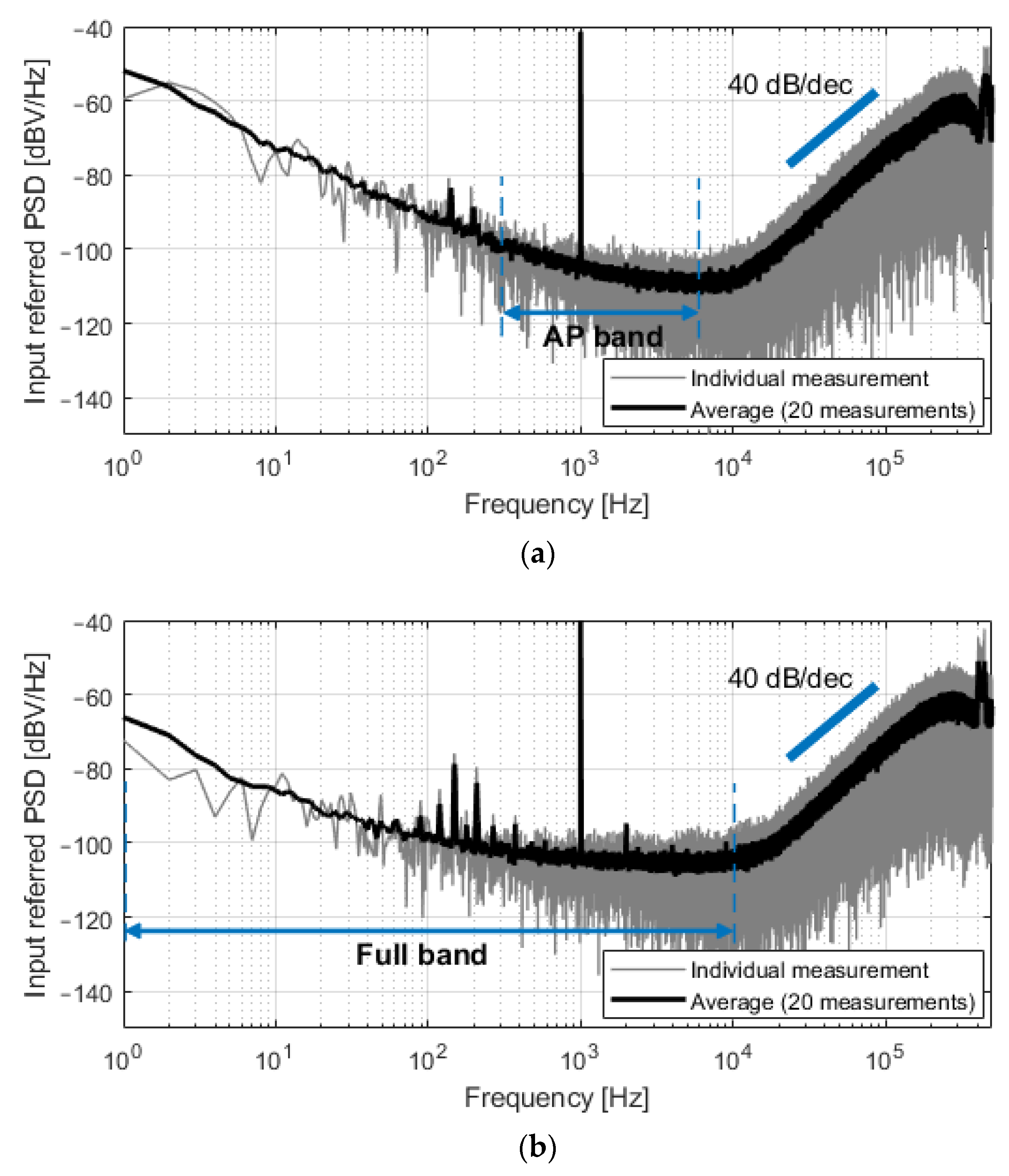
The system was first characterized by applying a 200 μVp sinusoidal input signal at 1 kHz. Figure 8 shows the spectra of the output bitstreams for both C0 = 350 fF and C0 = 4.25 pF. The spectrum in gray is the result of single measurements, while the black plot represents the average magnitude of 20 consecutive measurements. Second-order noise shaping is visible at high frequencies, and the input-referred noise was 5.0 μVrms in the 300 Hz–6 kHz band (C0 = 350 fF, Figure 8a) and 8.7 μVrms in the 1 Hz–10 kHz band (C0 = 4.25 pF, Figure 8b). Unexpected noise is present in the 80–500 Hz band and is especially visible in Figure 8b due to lower flicker noise. This noise is attributed to the measurement setup; however, its contribution to the total integrated in-band noise is minor.
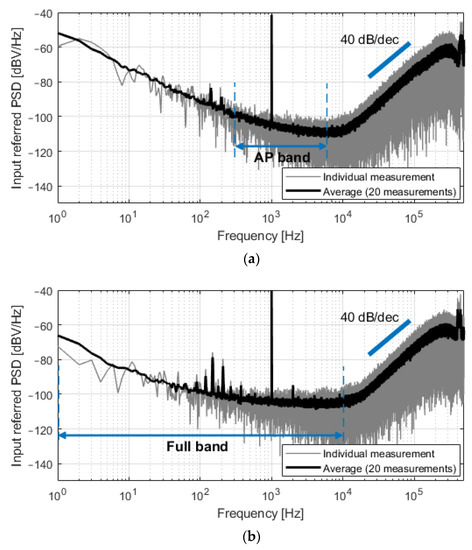
Figure 8.
Spectra of the measured output bitstreams, referred at the input of the converter, for a sinusoidal input of 200 μVp at 1 kHz. (a) For C0 = 350 fF, the input-referred noise in the 300 Hz–6 kHz band was 5.0 μVrms; (b) For C0 = 4.25 pF, the input-referred noise in the 1 Hz–10 kHz band was 8.7 μVrms.
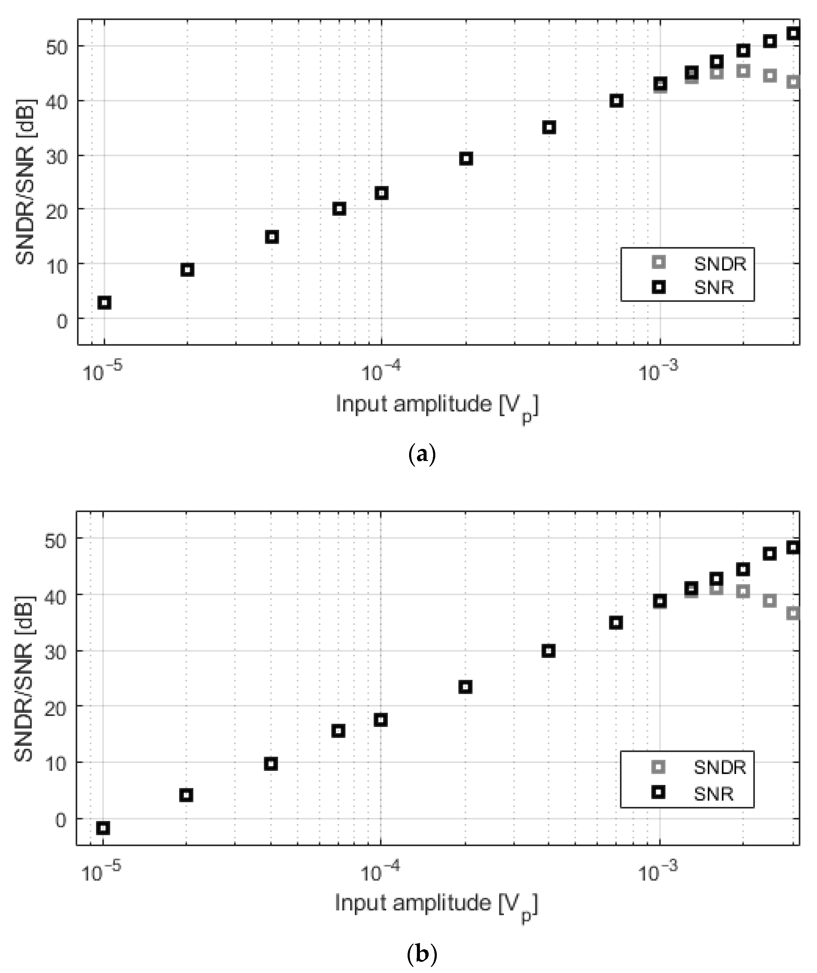
Figure 9 depicts the signal-to-noise ratio (SNR) and the signal-to-noise-and-distortion ratio (SNDR) for different input amplitudes at 1 kHz. Each point represents the average of 20 consecutive measurements. Signals larger than 1–1.5 mVp are limited by the distortion of the input-stage transconductor.
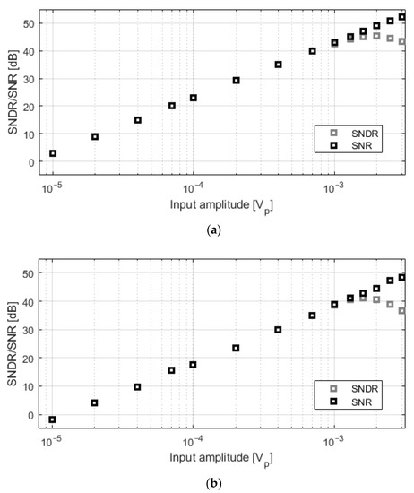
Figure 9.
Measured SNDR and SNR for different input amplitudes at 1 kHz. (a) C0 = 350 fF; (b) C0 = 4.25 pF.
The performance of the proposed readout is summarized in Table 1 and compared to the prior art, including readout circuits integrated into arrays for in vitro [3,9,11,12] platforms, in vivo implants [5,10,15,17], and standalone converters [13,16]. Our work features low noise characteristics (<6 μVrms), low power consumption (<5 μW/ch), and a compact footprint (<0.01 mm2/ch), which is in line with the state of the art. The overall performance of the converter presented in [13] appears superior; however, the converter reported here was implemented in 0.18-μm CMOS and provided synchronous output, which may be advantageous depending on the application. Finally, it is noteworthy that the converter reported in [17] achieves comparable metrics while it includes on-chip decimation filters.

Table 1.
Performance summary and comparison with state-of-the-art.
4. In Vitro Validation
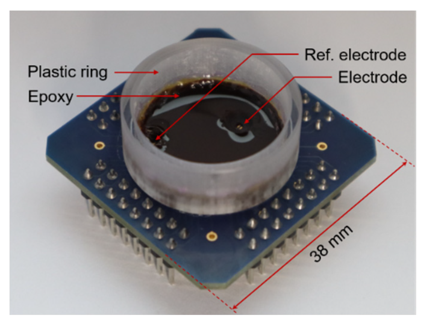
As a proof of concept, the implemented modulator was used to sense the field potentials of cardiac tissue. The CMOS prototype was wire-bonded to a custom-made PCB, where a 0.24 × 1.54 mm2 pad, covered with electroless nickel immersion gold (ENIG), was used as the electrode. Another ENIG electrode was used as a reference electrode and was connected to VDD = 1.8 V. As shown in Figure 10, a plastic ring was glued to the PCB, and the ASIC and bonding wires were covered with epoxy to leave only the selected electrodes exposed. These materials were selected in order to simplify the fabrication process and were stable enough for system characterization measurements but would not be suitable for long-term recordings.
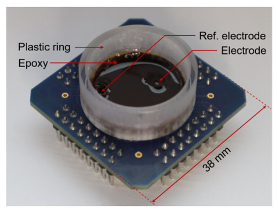
Figure 10.
Chip and package used for in vitro validation. The plastic ring defines the well by which cells and cell culture medium are confined during recordings. The bottom of the well is mainly covered with epoxy, with the exception of the electrode area.
The chip was cleaned and sterilized, and the electrodes were coated with human fibronectin to facilitate cell attachment. Human induced pluripotent stem cells (hIPSCs) derived from a healthy donor were purchased from FUJIFILM Cellular Dynamics Inc. The human induced pluripotent stem cell (hIPSC) line, CW30318CC1, was obtained from the CIRM hPSC Repository funded by the California Institute of Regenerative Medicine (CIRM). The hIPSCs were then differentiated into spontaneously and synchronously beating cardiomyocytes. The cardiomyocytes were carefully lifted from the cell culture dish to not disrupt the cell-cell connections. The cardiomyocyte tissue was then transferred and allowed to adhere to the surface with the coated electrodes.
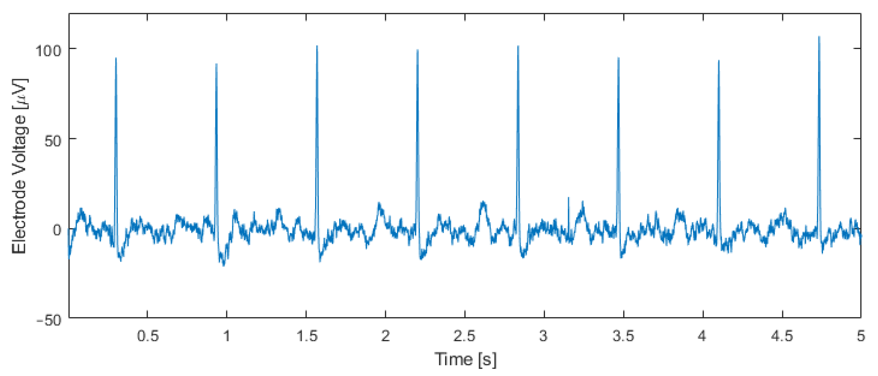
Figure 11 shows an electrical recording taken inside an incubator one hour after transferring the tissue to the chip. The input capacitor was set to C0 = 4.25 pF, and the output bitstream was band-pass filtered with a fourth-order Butterworth band-pass filter between 5 Hz and 200 Hz. Cardiac action potentials with an amplitude of approximately 100 μVpp and a beating rate of 95 beats per minute are visible. This beating rate matches the rate measured by observing the contractions of the tissue through the microscope.
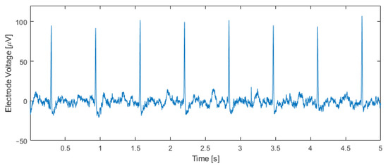
Figure 11.
Measurement results using human IPSC-derived cardiomyocytes. The output bitstream of the modulator (C0 = 4.25 pF) was band-pass filtered between 5 Hz and 200 Hz, unveiling cardiac potentials and a beating rate of 95 beats per minute, which matches the beating rate measured optically.
5. Conclusions
This paper proposes a readout circuit for bioelectrical signals based on a ∆Σ modulator with a VCO-based quantizer, which achieves second-order noise shaping with minimal analog circuitry. The size of the input capacitor plays a fundamental role in the design, as it defines the signal attenuation and the size of the input stage. A large P-type transistor serves as the input transconductor, which minimizes flicker noise without the need for chopping. Another capacitor was used for the integration of both input and feedback currents, eliminating the need for operational amplifiers. A novel frequency-to-digital converter was developed to improve the stability of the VCO-based quantization. The performance of the converter matches that of state-of-the-art devices in terms of noise, power, and area and constitutes a competitive solution for extracellular action–potential detection in large-scale electrode arrays and neural interfaces.
The resulting converter architecture is very simple and avoids conventional problems of more complex modulators, such as feedback DAC non-linearity. However, the proposed circuit is not inherently robust against power-supply noise, process variations, or input-stage non-linearity. Therefore, the modulator relies on low-noise external voltage regulators to minimize power-supply noise, and off-chip digital filtering can be used to attenuate noise at specific frequencies. Process variations may result in unexpected gain deviations, making calibration necessary if the absolute amplitude of signals is of interest. The non-linearity of the input stage can be neglected for small input signals, and distortion–compensation methods should be explored if large input signals are expected.
Author Contributions
Conceptualization, F.C.; circuit design, N.B. and F.C.; measurements, F.C. and J.L.; manuscript writing, F.C., N.B., J.L. and A.H.; funding acquisition, F.C. and A.H. All authors have read and agreed to the published version of the manuscript.
Funding
This work was supported by an ETH Postdoctoral Fellowship to F. Cardes, the European Research Council Advanced Grant 694829 ‘neuroXscales’ and the Swiss National Science Foundation project 205320_188910/1.
Acknowledgments
The authors would like to thank P. Rimpf, ETH Zurich, for chip packaging. N.B. would like to thank V. Valente, TU Delft, for his support and supervision.
Conflicts of Interest
The authors declare no conflict of interest.
References
- Hierlemann, A.; Frey, U.; Hafizovic, S.; Heer, F. Growing cells atop microelectronic chips: Interfacing electrogenic cells in vitro with CMOS-based microelectrode arrays. Proc. IEEE 2011, 99, 252–284. [Google Scholar] [CrossRef]
- Musk, E.; Neuralink. An integrated brain-machine interface platform with thousands of channels. J. Med. Internet Res. 2019, 21, 1–14. [Google Scholar] [CrossRef]
- Dragas, J.; Viswam, V.; Shadmani, A.; Chen, Y.; Bounik, R.; Stettler, A.; Radivojevic, M.; Geissler, S.; Obien, M.E.J.; Müller, J.; et al. In Vitro Multi-Functional Microelectrode Array Featuring 59760 Electrodes, 2048 Electrophysiology Channels, Stimulation, Impedance Measurement, and Neurotransmitter Detection Channels. IEEE J. Solid-State Circuits 2017, 52, 1576–1590. [Google Scholar] [CrossRef] [Green Version]
- Kollo, M.; Racz, R.; Hanna, M.E.; Obaid, A.; Angle, M.R.; Wray, W.; Kong, Y.; Müller, J.; Hierlemann, A.; Melosh, N.A.; et al. CHIME: CMOS-Hosted in vivo Microelectrodes for Massively Scalable Neuronal Recordings. Front. Neurosci. 2020, 14, 834. [Google Scholar] [CrossRef]
- Park, S.Y.; Cho, J.; Na, K.; Yoon, E. Modular 128-Channel Δ—ΔΣ Analog Front-End Architecture Using Spectrum Equalization Scheme for 1024-Channel 3-D Neural Recording Microsystems. IEEE J. Solid-State Circuits 2018, 53, 501–514. [Google Scholar] [CrossRef]
- Najafi, K.; Wise, K.D. An Implantable Multielectrode Array with On-Chip Signal Processing. IEEE J. Solid-State Circuits 1986, 21, 1035–1044. [Google Scholar] [CrossRef]
- Mora Lopez, C.; Putzeys, J.; Raducanu, B.C.; Ballini, M.; Wang, S.; Andrei, A.; Rochus, V.; Vandebriel, R.; Severi, S.; Van Hoof, C.; et al. A Neural Probe with Up to 966 Electrodes and Up to 384 Configurable Channels in 0.13 μm SOI CMOS. IEEE Trans. Biomed. Circuits Syst. 2017, 11, 510–522. [Google Scholar] [CrossRef] [Green Version]
- Rey, H.G.; Pedreira, C.; Quian Quiroga, R. Past, present and future of spike sorting techniques. Brain Res. Bull. 2015, 119, 106–117. [Google Scholar] [CrossRef] [Green Version]
- Kato, Y.; Matoba, Y.; Honda, K.; Ogawa, K.; Shimizu, K.; Maehara, M.; Fujiwara, A.; Odawara, A.; Yamane, C.; Kimizuka, N.; et al. High-Density and Large-Scale MEA System Featuring 236, 880 Electrodes at 11.72 μm Pitch for Neuronal Network Analysis. In Proceedings of the 2020 IEEE Symposium on VLSI Circuits, Honolulu, HI, USA, 16–19 June 2020; Volume 1, pp. 31–32. [Google Scholar] [CrossRef]
- Chang, S., II; Park, S.Y.; Yoon, E. Minimally-invasive neural interface for distributed wireless electrocorticogram recording systems. Sensors 2018, 18, 263. [Google Scholar] [CrossRef] [Green Version]
- Lopez, C.M.; Chun, H.S.; Wang, S.; Berti, L.; Putzeys, J.; Van Den Bulcke, C.; Weijers, J.W.; Firrincieli, A.; Reumers, V.; Braeken, D.; et al. A multimodal CMOS MEA for high-throughput intracellular action potential measurements and impedance spectroscopy in drug-screening applications. IEEE J. Solid-State Circuits 2018, 53, 3076–3086. [Google Scholar] [CrossRef]
- Yuan, X.; Hierlemann, A.; Frey, U. Extracellular Recording of Entire Neural Networks Using a Dual-Mode Microelectrode Array with 19 584 Electrodes and High SNR. IEEE J. Solid-State Circuits 2021, 56, 2466–2475. [Google Scholar] [CrossRef] [PubMed]
- Leene, L.B.; Constandinou, T.G. A 0.006 mm2 1.2 μ W Analog-to-Time Converter for Asynchronous Bio-Sensors. IEEE J. Solid-State Circuits 2018, 53, 2604–2613. [Google Scholar] [CrossRef]
- Ballini, M.; Muller, J.; Livi, P.; Chen, Y.; Frey, U.; Stettler, A.; Shadmani, A.; Viswam, V.; Lloyd Jones, I.; Jackel, D.; et al. A 1024-Channel CMOS Microelectrode Array with 26,400 Electrodes for Recording and Stimulation of Electrogenic Cells In Vitro. IEEE J. Solid-State Circuits 2014, 49, 2705–2719. [Google Scholar] [CrossRef] [Green Version]
- Lee, C.; Jeon, T.; Jang, M.; Park, S.; Kim, J.; Lim, J.; Ahn, J.; Huh, Y.; Chae, Y. A 6.5-μW 10-kHz BW 80.4-dB SNDR Gm C-Based CT Modulator with a Feedback-Assisted Gm Linearization for Artifact-Tolerant. IEEE J. Solid-State Circuits 2020, 55, 2889–2901. [Google Scholar] [CrossRef]
- Pazhouhandeh, M.R.; Kassiri, H.; Shoukry, A.; Weisspapir, I.; Carlen, P.L.; Genov, R. Opamp-Less Sub-μW/Channel Delta-Modulated Neural-ADC with Super-G Input Impedance. IEEE J. Solid-State Circuits 2021, 56, 1565–1575. [Google Scholar] [CrossRef]
- Wendler, D.; De Dorigo, D.; Amayreh, M.; Bleitner, A.; Marx, M.; Manoli, Y. A 0.00378 mm2 Scalable Neural Recording Front-End for Fully Immersible Neural Probes Based on a Two-Step Incremental Delta-Sigma Converter with Extended Counting and Hardware Reuse. In Proceedings of the 2021 IEEE International Solid-State Circuits Conference (ISSCC), San Francisco, CA, USA, 13–22 February 2021; Volume 64, pp. 398–400. [Google Scholar] [CrossRef]
- Schreier, R.; Temes, G.C. Understanding Delta-Sigma Data Converters; Wiley-IEEE Press: Hoboken, NJ, USA, 2005; ISBN 9780471465850. [Google Scholar]
- Park, M.; Perrott, M.H. A 78 dB SNDR 87 mW 20 MHz Bandwidth Continuous-Time DS ADC with VCO-Based Integrator and Quantizer Implemented in 0.13 μm CMOS. IEEE J. Solid-State Circuits 2009, 44, 3344–3358. [Google Scholar] [CrossRef]
- Straayer, M.Z.; Perrott, M.H. A 12-Bit, 10-MHz Bandwidth, Continuous-Time SD ADC with a 5-Bit, 950-MS/s VCO-Based Quantizer. IEEE J. Solid-State Circuits 2008, 43, 805–814. [Google Scholar] [CrossRef]
- Kim, J.; Jang, T.K.; Yoon, Y.G.; Cho, S.H. Analysis and design of voltage-controlled oscillator based analog-to-digital converter. IEEE Trans. Circuits Syst. I Regul. Pap. 2010, 57, 18–30. [Google Scholar] [CrossRef]
- Ardalan, S.H.; Paulos, J.J. An Analysis of Nonlinear Behavior in Delta-Sigma Modulators. IEEE Trans. Cir. Syst. 1987, 34, 593–603. [Google Scholar] [CrossRef]
- Gutierrez, E.; Hernandez, L.; Cardes, F.; Rombouts, P. A Pulse Frequency Modulation Interpretation of VCOs Enabling VCO-ADC Architectures with Extended Noise Shaping. IEEE Trans. Circuits Syst. I Regul. Pap. 2018, 65, 444–457. [Google Scholar] [CrossRef]
- Cardes, F.; Quintero, A.; Gutierrez, E.; Buffa, C.; Wiesbauer, A.; Hernandez, L. SNDR limits of oscillator-based sensor readout circuits. Sensors 2018, 18, 445. [Google Scholar] [CrossRef] [PubMed] [Green Version]
Publisher’s Note: MDPI stays neutral with regard to jurisdictional claims in published maps and institutional affiliations. |
© 2021 by the authors. Licensee MDPI, Basel, Switzerland. This article is an open access article distributed under the terms and conditions of the Creative Commons Attribution (CC BY) license (https://creativecommons.org/licenses/by/4.0/).