Article

Modeling and Optimization of a Novel ScAlN-Based MEMS Scanning Mirror with Large Static and Dynamic Two-Axis Tilting Angles

1
School of Electronics and Information, Yangtze University, Jingzhou 434023, China
2
Cooperative Innovation Center of Unconventional Oil and Gas, Yangtze University, Ministry of Education, Wuhan 430100, China
3
Key Laboratory of Optoelectronic Technology & Systems, Chongqing University, Ministry of Education, Chongqing 400044, China
4
State Key Laboratory of Transducer Technology, Shanghai Institute of Microsystem and Information Technology, Chinese Academy of Sciences, Shanghai 200050, China
*
Author to whom correspondence should be addressed.
Sensors 2021, 21(16), 5513; https://doi.org/10.3390/s21165513
Submission received: 2 July 2021 / Revised: 3 August 2021 / Accepted: 10 August 2021 / Published: 17 August 2021
(This article belongs to the Section Physical Sensors)

Abstract

:
The piezoelectric MEMS (micro-electro-mechanical systems) scanning mirrors are in a great demand for numerous optoelectronic applications. However, the existing actuation strategies are severely limited for poor compatibility with CMOS process, non-linear control, insufficient mirror size and small angular travel. In this paper, a novel, particularly efficient ScAlN-based piezoelectric MEMS mirror with a pupil size of 10 mm is presented. The MEMS mirror consists of a reflection mirror plate, four meandering springs with mechanical rotation transformation, and eight right-angle trapezoidal actuators designed in Union Jack-shaped form. Theoretical modeling, simulations and comparative analysis have been investigated for optimizing two different device designs. For Device A with a 1 mm-length square mirror, the orthogonal and diagonal static tilting angles are ±36.2°@200 VDC and ±36.2°@180 VDC, respectively, and the dynamic tilting angles increases linearly with the driving voltage. Device B with a 10 mm-length square mirror provides the accessible tilting angles of ±36.0°@200 VDC and ±35.9°@180 VDC for horizontal and diagonal actuations, respectively. In the dynamic actuation regime, the orthogonal and diagonal tilting angles at 10 Hz are ±8.1°/Vpp and ±8.9°/Vpp, respectively. This work confirmed that the Union Jack-shaped arrangement of trapezoidal actuators is a promising option for designing powerful optical devices.

1. Introduction

Micro-electro-mechanical systems (MEMS)-based scanning mirrors have been proven as an indispensable technology in laser radar [1], optical communication [2], optical switches [3], high-resolution displays [4] and biomedical imaging [5]. The main advantages of MEMS scanning mirrors over the conventional large-size mechanisms include: miniaturized structure, low-power consumption, easy integration and cost efficiency. Typically, a reliable MEMS scanning mirror, for instance used in light detection and ranging (LIDAR) imaging [1], is desired to provide a specified tilting angle and retain its position at arbitrary moment according to the applied voltage. Moreover, the ideal scanning mirror should have good mechanical linearity (>99%), high-accuracy control in the range above ±15° and a pupil size of 1 mm to 10 mm to achieve high resolution [1,6,7,8,9,10,11]. Until now, there have been a variety of actuation methods for MEMS scanning mirrors, mostly based on electrostatic, electromagnetic, electrothermal and piezoelectric actuation principles [12,13,14,15,16].
Owing to simple implementation, easy process integration and low power consumption, the electrostatic actuation has become a relatively mature method. The electrostatic actuator for MEMS scanning mirrors is essentially a capacitor with two parallel plates to produce the electrostatic force and then drive the mirror plate oscillation. Considering the fact that the parallel plate actuation force is proportional to the square of the voltage, a high voltage of several hundred volts is typically applied to target a large effective deflection and tilting angle. However, the pull-in phenomenon, which always occurs in the central region of the parallel plates under high voltage excitation, not only requires a strict compromise between the effective plate deflection and the driving voltage, but it also brings micromirror failure risk. Meanwhile, the electrostatic force with a non-linear relationship to its applied voltage undoubtedly makes the micromirror control complicated. To address this issue, some vertical electrostatic comb-drive actuators have been designed [10,17,18], while the complexities of the device structure and microfabrication process limit their practical applications. As one of the alternatives, the electromagnetic actuation based on the Lorentz force is also frequently adopted due to the large deflection at a low driving voltage and a high scanning frequency up to 15 kHz. The defects of this mechanism include high power consumption, complex microfabrication process and unidirectional actuation with regard to the soft magnetic micromirrors [1,14,19]. Li et al. developed a polymer composite-based hard-magnetic micromirror with bidirectional rotation, but the deflection angle of the micromirror ranges only between ±1.3° [20]. The electrothermal actuation is another important method for actuating MEMS scanning mirrors, which possesses good linear control performance and large deflection angle. Nevertheless, its intrinsic thermal dissipation, slow response, long-term instability and relatively high power consumption has made this option less attractive for implementation in portable and large array applications [19].
Although each actuation method above can exhibit some unique characteristics for certain applications, some common challenges confronted largely prevent the achievement of both large 2-degrees-of-freedom (2-DoF) tilting angles and static non-resonant operation. In comparison, numerous impressive piezoelectric actuation micromirrors reported in the previous literature have demonstrated the achievement of resonant/static actuation mode, linear control, fast response and low power consumption characteristics [4,11,16,21,22,23,24]. A piezoelectric micromirror is less affected by air damping, thermal or electromagnetic interference than those driven by the electrostatic, thermal or electromagnetic force. Besides the advantages in the actuation mechanisms, a wide variety of designs for piezoelectric MEMS mirrors have also been developed, with most of them deploying a large mechanical rotation angle and a low operation voltage level [4,11,16,22,23,24]. Such superior architectures are almost entirely based on bulk or thin PbZrxTi1−xO3 (PZT) piezoelectric material to meet the requirements in laser projection and detection applications. For instance, Baran et al. developed a 1.4 mm-wide PZT thin-film actuation scanning mirror with the combination of mechanical amplification, exhibiting an optical scan angle of 38.5° at 24 V with the resonant frequency of 40 kHz [4]. Chen et al. presents a MEMS thin-PZT cantilever driven micro-lens actuator capable of delivering a large out-of-plane displacement of 145 μm at 22 V driving voltage, with a resonant frequency of 2 kHz [16]. Although commonly used PZT-type micromirrors exhibit large deflection due to high piezoelectric coefficients, the high permittivity resulting in low energy conversion efficiency, large temperature coefficient, low Curie point, hysteresis behavior, challengeable patterning process and poor compatibility with the mainstream complementary metal-oxide-semiconductor (CMOS) and/or MEMS process greatly limits its wide use in the MEMS area [4,20,21,22,23,24].
The AlN-based piezoelectric actuation strategy for a micromirror application has been presented and fabricated firstly by Shao et al., with a modified silicon-on-insulator-based MEMS process, demonstrating full CMOS compatibility, excellent linear control and various mirror movement modes [21]. However, both dynamic and static mirror operation modes of this device have the tilting angles of only about 0.2°/V and 0.005°/V, respectively, which is attributed to low piezoelectric coefficients of AlN material. Besides, a similar AlN-based micromirror with a larger aperture has also been developed [25], while its static analysis shows a very low mechanical rotation efficiency owing to the under-optimized actuator design. Based on Table 1, ScAlN, as a significantly higher performance piezoelectric material than AlN and PZT, can be used to deliver a large mechanical tilting angle of ±14° at 150 VDC [11,26,27], in addition to the aforementioned inherent superiorities in AlN-based micromirrors. Although only a handful of ScAlN-based micromirrors have been created with the improvement of piezoelectric coefficient e 31 , f [11,28,29,30], almost all of them have a limited mirror plate with the aperture size of less than 1 mm. Generally, the large aperture size and mass of a MEMS scanning mirror limits the possibility of achieving a larger scanning angle and a higher operation frequency unless the actuation moment is high enough [9]. Up to now, to overcome the aforementioned limitations of PZT-, AlN- and ScAlN-based micromirrors, a MEMS scanning mirror with two-dimensional static and/or dynamic tilting angles of greater than ±15° in the centimeter range is desired and being pursued for laser projection applications [11,31]. In addition to improving the fabricate uniformity with low residual stress, raising the piezoelectric coefficient of ScAlN material and deploying multiple ScAlN layers, one of the most pressing areas of research needed to significantly promote MEMS mirror technology lies primarily in pushing novel advanced designs.
Aiming at further improving the theoretical scanning angle of the ScAlN-based MEMS mirror, a novel actuation mechanism with large two-axis tilting angles at both static and dynamic operation modes is developed in this paper. The structural description and operation principle of the actuator will be detailed in Section 2. The analytical modeling and analysis is presented in Section 3. The three-dimensional (3D) finite-element modeling (FEM) simulation and optimization is investigated and discussed in Section 4, followed by conclusions in Section 5.

2. Electromechanical Design of ScAlN-Based Piezoelectric Micro-Electro-Mechanical Systems (MEMS) Mirror

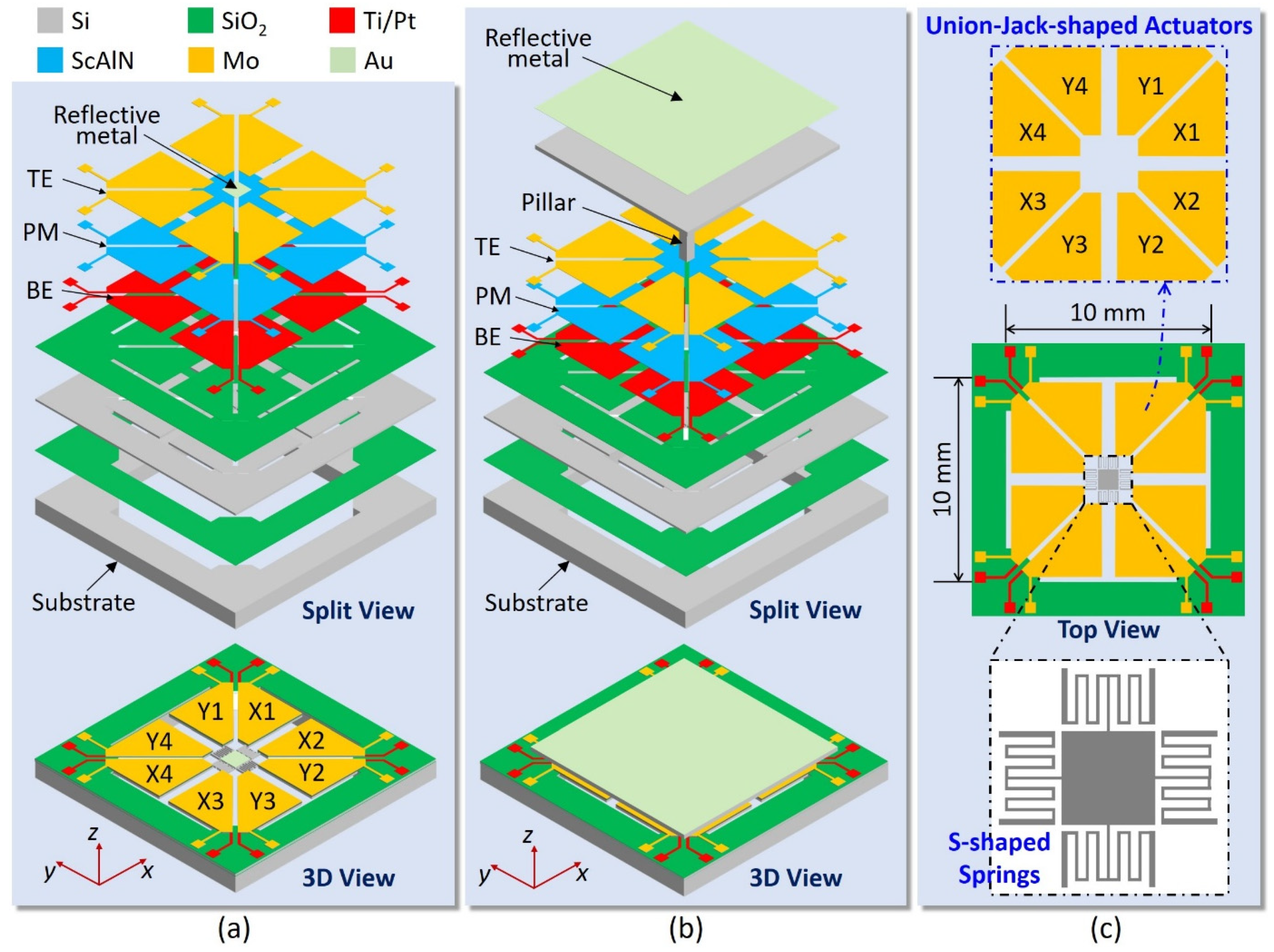
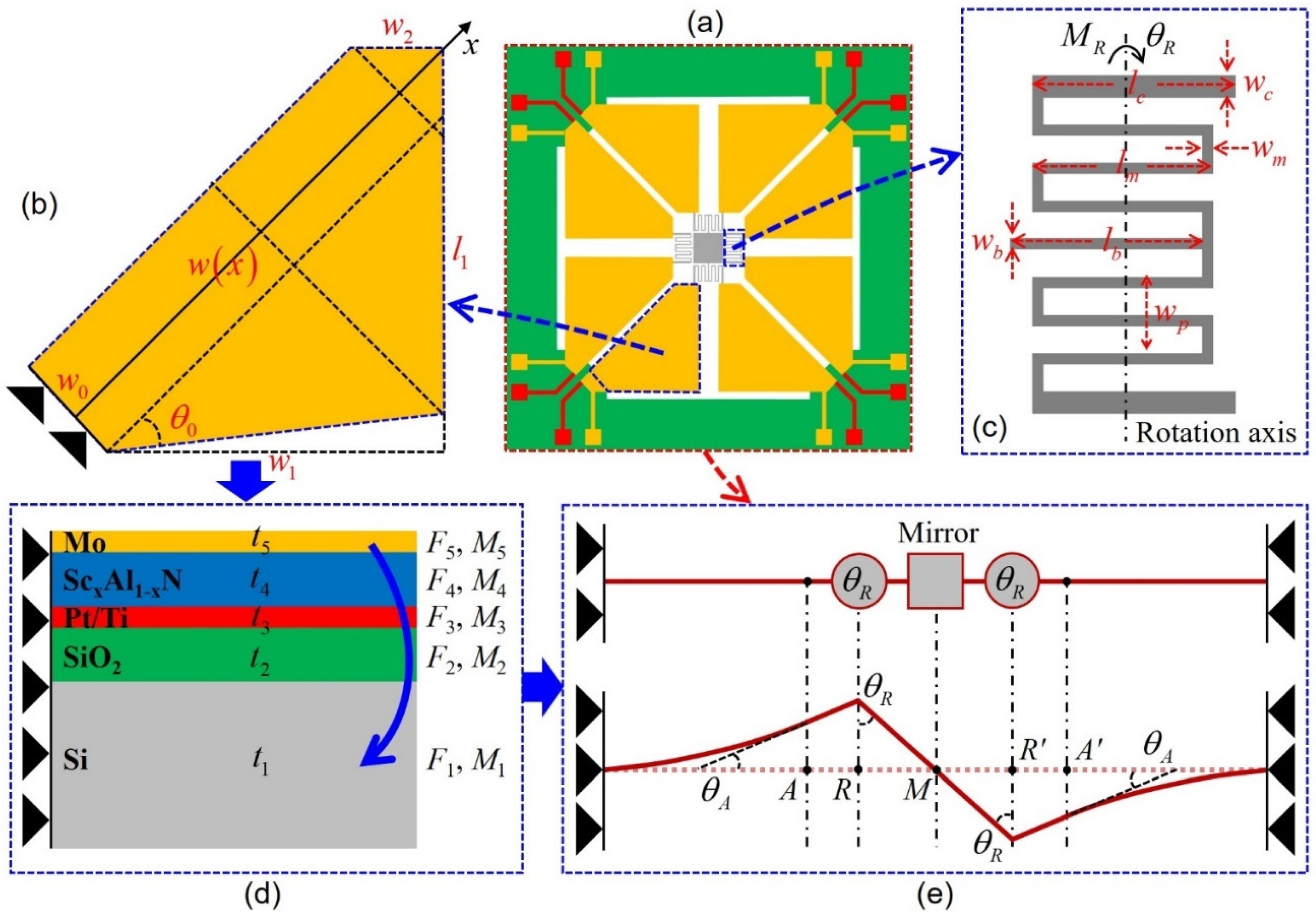
2.1. MEMS Mirror Structure

Due to the aforementioned factors, a particularly efficient piezoelectric MEMS scanning mirror has been designed for investigating both the static and dynamic electromechanical performance using ScxAl1−xN material as the actuator with Sc content up to x = 0.50. As illustrated in Figure 1, the architecture of the MEMS mirror (Device A) is composed of a square reflection mirror plate and eight trapezoidal ScxAl1−xN-based piezoelectric microcantilevers (PMs) sandwiched between a 200 nm top electrode (TE) and a 200 nm bottom electrode (BE), which are connected to a silicon-on-insulator (SOI) substrate having a 10-μm-thick device layer. Both the insulating SiO2 layer and ScxAl1−xN film have the thickness of 1 μm. The mirror plate is coated with 150 nm Au thin film to increase the reflective coefficient of the reflector. To explore a much larger mechanical tilting angle than ±15° within 150 V DC voltage, eight PMs are arranged as Union Jack-shaped actuators and four S-shaped meandering springs are adopted to connect the actuators and the mirror plate (referring to Figure 1c). Such spring design can not only avoid high stress concentrations in the corners, but also leverage its rotation transformation to enlarge the tilting angle of the MEMS mirror. Benefiting from this MEMS mirror design, good mode separation without crosstalk is more easily achieved when operating at dynamic resonance mode, especially at multiple resonance modes.
To further satisfy the light manipulation requirements from laser radar and vision science applications for an effective mirror region of roughly 10 × 10 mm2, a modified MEMS mirror design concept (Device B) based on Device A is presented in Figure 1b, where a square pillar is placed on the central holding platform driven by eight PM actuators to mechanically support the square mirror plate with a length of 10 mm and a thickness of 100 μm. The height of the pillar is determined by the maximum tilting angle, i.e., it must be set at above 2.4 mm to target 25° tilting angle. Note that the maximum principal stress within both devices A and B need be controlled at the level of 800 MPa to ensure no mechanical failure [4,11,33]. The geometrical parameter specifications of the proposed MEMS mirror devices A and B have been listed in Table 2.

2.2. Actuation Principle

When the driving voltages of PM actuators are distributed in an axisymmetric form, the induced actuation force applied on the proposed MEMS mirror will appear in pairs with opposite directions, resulting in antisymmetric deflections on two opposite sides of the MEMS mirror and a tilting rotation motion along its symmetrical axis. The main difference between these new mirror designs (A, B) and previously developed structures lies in the actuation principle: eight trapezoidal ScxAl1−xN based PM actuators are fully deployed as bendable microcantilevers to efficiently deliver the bending forces and moments for arbitrary two-axis rotation motions of the MEMS mirror. The separate actuators design has also beneficial influence on the structure stiffness to adjust the dynamic resonance frequency of the mirror. The other advantage of such trapezoidal PM actuator design is to enlarge the effective actuation length of the microcantilever within the same device frame by fixing the actuator corners instead of their straight edges parallel to x or y axes. Based on COMSOL simulations, Figure 2 shows the mirror actuation principle for some targeted tilting angles (0°, 45°, 90° and 135°) in the cases of using only four PM actuators and all eight PM actuators. Although both two actuation cases are able to achieve arbitrary tilting angles, the eight PM actuators arrangement turns out to be more efficient from the aspect of the deflection, which can improve the output performance by about 50%.

3. Modeling and Analysis

For the designed MEMS mirrors, analytical modeling of the trapezoidal ScxAl1−xN based actuators is essential to better understand their scanning characteristics and optimize the structural parameters. The static deflection and tilting angle at the bias voltage excitations are key performance indices to represent the device sensitivity. In the following mathematical models, each actuator is approximately modeled as a multilayer microcantilever with a fixed boundary condition at one end and a roller boundary condition at the meandering spring connection end, as shown in Figure 3, where the S-shaped meandering springs are functionalized as the rotation transformer. What needs illustration before modeling is that the right-angled trapezoidal actuators in Figure 4 are in a final designed form after optimization of structural angle θ0 (i.e., θ0 = 45°). In addition, to simplify the calculations, it is assumed that the initial residual stress caused during the microfabrication can be ignored and the radius of curvature resulting from the applied bending force is much larger than the total thickness of the multilayer trapezoidal actuator. Each layer of the actuator is in static equilibrium and the ScxAl1−xN piezoelectric layer has already been polarized during theoretical analysis.

3.1. Analytical Model of the Static Behavior Multilayer Trapezoidal Actuator

The basic geometry of a multilayer trapezoidal actuator is illustrated in Figure 3. Such an actuator is comprised of one piezoelectric layer and four purely elastic layers, as a result, the conventional model of only single-layer piezoelectric actuator is not valid here.
According to the force and moment equilibrium conditions of the multilayer actuator, the total force F t o t a l and moment M t o t a l can be expressed as:
F t o t a l = i = 1 5 F i = 0
M t o t a l = i = 1 5 M i + i = 1 5 F i ( j = 1 i 1 t j + t i 2 ) = 0
where t 0 = 0 , t i is the thickness of the i-th layer in the multilayer actuator, F i and M i are the force and moment at the cross section of the i-th layer shown in Figure 3d, respectively. According to the assumption that the actuator thickness is much less than the overall actuator curvature, the curvature R of each layer is approximately equal to each other, which can be given by [34]:
1 R = i = 1 5 M i / i = 1 5 C i
C i = 1 3 E i w ( x ) t i [ t i 2 + 3 ( z n j = 1 i t j ) ( z n j = 1 i 1 t j ) ]
w ( x ) = { w 0 + x tan θ 0 , x 2 w 1 / ( 1 + tan θ 0 ) w 0 + 2 w 1 x , x w 0 + 2 ( w 1 w 2 ) 2 w 0 + 2 ( 2 w 1 w 2 ) 2 x , x L 0
where Ei and Ci represents the Young’s modulus and flexural rigidity of the i-th layer in the multilayer actuator, respectively, and L 0 = w 0 + 2 ( w 1 w 2 / 2 ) is the effective actuation length of the multilayer actuator. The effective surface area of the actuator can be obtained by integrating its width w(x) along the length direction x, which is proportional to the structural angle θ0 and reaches the maximum at θ0 = 45°. As a result, the flexural rigidity Ci of the i-th layer has a maximum value when θ0 = 45°. zn is the neutral axis position, which is calculated according to:
z n = 2 i = 1 5 E i t i j = 1 i t j i = 1 5 E i t i 2 2 i = 1 5 E i t i
The bending moments produced in the multilayer actuator contains two part: one moment M4 produced in the piezoelectric layer and one opposing moment MR associated to the torsional meandering spring. To model the deflection and bending angle of the piezoelectric actuator for the static operation case, we can firstly assume the bending angle at one spring connecting end of the piezoelectric layer is given as θA and the angle at the other end of the torsional meandering spring is estimated as θR under the torque MR. Therefore, the bending moment of the multilayer actuator is the difference between these two moments, given by:
i = 1 5 M i = M 4 M R = E 4 w ( x ) d 31 p t 4 V ( z n j = 1 4 t j + t 4 2 ) M R
M R = K θ R ( π 2 θ A + θ R )
where KθR is the torsional spring constant, which is equal to the spring constant of all meandering spring segments in series.
Insertion of Equations (4) and (7) into (3) yields:
1 R = 3 E 4 d 31 p t 4 V ( z n j = 1 4 t j + t 4 2 ) i = 1 5 E i t i [ t i 2 + 3 ( z n j = 1 i t j ) ( z n j = 1 i 1 t j ) ] K θ R ( π 2 θ A + θ R ) i = 1 5 C i
Equation (9) shows that the structural angle θ0 should be optimized at 45° to obtain the best defection performance, which is highly consistent with the following simulated results. In order to derive KθR about the rotation axis with a flexural rigidity CR1 of each horizontal spring segment and CR2 of each vertical spring segment, it can be summarized as the following [16]:
1 K θ R = 8 w p w m C R 1 + 6 l m + 2 l c C R 2
Combining Equations (9) and (10), the deflection ξ ( x ) of the actuator along the x-axis, in relation to the curvature R, is written as:
ξ ( x ) = x 2 2 R , 0 x L 0
The bending angle θ(x) of the actuator can be yielded for small deflections as:
θ ( x ) = d ξ ( x ) d x = x R , 0 x L 0
Considering that the bending angle θ(x) at the tip deflection of the actuator equals θA, the rotation angle θR of the meandering spring should meet the following relationship:
θ R = arcsin [ ξ ( L 0 ) + ( l c l m / 2 ) sin θ A l b l m / 2 ]
Therefore, the statically driven mirror rotation angle θR for arbitrary DC voltage excitation can be calculated and optimized by means of integration of Equations (9)–(12) according to (13), which is a function of structural parameters of the multilayer trapezoidal actuator.

3.2. Analytical Model of the Dynamic Behavior Multilayer Trapezoidal Actuator

In addition to the static behavior of the multilayer trapezoidal actuator, the analytical prediction of its dynamic behavior is also of significance. When the multilayer trapezoidal actuator operates at the bending vibration eigenmodes with the damping ra, the differential equation for bending motions of the actuator with the external load f(x,t) can be given by:
C 4 ξ ( x , t ) x 4 + μ 2 ξ ( x , t ) t 2 + r a ξ ( x , t ) t = f ( x , t )
where ξ ( x , t ) = ξ ( x ) ϕ ( t ) = m = 1 ξ m ( x ) ϕ m e j ω m t which absolutely converges as m increases to , C = i = 1 5 C i represents the total flexural rigidity over the length direction of the actuator, ω m physically corresponds to the m-th natural bending vibration mode, μ is defined as follows:
μ = i = 1 5 ρ i t i w ( x )
The general solution ξ ( x ) of Equation (14) results from the fixed-roller boundary conditions of the multilayer trapezoidal actuator, which are represented by:
ξ ( 0 ) = 0 , d ξ ( 0 ) d x = 0
d 2 ξ ( L 0 ) d x 2 = M 4 M R C , d 3 ξ ( L 0 ) d x 3 = M R C ( l b l m / 2 )
The m-th natural vibration mode frequency of the actuator can be determined by:
ω m = a m 2 L 0 2 C μ
where a m denotes the characteristic zeros of the m-th natural vibration mode.
In combination with Equations (16) and (17), the deflection ξ m ( x ) of the m-th natural vibration mode can be determined by adopting the linearly independent Rayleigh functions for solving Equation (14) [35]:
ξ m ( x ) = 1 2 [ cosh ( a m x L 0 ) cos ( a m x L 0 ) ] 1 2 b m [ sinh ( a m x L 0 ) sin ( a m x L 0 ) ]
where b m is defined by:
b m = cosh ( a m ) + cos ( a m ) sinh ( a m ) + sin ( a m )
Taking the orthogonality properties for bending waves arising on the bending actuator into account, multiplication on both sides of Equation (14) with ξ m ( x ) and following integration with respect to the actuator length L 0 results in [10]:
ϕ ¨ m + 2 ς m ω m ϕ ˙ m + ω m 2 ϕ m = 0 L 0 f ( x , t ) ξ m ( x ) d x μ 0 L 0 ξ m 2 ( x ) d x
where r a / μ = 2 ς m ω m , ς m denotes a dimensionless attenuation constant. Equation (21) determines the temporal characteristics of the bending vibration eigenmode ξ m ( x ) taking the damping r a into consideration.
The mechanical stresses originate from the piezoelectric layer and are referred to as piezoelectric moment M4 in accordance with Equation (7). The harmonic driving voltage V(t) is applied over the whole piezoelectric bending actuator, thus the resulting load f(x,t) can be defined by the Dirac delta function, written as:
f ( x , t ) = M 4 cos ( Ω t ) [ d δ d x ( x L 0 ) d δ d x ( x ) ]
In combination with the fixed-roller boundary conditions and Equation (22), Equation (21) results in:
ϕ ¨ m + 2 ς m ω m ϕ ˙ m + ω m 2 ϕ m = M 4 cos ( Ω t ) ξ ( L 0 ) μ 0 L 0 ξ m 2 ( x ) d x
Since the attenuation constant ς m is different from zero, the homogeneous solution decays in time. After expiration of the transient time, the oscillation ϕ m ( t ) yields the particular solution:
ϕ m ( t ) = ξ ( L 0 ) ω m 2 μ 0 L 0 ξ m 2 ( x ) d x ( 1 Ω 2 / ω m 2 ) 2 + ( 2 ς m Ω / ω m ) 2 M 4 cos ( Ω t ψ m )
where the quantity denotes the phase angle in accordance with:
tan ψ m = 2 ς m Ω / ω m 1 Ω 2 / ω m 2
Thus, the spatial and temporal deflection of the piezoelectric bending actuator yields:
ξ ( x , t ) = m = 1 ξ ( x ) ξ ( L 0 ) ω m 2 μ 0 L 0 ξ m 2 ( x ) d x ( 1 Ω 2 / ω m 2 ) 2 + ( 2 ς m Ω / ω m ) 2 M 4 cos ( Ω t ψ m )
By means of differentiation of the deflection ξ ( x , t ) with respect to x, the bending angle θ A ( t ) at the tip of the piezoelectric actuator results in:
θ A ( t ) = m = 1 [ ξ ( L 0 ) ] 2 ω m 2 μ 0 L 0 ξ m 2 ( x ) d x ( 1 Ω 2 / ω m 2 ) 2 + ( 2 ς m Ω / ω m ) 2 M 4 cos ( Ω t ψ m )
In combination with Equation (13), the dynamically driven mirror rotation angle θR(t) for a harmonic voltage excitation can be predicted.

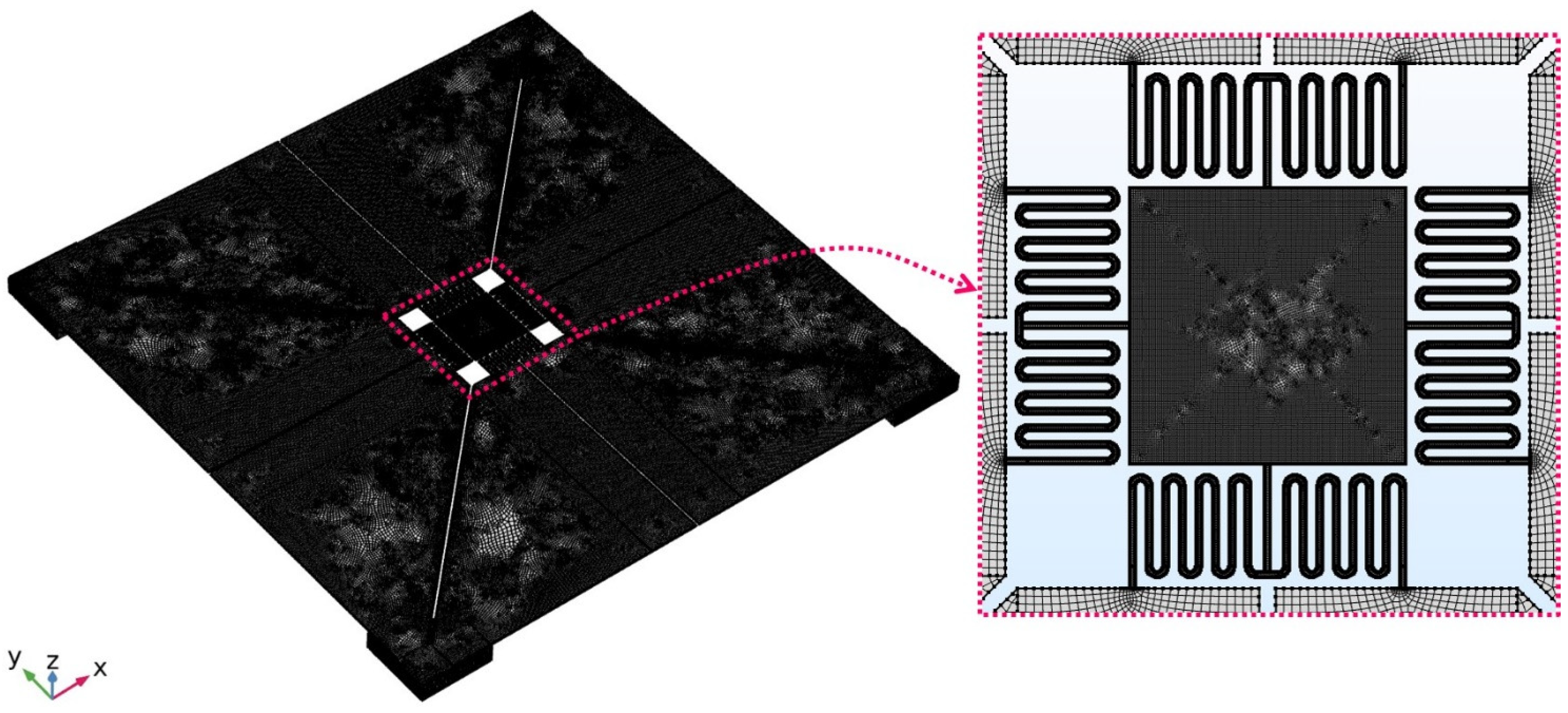
4. Three-Dimensional (3D) Finite-Element Modeling (FEM) Simulation, Optimization and Discussion

To better understand the static and dynamic characteristics of the proposed devices A and B, 3D FEM analysis and optimization were performed using Multiphysics COMSOL commercial simulation software. The mechanical and piezoelectric properties of the ScxAl1−xN layer with the Sc content x ranging from 0% to 50% can be approximately predicted by the following Equations (28) and (29) [27,36,37,38], while the material properties of the other layers used in the simulations are listed in Table 3. It is noted that both the mechanical damping and dielectric loss within the ScxAl1−xN layer have been considered as 0.01 during simulations in view of actual conditions [11,26,37]. The meshing of the entire geometry has been taken by the sweep mesh with the quadrilateral source faces, as depicted in Figure 4. The number of domain elements is about 0.5 million with the maximum and average growth rates of roughly 3.4 and 1.1, respectively. The number of degrees of freedom solved for the model is about 9 million. Besides, the fixed boundaries at the lower surfaces of the silicon substrate are used for the FEM models. The relative tolerance during the simulation studies is set at 0.01 to balance the computation speed and accuracy.
C 11 ( x ) = 410.2 ( 1 x ) + 295.3 x 210.3 x ( 1 x ) C 12 ( x ) = 142.4 ( 1 x ) + 198.6 x 61.9 x ( 1 x ) C 13 ( x ) = 110.1 ( 1 x ) + 135.5 x + 78.9 x ( 1 x ) C 33 ( x ) = 385 ( 1 x ) 23.8 x 101.4 x ( 1 x ) C 44 ( x ) = 122.9 ( 1 x ) + 169.5 x 137.3 x ( 1 x ) C 66 ( x ) = 0.5 C 11 ( x ) 0.5 C 12 ( x )
d 15 ( x ) = 3.17 + 0.487 x + 0.660 x 2 0.746 x 3 d 31 ( x ) = 2.14 15.09 x + 78.8 x 2 229 x 3 d 33 ( x ) = 5.02 + 42.3 x 238 x 2 + 704 x 3

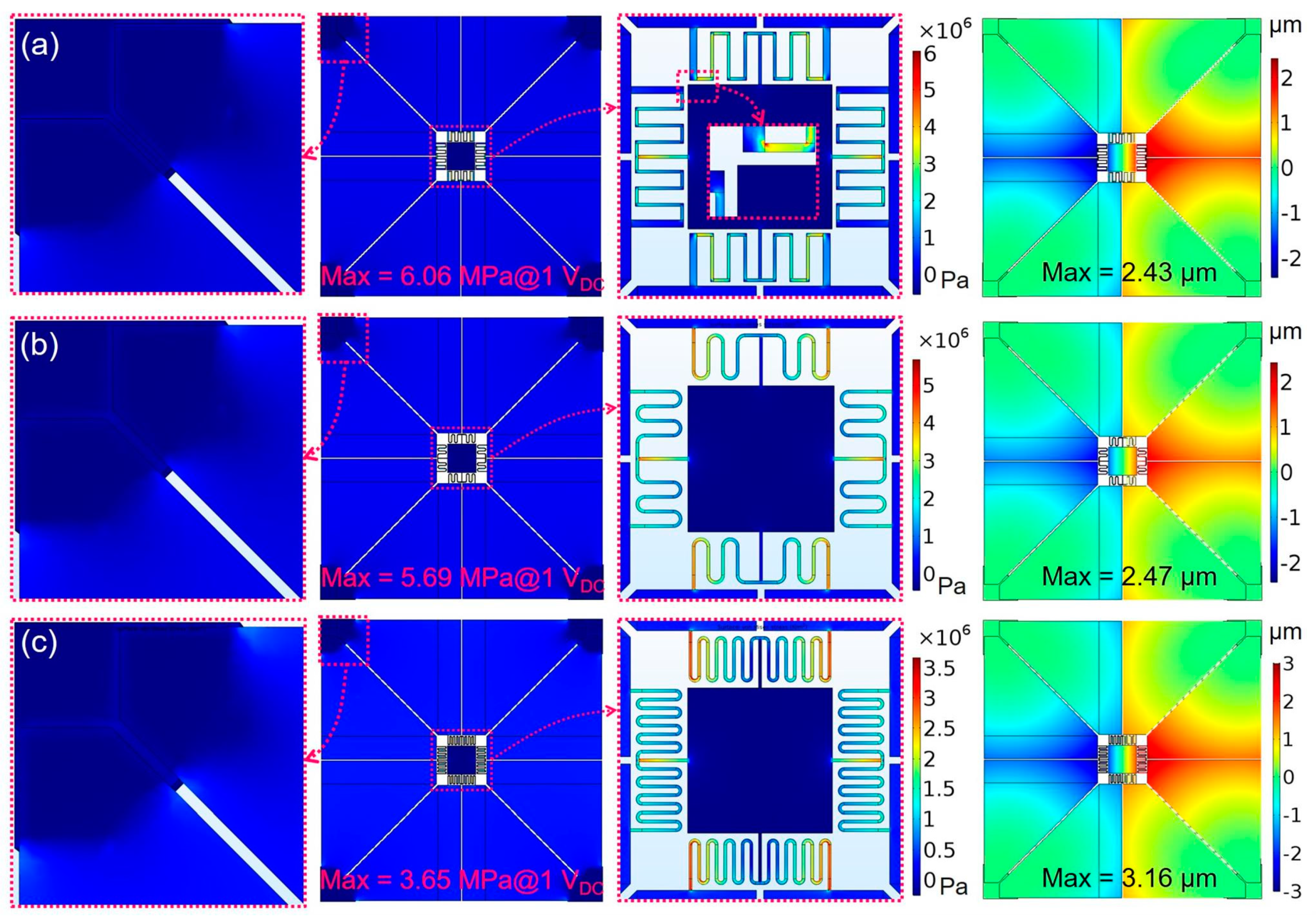
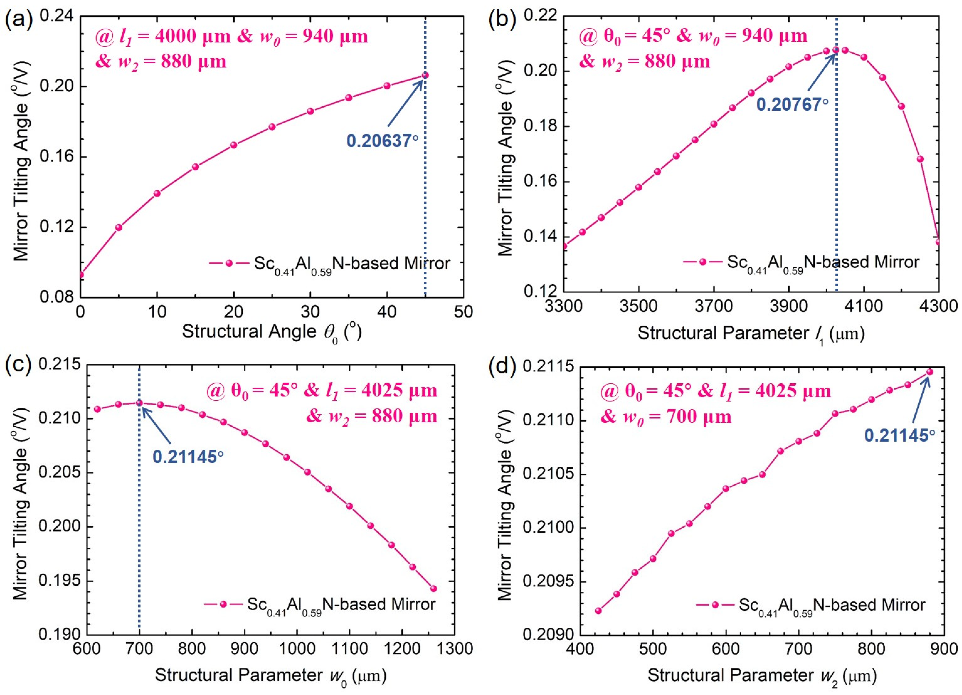
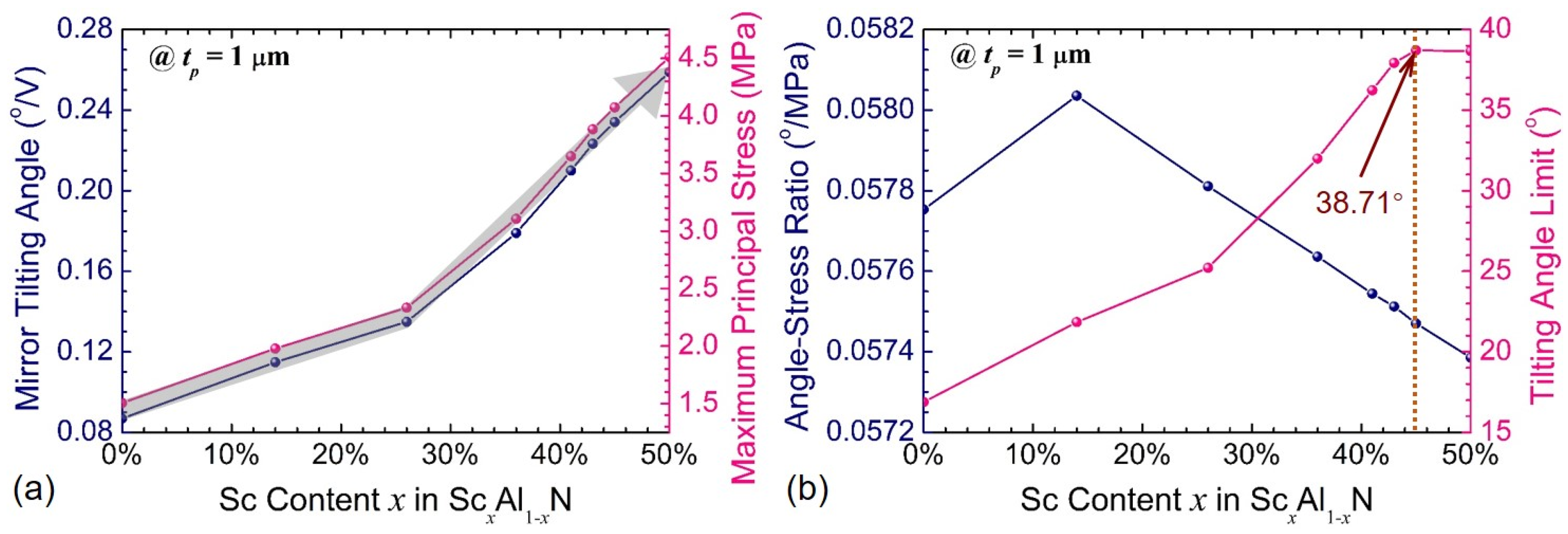
4.1. Structure Optimization

In order to achieve a static tilting angle of greater than ±15°, the piezoelectric MEMS mirror is typically required to be driven at a DC voltage up to 200 V, which will increase the risk of the device failure notably due to the maximum material stress beyond the break strength for the Si layer. The reachable tilting angles of the proposed Devices A and B are restricted by the stress limit of the materials. To avoid any breaking down behavior, maximum principal stress of less than 800 MPa is expected, in other words, the maximum principal stress per 1 VDC voltage should be no higher than 4.0 MPa. Therefore, the first structural optimization point is the maximum principal stress within the piezoelectric MEMS mirror. Accordingly, FEM simulations at 1 VDC voltage were performed for three different meandering spring designs, as shown in Figure 5. Note that the Sc content in ScxAl1−xN film is assumed as 41% which has been processed and tested to provide a piezoelectric coefficient e 31 , f of about 2.83 C/m2 in several previous works of literature [27,32,37,38]. By comparing the results, it is obviously demonstrated that the S-shaped meandering springs in Figure 5b,c have less maximum principal stress than the rectangular-shaped meandering spring in Figure 5a. In addition, the maximum principal stress can be further reduced and the maximum mechanical deflection can be improved to some extent by properly decreasing the spring pitch and increasing the number of the spring turns. The S-shaped meandering spring design in Figure 5c has been adopted in all subsequent simulations.
The second structural optimization point is for the piezoelectric MEMS actuator, which plays an important role in improving the reachable tilting angles. Based on the theoretical Equations (11)–(13), the mirror rotation angle θR depends critically on the structural parameters θ0, l1, w0 and w2 which are independent and irrelevant to each other. Thus, these four structural parameters can be optimized individually by using a control variate method with three out of four structural parameters fixed for each parametric sweep. According to the simulation results shown in Figure 6, the structural angle θ0 of the multilayer trapezoidal actuator is optimized at 45° when l1 = 4000 μm, w0 = 940 μm and w2 = 880 μm, defining the actuator as right-angled trapezoidal shape, which is highly consistent with the above theoretical analysis. Moreover, there is a peak value for both the structural parameters l1 and w0. After further optimizing structural parameter w2 in its range, it can be seen from Figure 6d that the static tilting angle of the MEMS mirror reaches the threshold value of 0.21145°/VDC. The optimal values of structural parameters l1, w0 and w2 are given in Table 2.
The thickness of the piezoelectric film and Si device layer is another important structural parameter to determine the mechanical tilting angle and frequency response. With increasing the thickness ts of the Si device layer, it is demonstrated from simulation results shown in Figure 7 that the MEMS scanning mirror will deliver a smaller mechanical tilting angle and linearly increase resonance frequencies for both piston modes and tilt modes. To obtain a more powerful ScxAl1−xN-based scanning mirror from the perspective of structural design, deploying a thicker ScxAl1−xN film to reduce electrical field intensity and induced stress may be an alternative approach [11]. The mechanical tilting angles and maximum principal stress of the MEMS scanning mirrors with 1 μm-thick and 2 μm-thick Sc0.41Al0.59N films are shown in Figure 7a,b. The tilting angle ratio Rtp is defined as the ratio of the mirror tilting angles of two device designs with 1 μm-thick and 2 μm-thick Sc0.41Al0.59N films. The tilting angle ratio Rtp increases with the thickness of the Si device layer and can be improved by about 20% when the thickness of the Si device layer is larger than 20 μm. The simulation results indicate that a 2 μm-thick Sc0.41Al0.59N based mirror can work more efficiently than a 1 μm-thick Sc0.41Al0.59N based mirror only when the thickness of the Si device layer is not less than 10 μm, because the thickness of Sc0.41Al0.59N film will make a significant impact on the total flexural rigidity of the multilayer actuator when the Si device layer is too thin, thereby affecting the mechanical deflection and tilting angle. Thus the thickness of the Sc0.41Al0.59N and Si device layers are set as 1 μm and 10 μm in all subsequent simulations, respectively.
In addition to the optimization of the structural parameters, the influence of the Sc content in ScxAl1−xN film on the mechanical efficiency of the MEMS scanning mirror has also been considered. As shown in Figure 8a, both the mechanical tilting angle and maximum principal stress increases piecewise linearly with the Sc content changing from 0% to 50%. Considering the limitations that the maximum principal stress and driving DC voltage of the designed mirrors should be controlled within 800 MPa and 200 VDC [16], respectively, it is necessary to strike a better balance between them in order to achieve its full potential. The ratio of the tilting angle and maximum principal stress for ScxAl1−xN -based mirrors with different Sc contents is defined to demonstrate the sensitivity to the material stress, as shown in Figure 8b. By analyzing the attainable tilting angle subject to the above limitations, it is suggested that the best performance of the designed mirror may be realized when the Sc content in ScxAl1−xN film increases to 45~50%. However, according to the previously reported experiments in terms of ScAlN crystal structure and piezoelectric response [36,37,38,41], both hexagonal wurtzite and cubic rocksalt phases coexist when the Sc content is between 42% and 45% and the crystal orientation drastically decreases when the Sc content is above 45%, implying that the optimal value of the Sc content in the proposed ScxAl1−xN-based mirrors is within range of 41~45%. Moreover, the manufacturing process for achieving the scandium concentration of higher than 42% is really challenging in the present studies. Alternatively, the Sc content of 41% is considered in all subsequent simulations to further investigate both the static and dynamic performance of the designed mirrors.

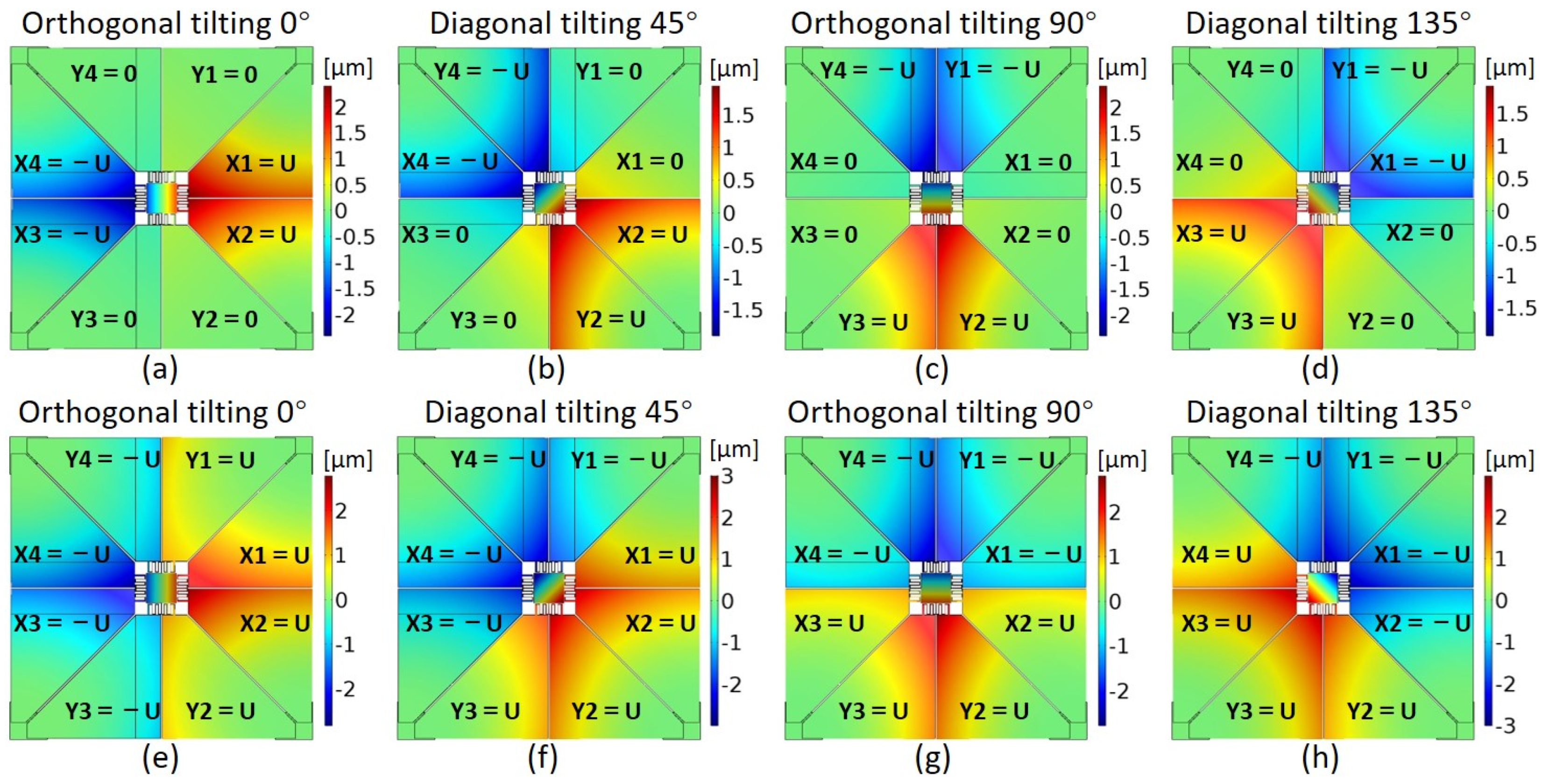
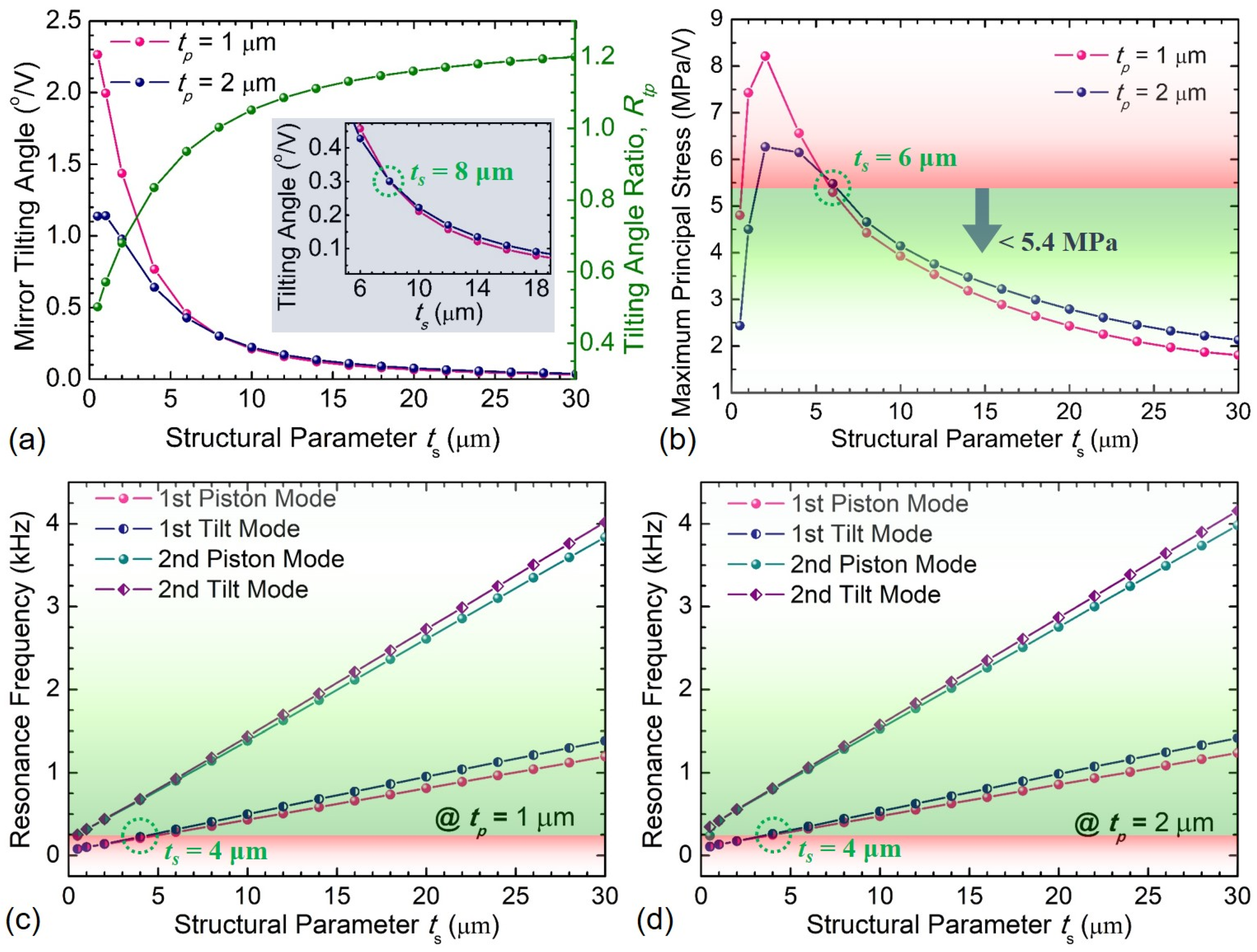
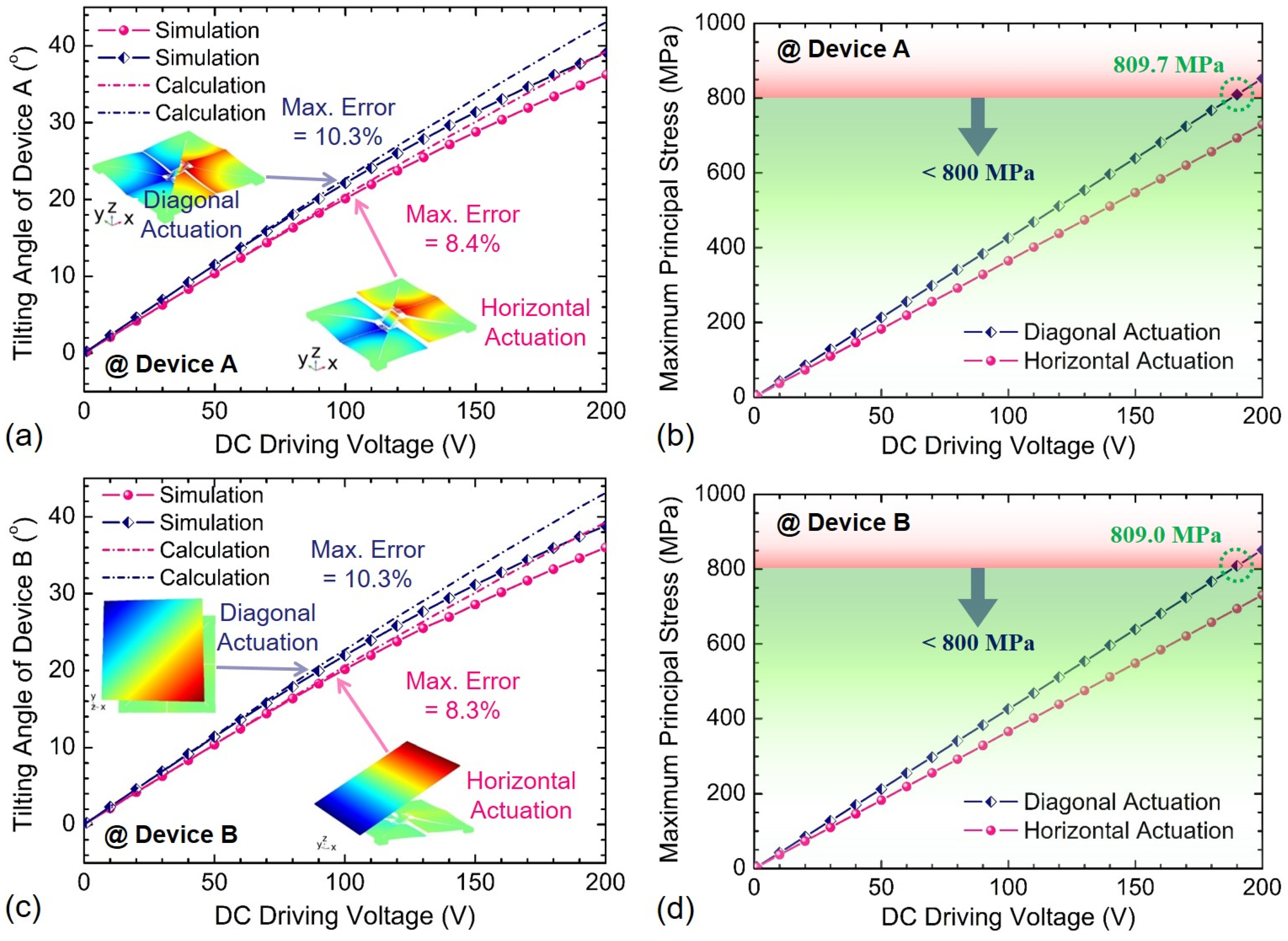
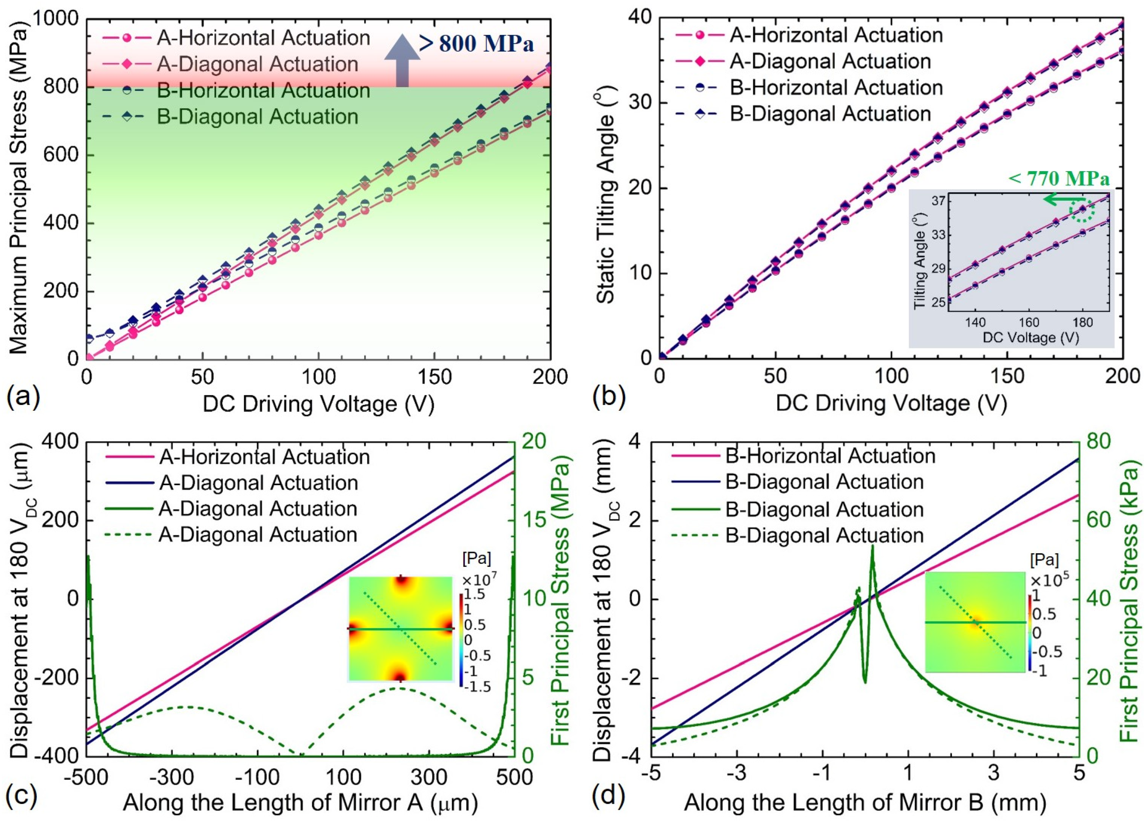
4.2. Static Actuation

After above structure optimization for Devices A and B, the optimal design parameters are determined and listed in Table 2. The static performance of both devices are firstly simulated at the static actuation modes referring to the modal shapes given in Figure 2 regardless of gravity effect, as shown in Figure 9. Both the maximum principal stress and static tilting angles almost increase linearly with the DC driving voltage changing from 0 to 200 V, with linearity of greater than 0.995. For the horizontal actuation of Device A, the tilting angle reaches up to 36.2°@200 VDC with a maximum principal stress of 729.8 MPa. As a comparison, the maximum tilting angle will be limited to 36.2°@180 VDC within the maximum principal stress of 767.2 MPa for the diagonal actuation of Device A, because the maximum principal stress of 852.4 MPa at 200 VDC will irreversibly destroy the device. The tilting angle sensitivities of Device A in horizontal and diagonal actuations are 0.1856°/VDC and 0.2011°/VDC in the DC voltage range from 0 to 180 VDC, respectively. Besides, the numerical calculations for both horizontal and diagonal tilting angles of Device A have also been made in the DC driving voltage range of 0 to 200 V, offering the theoretical tilting angle sensitivities of 0.1964°/VDC and 0.2157°/VDC, respectively. The maximum relative errors between simulations and calculations are 8.4% for horizontal actuation and 10.3% for diagonal actuation at 200 VDC. The ratios of the diagonal to horizontal maximum principal stress and von Mises stress at the same DC voltage are about 117% and 140%, respectively, which may be caused by the result of two orthogonal stresses. On the other hand, the diagonal actuation can deliver a marginally higher static tilting angle sensitivity than the horizontal actuation owing to the softer torsion springs. Moreover, the static performance of Device B is also analyzed, showing very similar characteristics to Device A. The accessible tilting angles for both horizontal and diagonal actuations of Device B are 36.0°@200 VDC and 35.9°@180 VDC, respectively. The tilting angle sensitivities of Device B in horizontal and diagonal actuations are 0.1843°/VDC and 0.1999°/VDC in the DC voltage range from 0 to 180 VDC, respectively, which are only slightly smaller than those of Device A. The explanation for the angle variation between two devices can be owing to the different mirror structures, albeit with the same piezoelectric actuators. Moreover, numerical calculations for both horizontal and diagonal tilting angles of Device B have also been undertaken in the DC driving voltage range of 0 to 200 V, offering the theoretical tilting angle sensitivities of 0.1949°/VDC and 0.2141°/VDC, respectively. The maximum relative errors between simulations and calculations for Device B were 8.3% for horizontal actuation and 10.3% for diagonal actuation at 200 VDC.
Generally, the weight impact of the millimeter-scale mirror device on its static defection performance is too small to be considered. In order to illustrate such an argument, more detailed simulations were undertaken for validation. When taking into account the gravity effect, the dependence of the material stress and tilting angle on the DC driving voltages for Devices A and B are presented in Figure 10. It is observed that both devices have excellent linearity in maximum principal stress, though in comparison Device B suffers from about 10 MPa higher stress at the same driving voltage due to the larger mirror. The static tilting angle responses of the two devices also exhibit approximately linear increase tendency in the DC voltage range from 0 to 180 VDC. The tilting angle sensitivities of Device A in horizontal and diagonal actuations are 0.1856°/VDC and 0.2010°/VDC, respectively, while those of Device B in horizontal and diagonal actuations are 0.1841°/VDC and 0.1996°/VDC, respectively. After comparing two different cases with and without consideration of the device weight, the tilting angle sensitivity variations of both devices are only within 0.2%, which is consistent with the above argument. The displacement and inner principal stress distribution along the length of both mirrors (A, B) are plotted in Figure 10c,d. The maximum principal stresses within both mirrors occur in the four spring connection points and the central region, respectively, which are much lower than the residual stress of some fabricated micromirrors [15,16,38,40]. Moreover, the displacement curves are almost perfectly linear, indicating that there are no noticeable mechanical deformations occurring during the tilting motions of both mirrors (A, B). Therefore, the gravity effect of the mirrors during the analysis can be ignored to simplify theoretical calculations and simulations. Table 4 compares the static performance of Devices A and B presented in this paper with other piezoelectric scanning mirrors reported in the literature [11,21,42,43,44]. It is demonstrated that the proposed devices tend to exhibit an outstanding θ·D product.

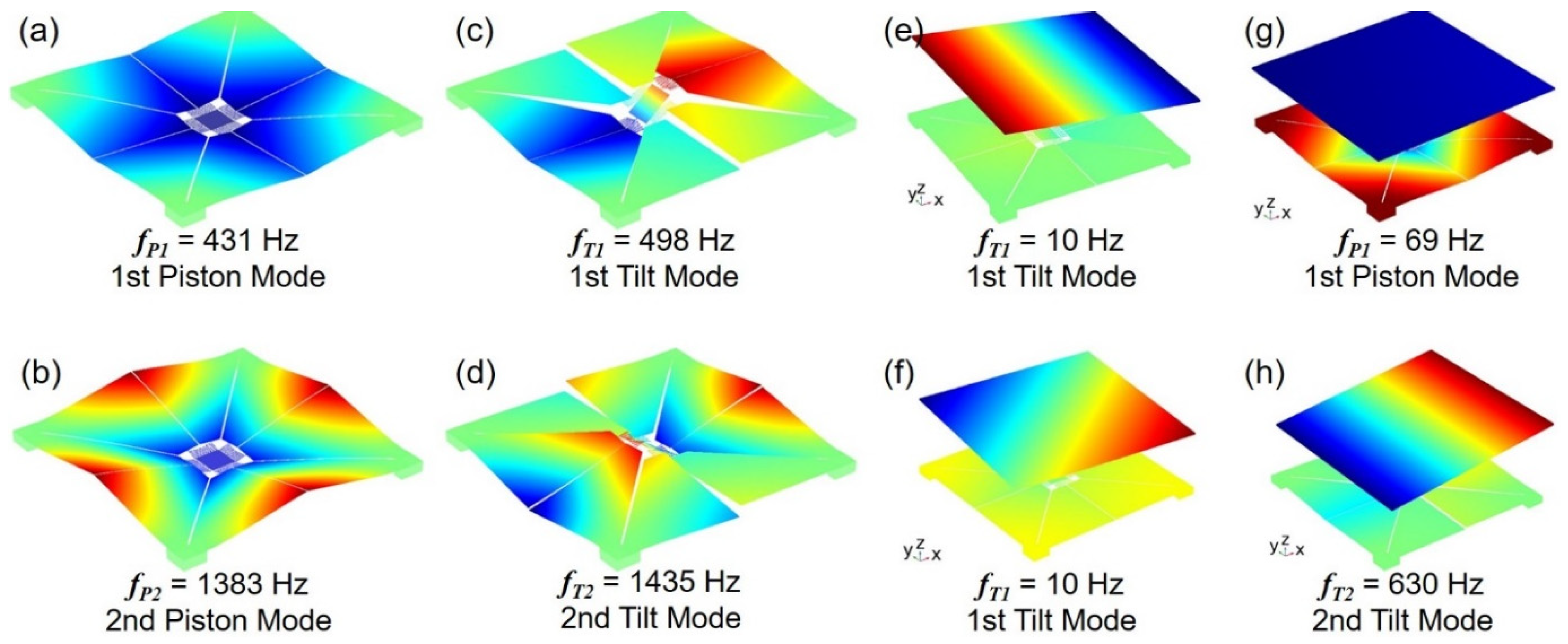
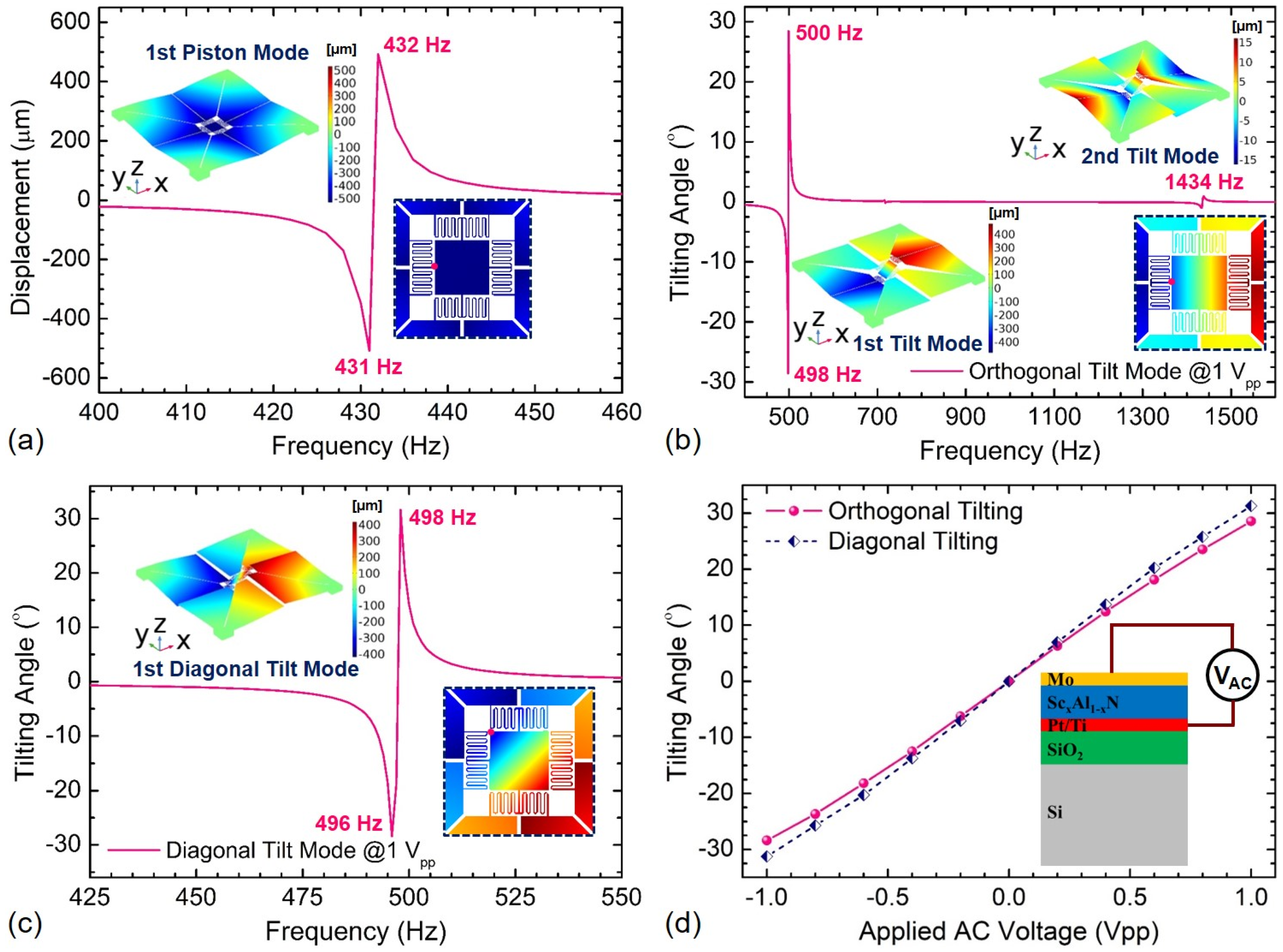
4.3. Dynamic Actuation

Both the piston and tilt vibration modes are commonly used to steer or manipulate the reflection and phase of the light. To characterize the dynamic response of the proposed MEMS scanning mirrors (Devices A and B), the modal analysis was done firstly with 3D FEM simulations, as shown in Figure 11. This shows the first-order and second-order piston mode frequencies are 431 Hz and 1383 Hz for Device A, respectively, while the first-order and second-order tilt mode frequencies are 498 Hz and 1435 Hz, respectively. The modal frequencies of larger than 400 Hz for both piston and tilt vibration modes indicates the proposed Union Jack-shaped actuators have large enough stiffness to maintain regular operation. As for Device B, the frequencies of the first-order orthogonal and diagonal tilt vibration modes have dropped to 10 Hz, while the second-order tilt mode frequency can reach to 630 Hz. Moreover, the frequency of the first-order piston vibration mode is 69 Hz. As illustrated in the mirror actuation principle (Figure 2), these different vibration modes can be excited individually or in combination with proper arrangement of the PM actuators.
All PM actuators (X1–X4, Y1–Y4) need be driven by the same alternating-current (AC) voltage if Devices A or B are expected to work at the piston vibration modes. To target the orthogonal 0°-tilt vibration modes (referring to Figure 2), the other PM actuators (X3, X4, Y3, Y4) must be excited by an opposite one when the PM actuators (X1, X2, Y1, Y2) are excited by an AC voltage applied on two electrode surfaces of the ScxAl1−xN film. On the other hand, the pair of PM actuators (X1, X4, Y1, Y4) and (X2, X3, Y2, Y3) can be configured with opposite AC voltage excitations to obtain the orthogonal 90°-tilt vibration modes. In addition, Devices A and B can also operate at the diagonal tilt modes when the pair of PM actuators (X1, X2, Y2, Y3) and (X3, X4, Y1, Y4) are excited by the opposite AC voltages. At 1 Vpp driving voltage, the simulated displacement responses at the edge of Device A are plotted in Figure 12. This shows that the proposed scanning mirror is able to work very efficiently and powerfully, offering the piston displacement sensitivity of 509 μm/Vpp at 431 Hz and the orthogonal tilt displacement sensitivities of 272 μm/Vpp at 498 Hz and 8.7 μm/Vpp at 1435 Hz. Moreover, the diagonal tilt displacement of 303 μm can be achieved by applying 1 Vpp voltage at 498 Hz, in which case the maximum principal stress in Device A is about 426 MPa. Both the orthogonal and diagonal tilting angles increases linearly with the driving voltage, offering the tilting angle sensitivities of 28.6°/Vpp and 31.3°/Vpp at 498 Hz, respectively, as shown in Figure 12d.
The dynamic response of Device B was also investigated by simulations, as shown in Figure 13. After reasonable allocation of eight PM actuators, the first-order piston displacement sensitivity is about 1542.2 μm/Vpp at 69 Hz, while the first-order orthogonal and diagonal tilting angles reach about 8.1°/Vpp and 8.9°/Vpp at 10 Hz, respectively. The maximum principal stress at the first-order tilt modes will be as high as 792.6 MPa when the applied AC voltage is 4.0 Vpp. The resonant frequencies of both the piston and tilt modes decrease dramatically because of the larger micro-mirror mass as compared to that of Device A. The products of θ·D for Devices A and B at the first-order tilt mode is about 31.3°·mm/Vpp and 88.5°·mm/Vpp, respectively, which is larger than almost all of those in the literature [4,16,21,43,44,45]. Moreover, the second-order orthogonal and diagonal tilting angles of about 0.126° was obtained when an AC voltage of 1 Vpp at 631 Hz was applied, while the maximum principal stress is at level of 160 MPa/Vpp.

5. Conclusions

In this study, a particularly efficient ScxAl1−xN-based piezoelectric MEMS scanning mirror with a pupil size of 10 mm was explored. The novel MEMS mirror, comprised a reflection mirror plate, four S-shaped meandering springs and eight trapezoidal ScxAl1−xN-based actuators, was proposed to achieve large static and dynamic two-axis tilting angles. The detailed theoretical modeling, simulations and comparative analysis for two different Sc0.41Al0.59N-based MEMS mirror designs were investigated prior to device fabrication. For the proposed Device A including a square mirror with a 1 mm length and 10 μm thickness, the maximal orthogonal and diagonal static tilting angles were ±36.2°@200 VDC and ±36.2°@180 VDC with the maximum principal stress of less than 767.2 MPa, respectively. In the dynamic actuation regime, the piston displacement sensitivity was 509 μm/Vpp at 431 Hz, and both the first-order orthogonal and diagonal tilting angles increased linearly with the driving voltage, offering the tilt angle sensitivities of 28.6°/Vpp and 31.3°/Vpp at 498 Hz, respectively. In comparison, Device B including a square mirror with a 10 mm length and 100 μm thickness was able to provide the accessible tilting angles of ±36.0°@200 VDC and ±36.9°@180 VDC for horizontal and diagonal actuations, respectively. In the dynamic actuation regime, the first-order orthogonal and diagonal tilting angles of ±8.1°/Vpp and ±8.9°/Vpp could be obtained at 10 Hz, respectively, while the second-order tilting angles are about ±0.13°/Vpp at 631 Hz. Moreover, the displacement sensitivity of Device B at the resonant piston mode was also simulated and discussed. This work has suggested from the view of FEM simulations and mathematical calculations that the right-angle trapezoidal actuators potentially possess excellent mechanical efficiency for possible optoelectronic applications thanks to the novel actuator structure design and the Union Jack-shaped arrangement.

Author Contributions

Conceptualization and methodology, C.S. and Y.L.; formal analysis, M.L., Y.L. and Y.W.; validation, C.S., Y.L. and Y.W.; investigation, C.S., B.L. and W.S.; writing—original draft preparation, C.S.; writing—review and editing, C.S., Y.L. and Y.W.; supervision, C.S. and Y.L.; project administration and funding acquisition, C.S., M.L., Y.L. and G.D. All authors have read and agreed to the published version of the manuscript.

Funding

This research was funded by the grant project of Science and Technology Research Program from Educational Committee of Hubei Province (No. Q20201309), Open Fund of Cooperative Innovation Center of Unconventional Oil and Gas (Ministry of Education and Hubei Province), Yangtze University (No. UOG2020-03), Open Fund of Key Laboratory of Exploration Technologies for Oil and Gas Resources (Yangtze University), Ministry of Education (No. K2021-18), Major Technology Innovation of Hubei Province (No.2019AAA011) and National Natural Science Foundation of China (No. 51978079).

Institutional Review Board Statement

Not applicable.

Informed Consent Statement

Not applicable.

Data Availability Statement

Data sharing not applicable.

Conflicts of Interest

The authors declare no conflict of interest. The funders had no role in the design of the study; in the collection, analyses, or interpretation of data; in the writing of the manuscript, or in the decision to publish the results.

References

  1. Holmstrom, S.T.S.; Baran, U.; Urey, H. MEMS Laser Scanners: A Review. J. Microelectromech. Syst. 2014, 23, 259–275. [Google Scholar] [CrossRef]
  2. Pollock, C.; Morrison, J.; Imboden, M.; Little, T.D.; Bishop, D.J. Beam shaping with tip-tilt varifocal mirror for indoor optical wireless communication. Opt. Express 2017, 25, 20274–20285. [Google Scholar] [CrossRef]
  3. Sato, K.; Okutsu, K. Basic Characteristics of a Micromechanical Optical Switch Using an S-Shaped Deformable Thin-Film Mirror. J. Lightwave Technol. 2011, 29, 2805–2811. [Google Scholar] [CrossRef]
  4. Baran, U.; Brown, D.; Holmstrom, S.; Balma, D.; Davis, W.O.; Muralt, P.; Urey, H. Resonant PZT MEMS Scanner for High-Resolution Displays. J. Microelectromech. Syst. 2012, 21, 1303–1310. [Google Scholar] [CrossRef] [Green Version]
  5. Lin, L.Y.; Keeler, E.G. Progress of MEMS Scanning Micromirrors for Optical Bio-Imaging. Micromachines 2015, 6, 1675–1689. [Google Scholar] [CrossRef] [Green Version]
  6. Wolter, A.; Hsu, S.-T.; Schenk, H.; Lakner, H.K. Applications and requirements for MEMS scanner mirrors. In Proceedings of the SPIE 5719, MOEMS and Miniaturized Systems V, San Jose, CA, USA, 25–26 January 2005; pp. 64–75. [Google Scholar]
  7. Wu, L.; Xie, H. Large-aperture, rapid scanning MEMS micromirrors for free-space optical communications. In Proceedings of the IEEE/LEOS International Conference on Optical MEMS and Nanophotonics 2009, Clearwater, FL, USA, 17–20 August 2009; pp. 131–132. [Google Scholar]
  8. Ye, L.; Zhang, G.; You, Z. Large-Aperture kHz Operating Frequency Ti-alloy Based Optical Micro Scanning Mirror for LiDAR Application. Micromachines 2017, 8, 120. [Google Scholar] [CrossRef]
  9. Liu, Y.; Xu, J.; Zhong, S.; Wu, Y. Large size MEMS scanning mirror with vertical com drive for tunable optical filter. Opt. Laser. Eng. 2013, 51, 54–60. [Google Scholar] [CrossRef]
  10. Jung, I.W.; Krishnamoorthy, U.; Solgaard, O. High Fill-Factor Two-Axis Gimbaled Tip-Tilt-Piston Micromirror Array Actuated by Self-Aligned Vertical Electrostatic Combdrives. J. Microelectromech. Syst. 2006, 15, 563–571. [Google Scholar] [CrossRef]
  11. Gu-Stoppel, S.; Lisce, T.; Fichtner, S.; Funck, N.; Claus, M.; Wagner, B.; Lofink, F. AlScN based MEMS quasi-static mirror matrix with large tilting angle and high linearity. Sens. Actuators A Phys. 2020, 312, 112107. [Google Scholar] [CrossRef]
  12. Zhang, W.; Li, P.; Zhang, X.; Wang, Y.; Hu, F. InGaN/GaN micro mirror with electrostatic comb drive actuation integrated on a patterned silicon-on-insulator wafer. Opt. Express 2018, 26, 7672–7682. [Google Scholar] [CrossRef]
  13. Alneamy, A.; Khater, M.; Al-Ghamdi, M.; Park, S.; Heppler, G.; Abdel-Rahman, E.M. Dual Actuation Micro-mirrors. J. Micromech. Microeng. 2018, 28, 075014. [Google Scholar] [CrossRef]
  14. Tan, J.; Sun, W.; Yeow, J. Internal Model-Based Robust Tracking Control Design for the MEMS Electromagnetic Micromirror. Sensors 2017, 17, 1215. [Google Scholar] [CrossRef] [Green Version]
  15. Tanguy, Q.A.A.; Bargiel, S.; Xie, H.; Passilly, N.; Barthès, M.; Gaiffe, O.; Rutkowski, J.; Lutz, P.; Gorecki, C. Design and Fabrication of a 2-Axis Electrothermal MEMS Micro-Scanner for Optical Coherence Tomography. Micromachines 2017, 8, 146. [Google Scholar] [CrossRef]
  16. Chen, S.-H.; Michael, A.; Kwok, C.Y. Design and Modeling of Piezoelectrically Driven Micro-Actuator with Large Out-of-Plane and Low Driving Voltage for Micro-Optics. J. Microelectromech. Syst. 2019, 28, 919–932. [Google Scholar] [CrossRef]
  17. Tsai, J.; Lu, L.; Hsu, W.; Sun, C.; Wu, M.C. Linearization of a two-axis MEMS scanner driven by vertical comb-drive actuators. J. Micromech. Microeng. 2008, 18, 015015. [Google Scholar] [CrossRef] [Green Version]
  18. Cheng, J.; Liu, W.; Chen, Q.; Xu, N.; Sun, Q.; Liu, Y.; Xie, H. A mems variable optical attenuator based on a vertical comb drive with self-elevated stators. Sens. Actuators A Phys. 2017, 271, 398–408. [Google Scholar] [CrossRef]
  19. Song, Y.; Panas, R.M.; Hopkins, J.B. A review of micromirror arrays. Precis. Eng. 2017, 51, 729–761. [Google Scholar] [CrossRef]
  20. Li, G.; Zuo, P.; Xie, W.; Yeow, J.T.W. Dynamic modeling of a polymer composite based hard-magnetic micro-mirror. In Proceedings of the 34th Chinese Control Conference (CCC), Hangzhou, China, 28–30 July 2015; pp. 8362–8367. [Google Scholar]
  21. Shao, J.; Li, Q.; Feng, C.; Li, W.; Yu, H. AlN based piezoelectric micromirror. Opt. Lett. 2018, 43, 987–990. [Google Scholar] [CrossRef] [PubMed]
  22. Meinel, K.; Stoeckel, C.; Melzer, M.; Zimmermann, S.; Forke, R.; Hiller, K.; Otto, T. Piezoelectric scanning micromirror with built-in sensors based on thin film aluminum nitride. IEEE Sens. J. 2020, 21, 9682–9689. [Google Scholar] [CrossRef]
  23. Meinel, K.; Melzer, M.; Stoeckel, C.; Shaporin, A.; Forke, R.; Zimmermann, S.; Hiller, K.; Otto, T.; Kuhn, H. 2D Scanning Micromirror with Large Scan Angle and Monolithically Integrated Angle Sensors Based on Piezoelectric Thin Film Aluminum Nitride. Sensors 2020, 20, 6599. [Google Scholar] [CrossRef] [PubMed]
  24. Mohith, S.; Upadhya, A.R.; Navin, K.P.; Kulkarni, S.M.; Rao, M. Recent trends in piezoelectric actuators for precision motion and their applications: A review. Smart Mater. Struct. 2021, 30, 013002. [Google Scholar] [CrossRef]
  25. Lei, H.; Wen, Q.; Yu, F.; Li, D.; Shang, Z.; Huang, J.; Wen, Z. AlN film based piezoelectric large-aperture MEMS scanning micromirror integrated with angle sensors. J. Micromech. Microeng. 2018, 28, 115012. [Google Scholar] [CrossRef]
  26. Mayrhofer, P.M.; Rehlendt, C.; Fischeneder, M.; Kucera, M.; Wistrela, E.; Bittner, A.; Schmid, U. ScAlN MEMS Cantilevers for Vibrational Energy Harvesting Purposes. J. Microelectromech. Syst. 2017, 26, 102–112. [Google Scholar] [CrossRef]
  27. Caro, M.A.; Zhang, S.; Riekkinen, T.; Ylilammi, M.; Moram, M.A.; Lopez-Acevedo, O.; Molarius, J.; Laurila, T. Piezoelectric coefficients and spontaneous polarization of ScAlN. J. Phys. Condens. Matter 2015, 27, 279602. [Google Scholar] [CrossRef]
  28. Gu-Stoppel, S.; Lisec, T.; Claus, M.; Funck, N.; Fichtner, S.; Schröder, S.; Wagner, B.; Lofink, F. A triple-wafer-bonded AlScN driven quasi-static MEMS mirror with high linearity and large tilt angles. In Proceedings of the SPIE MOEMS and Miniaturized Systems XIX, San Francisco, CA, USA, 28 February 2020; p. 1129304. [Google Scholar]
  29. Gu-Stoppel, S.; Lisec, T.; Fichtner, S.; Funck, N.; Eisermann, C.; Lofink, F.; Wagner, B.; Müller-Groeling, A. A highly linear piezoelectric quasi-static MEMS mirror with mechanical tilt angles of larger than 10°. In Proceedings of the SPIE MOEMS and Miniaturized Systems XVIII, San Francisco, CA, USA, 4 March 2019; p. 1093102. [Google Scholar]
  30. Sun, C.; Li, B.; Su, W.; Liu, Y.; Wu, Y. Modeling and Optimization of ScAlN-based MEMS Mirror with Large Static Two-axis Tilting Angle. In Proceedings of the 16th International Conference on Nano/Micro Engineered and Molecular Systems (NEMS), Xiamen, China, 25–29 April 2021; pp. 704–708. [Google Scholar]
  31. Li, F.; Zhou, P.; Wang, T.; He, J.; Yu, H.; Shen, W. A Large-Size MEMS Scanning Mirror for Speckle Reduction Application. Micromachines 2017, 8, 140. [Google Scholar] [CrossRef] [Green Version]
  32. Akiyama, M.; Umeda, K.; Honda, A.; Nagase, T. Influence of scandium concentration on power generation figure of merit of scandium aluminum nitride thin films. Appl. Phys. Lett. 2013, 102, 021915. [Google Scholar] [CrossRef]
  33. Barth, S.; Bartzsch, H.; Gloess, D.; Frach, P.; Herzog, T.; Walter, S.; Heuer, H. Sputter deposition of stress-controlled piezoelectric AlN and ScAlN films for ultrasonic and energy harvesting applications. IEEE Trans. Ultrason. Ferroelectr. Freq. Control 2014, 61, 1329–1334. [Google Scholar] [CrossRef] [PubMed]
  34. Ballas, R.G. Piezoelectric Multilayer Beam Bending Actuators: Static and Dynamic Behavior and Aspects of Sensor Integration; Springer: Berlin, Germany, 2007; pp. 47–121. [Google Scholar]
  35. Timoshenko, S.P.; Weaver, W.; Young, D.H. Vibration Problems in Engineering, 5th ed.; John Wiley & Sons: New York, NY, USA, 1990; pp. 1–107. [Google Scholar]
  36. Akiyama, M.; Kano, K.; Teshigahara, A. Influence of growth temperature and scandium concentration on piezoelectric response of scandium aluminum nitride alloy thin films. Appl. Phys. Lett. 2009, 95, 162107. [Google Scholar] [CrossRef]
  37. Fichtner, S.; Wolff, N.; Krishnamurthy, G.; Petraru, A.; Bohse, S.; Lofink, F.; Chemnitz, S.; Kohlstedt, H.; Kienle, L.; Wagner, B. Identifying and overcoming the interface originating c-axis instability in highly Sc enhanced AlN for piezoelectric micro-electromechanical systems. J. Appl. Phys. 2017, 122, 035301. [Google Scholar] [CrossRef]
  38. Mertin, S.; Heinz, B.; Rattunde, O.; Christmann, G.; Dubois, M.-A.; Nicolay, S.; Muralt, P. Piezoelectric and structural properties of c-axis textured aluminium scandium nitride thin films up to high scandium content. Surf. Coat. Tech. 2018, 343, 2–6. [Google Scholar] [CrossRef]
  39. Wang, H.; Lv, Y.; Wang, C.; Wang, X.; He, C.; Xue, C.; He, S. Simulation Analysis and Performance Testing Investigation of Capacitive Micromachined Ultrasonic Transducer. Int. J. Pattern Recogn. 2018, 32, 1858004. [Google Scholar] [CrossRef]
  40. Michael, A.; Kwok, C.Y. Piezoelectric micro-lens actuator. Sens. Actuators A Phys. 2015, 236, 116–129. [Google Scholar] [CrossRef]
  41. Akiyama, M.; Kamohara, T.; Kano, K.; Teshigahara, A.; Takeuchi, Y.; Kawahara, N. Enhancement of piezoelectric response in scandium aluminum nitride alloy thin films prepared by dual reactive cosputtering. Adv. Mater. 2009, 21, 593–596. [Google Scholar] [CrossRef] [PubMed]
  42. Jing, Z.; Xu, M.; Feng, B. Modeling and optimization of a novel two-axis mirror-scanning mechanism driven by piezoelectric actuators. Smart Mater. Struct. 2015, 24, 025002. [Google Scholar] [CrossRef]
  43. Koh, K.H.; Kobayashi, T.; Lee, C. Investigation of piezoelectric driven MEMS mirrors based on single and double S-shaped PZT actuator for 2-D scanning applications. Sens. Actuators A Phys. 2012, 184, 149–159. [Google Scholar] [CrossRef]
  44. Lee, C.; Hsiao, F.-L.; Kobayashi, T.; Koh, K.H.; Ramana, P.V.; Xiang, W.; Yang, B.; Tan, C.W.; Pinjala, D. A 1-V Operated MEMS Variable Optical Attenuator Using Piezoelectric PZT Thin-Film Actuators. IEEE J. Sel. Top. Quant. 2009, 15, 1529–1536. [Google Scholar]
  45. Ye, L.; Zhang, G.; You, Z. 5 V Compatible Two-Axis PZT Driven MEMS Scanning Mirror with Mechanical Leverage Structure for Miniature LiDAR Application. Sensors 2017, 17, 521. [Google Scholar] [CrossRef] [Green Version]
Figure 1. Architectures of two ScxAl1−xN-based micro-electro-mechanical systems (MEMS) mirrors: (a) Device A, (b) Device B, (c) Union Jack-shaped actuators and S-shaped meandering springs.
Sensors 21 05513 g001
Figure 2. Mirror actuation principle for (ad) 0°, 45°, 90° and 135°tilting angles when only using four PM actuators; (eh) 0°, 45°, 90° and 135° tilting angles when using eight PM actuators.
Sensors 21 05513 g002
Figure 3. Simplified structural model of the trapezoidal ScxAl1−xN based actuators: (a) structure configuration of the MEMS mirror, (b) top view of the PM actuator, (c) design schematic of the meandering spring, (d) cross-sectional view of the PM actuator, (e) simplification of the MEMS mirror.
Sensors 21 05513 g003
Figure 4. Meshing of the entire geometry of the proposed device.
Sensors 21 05513 g004
Figure 5. FEM simulations of material principal stress and defection in three piezoelectric MEMS mirrors with different meandering spring designs at 1 VDC driving voltage: (a) rectangular-shaped spring, (b,c) S-shaped springs.
Sensors 21 05513 g005
Figure 6. The dependence of the static tilting angles on the structural parameters: (a) θ0, (b) l1, (c) w0 and (d) w2.
Sensors 21 05513 g006
Figure 7. Simulation results of the MEMS scanning mirrors varying with the thickness ts of the Si device layer: (a) mirror tilting angle, (b) maximum principal stress, (c,d) resonance frequencies of different modes.
Sensors 21 05513 g007
Figure 8. Dependence of the mechanical tilting angle and maximum principal stress on the Sc content: (a) mirror tilting angle, (b) angle-stress ratio.
Sensors 21 05513 g008
Figure 9. Comparison of dependence of the tilting angle and maximum principal stress on the DC driving voltages: (a,b) Device A without gravity, (c,d) Device B without gravity.
Sensors 21 05513 g009
Figure 10. Comparison of dependence of the maximum principal stress and tilting angle on the DC driving voltages for Devices A and B with gravity: (a) maximum principal stress, (b) static tilting angle, (c,d) displacement.
Sensors 21 05513 g010
Figure 11. Simulated piston and tilt vibration modes: (ad) Device A; (eh) Device B.
Sensors 21 05513 g011
Figure 12. Frequency response of Device A: (a) displacement at the piston mode, (b) tilting angle at the 1st and 2nd orthogonal tilt modes, (c) tilting angle at the diagonal tilt mode, (d) tilting angle vs. applied AC voltage.
Sensors 21 05513 g012
Figure 13. Frequency response of Device B: (a,b) displacement at the 1st and 2nd tilt modes, (c,d) tilting angle vs. applied AC voltage.
Sensors 21 05513 g013
Table 1. Comparison between ScAlN, AlN and PbZrxTi1−xO3 (PZT) piezoelectric materials.
PerformanceSc0.41Al0.59N [11,27,32]AlN [11,26]PZT [11,26]
Material CategoryNon-ferroelectricFerroelectric
Piezoelectric Coefficient, e 31 , f [C/m2]~3.16~1.1~21
Relative Permittivity, ε r 16.7101300
Figure of Merit (FoM), e 31 , f 2 / ε 0 ε r [GPa]67.513.738.3
Highest DC Driving Voltage [V]±200±200±30
DirectionalityBidirectionalUnidirectional
CMOS compatibilityYesNo
Table 2. Geometrical parameter specifications of mirror devices A and B.
ParameterDevice ADevice B
Mirror length, lA or lB [μm]100010,000
Thickness of the mirror plate, tA or tB [μm]10100
Length of the pillar, lp [μm]-250
Height of the pillar, hp [μm]-3500
Length of the PM actuator, l1 [μm]4025
Fixed boundary width of the PM actuator, w0 [μm]700
Lower width of the PM actuator, w1 [μm]3035
Upper width of the PM actuator, w2 [μm]880
Length of the meandering spring, lm [μm]370
Width of the meandering spring, wm [μm]20
Spacing pitch of the meandering spring, wp [μm]120
Length of the torsion bar, lb [μm]390
Width of the torsion bar, wb [μm]20
Length of the connecting bar, lc [μm]410
Width of the connecting bar, wc [μm]20
Table 3. Material properties used in the simulation of both devices A and B [4,8,16,23,39,40].
ParameterSiSiO2PtMoAu
Young’s Modulus [GPa]1707016831270
Poisson’s Ratio0.280.170.380.310.44
Density [kg/m3]2329220021,45010,20019,300
Relative Permittivity11.74.2---
Table 4. Static performance comparison between the MEMS mirrors presented here and in the literature.
Piezoelectric MirrorsMaterialMirror Size, D [mm]Tilt Angle, θ [°/V]Maximum Angle, θmax [°]θ·D [°·mm/V]
Device AScAlN10.2011±36.2 @180 V0.201
Device BScAlN100.1999±36.0 @180 V1.999
Ref. [11]ScAlN0.80.0933±14.00 @150 V0.075
Ref. [21]AlN0.20.005±0.15 @30 V0.001
Ref. [42]Bulk PZT200.02243.14 @120 V0.449
Ref. [43]PZT20.464.60 @10 V0.920
Ref. [44]PZT20.35.10 @17 V0.600
Publisher’s Note: MDPI stays neutral with regard to jurisdictional claims in published maps and institutional affiliations.

