A MEMS Ultra-Wideband (UWB) Power Sensor with a Fe-Co-B Core Planar Inductor and a Vibrating Diaphragm Capacitor
Abstract
1. Introduction
2. Principle of Operation
3. Theoretical Modeling
4. Sensor Design and Simulation
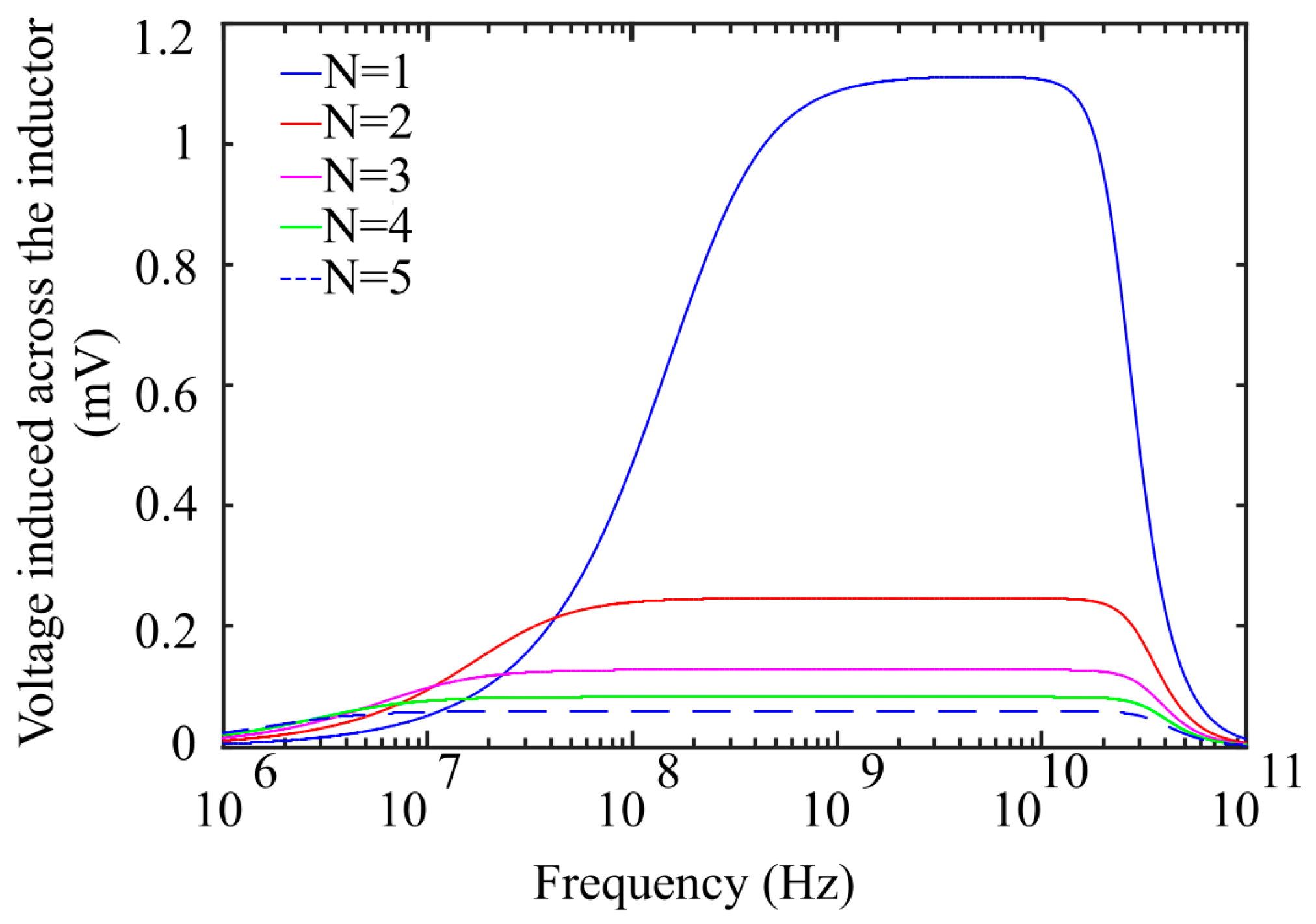
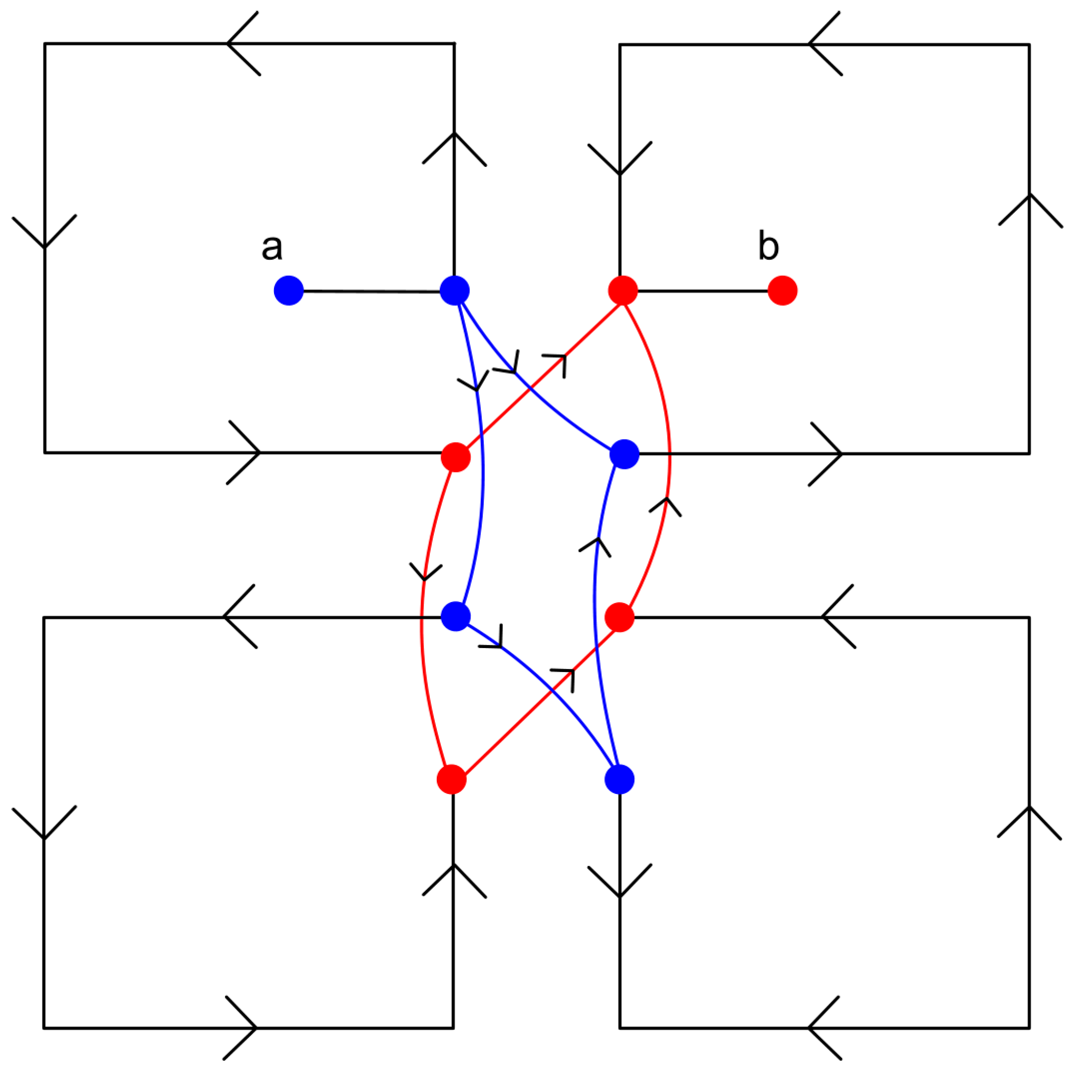
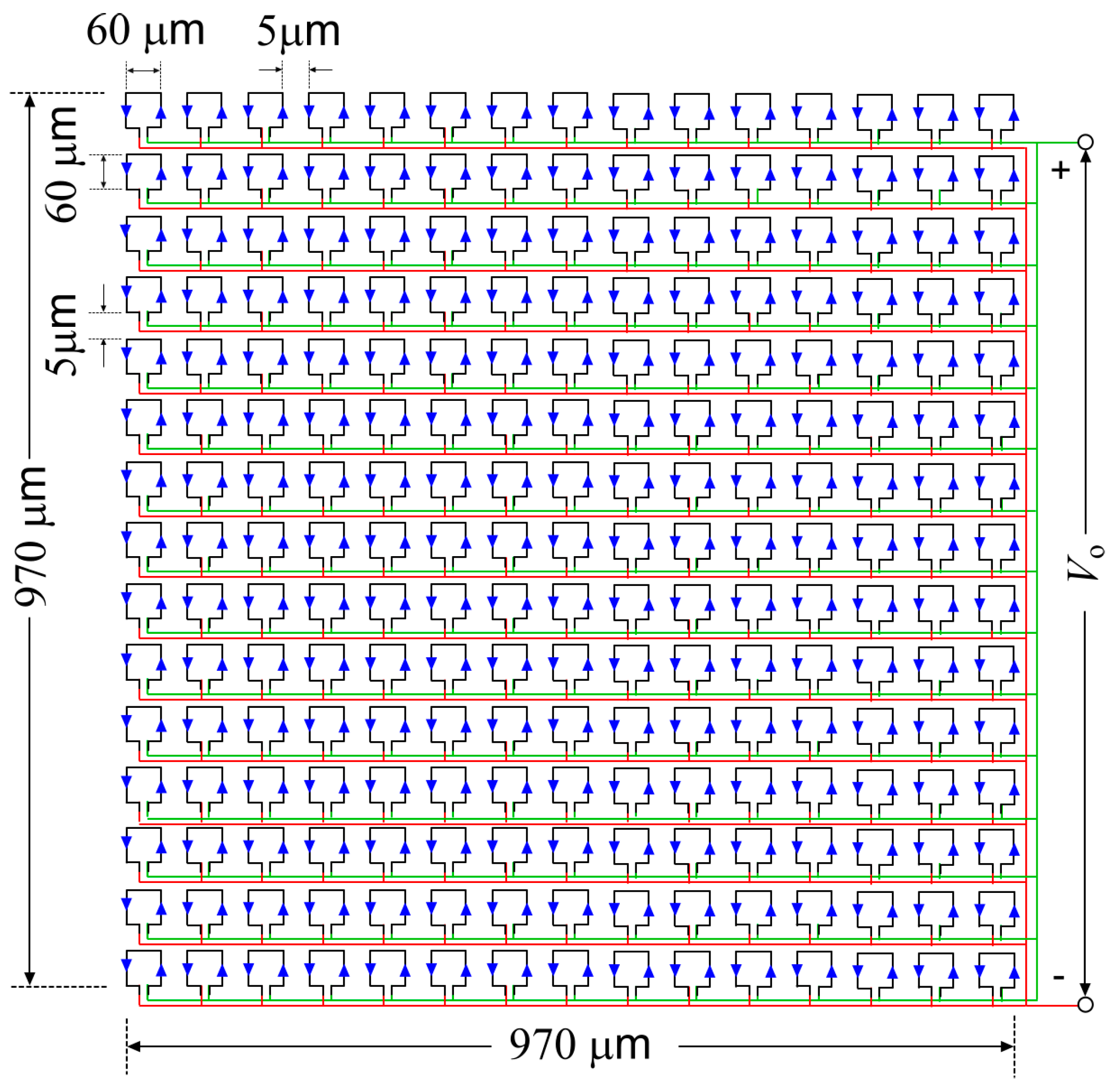
4.1. Flat Frequency Response for the Antenna Loop
4.2. MEMS Capacitor Design
4.3. Material Selection
5. Results
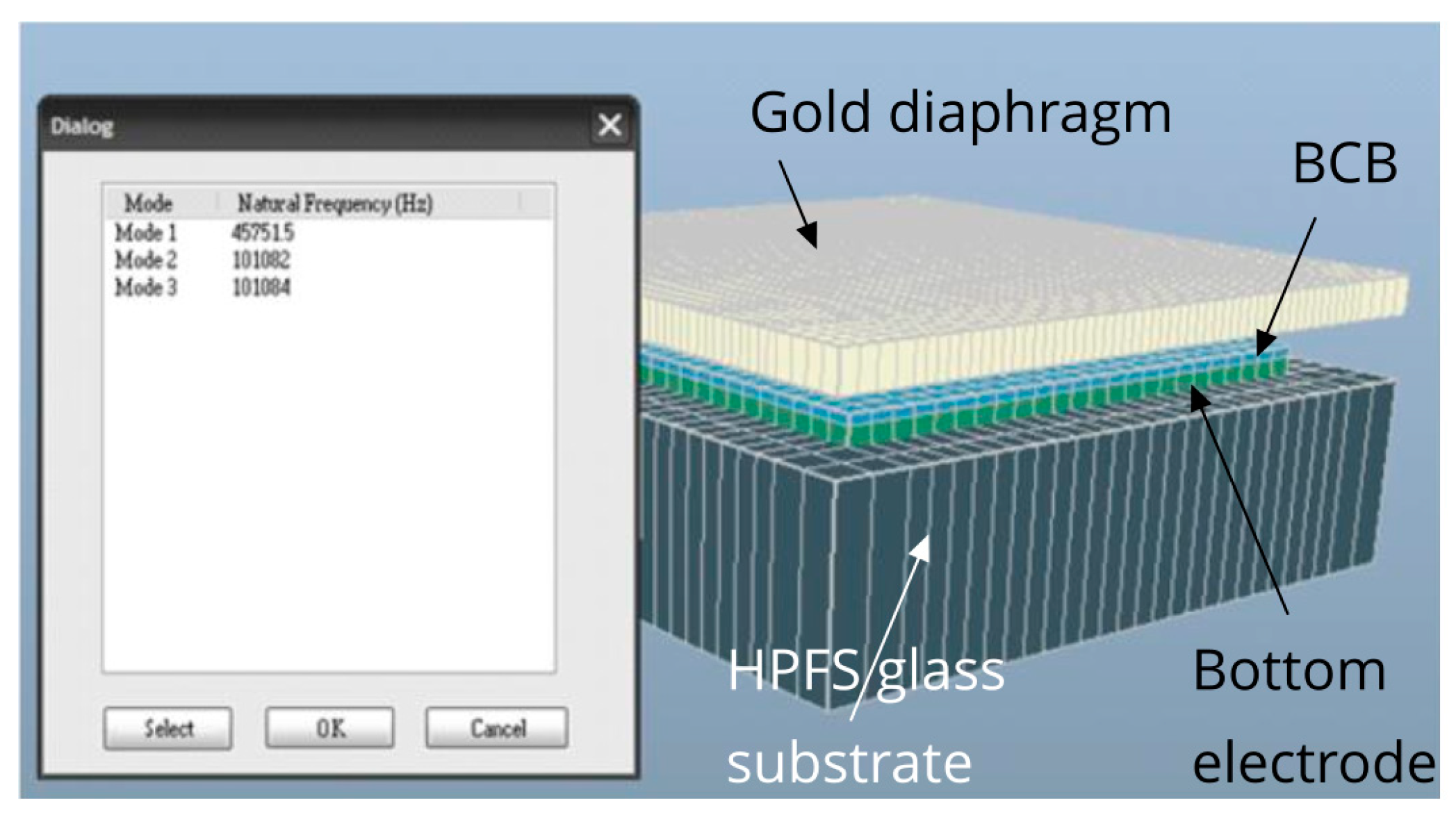
5.1. Resonant Frequency Simulation
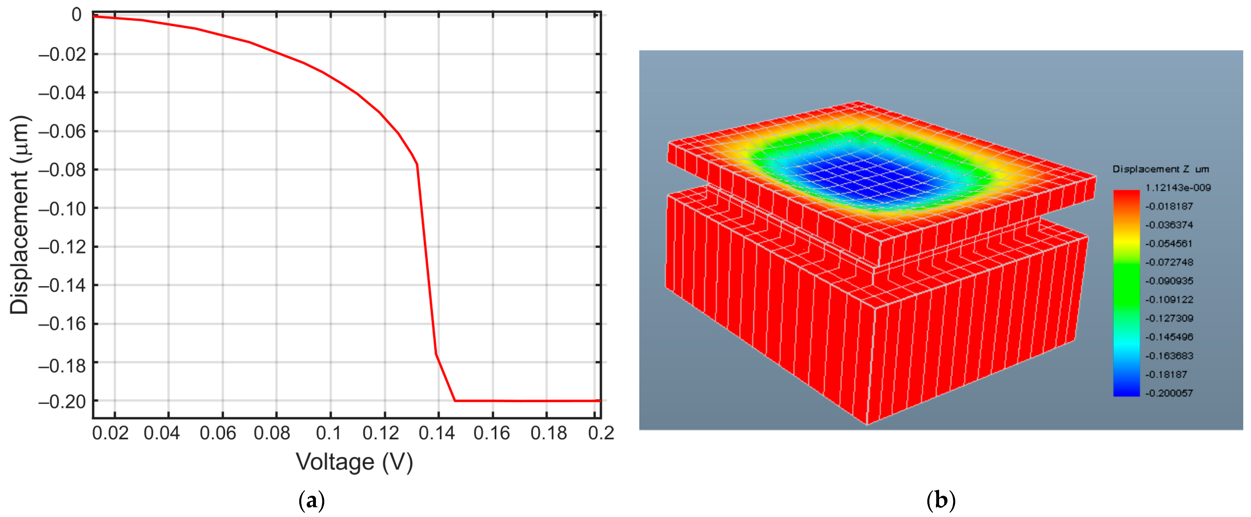
5.2. Electromechanical 3D FEA Simulation of Pull-in Voltage of the MEMS Capacitor
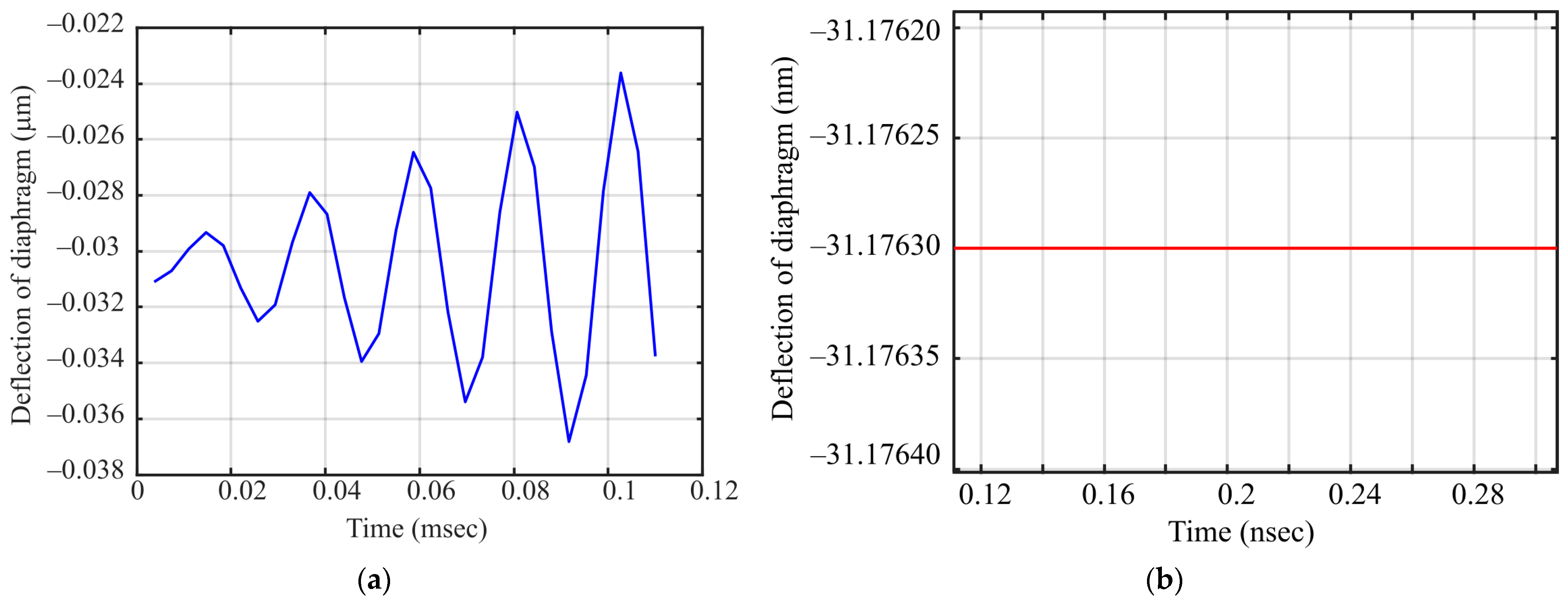
5.3. Dynamic Analysis
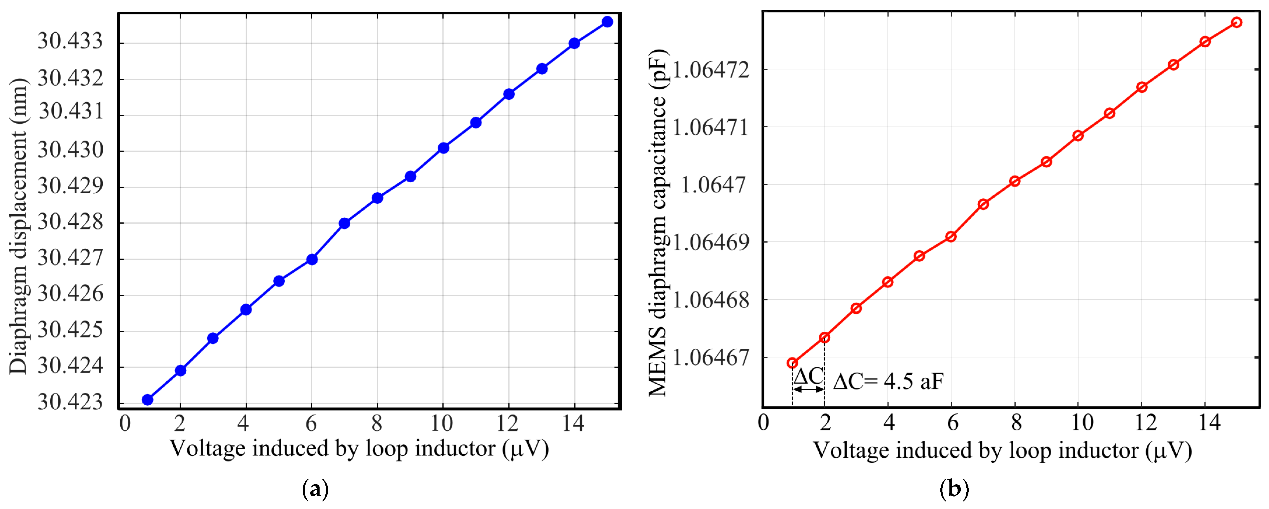
5.4. Sensitivity Calculation
6. Discussion
7. Conclusions
Author Contributions
Funding
Institutional Review Board Statement
Informed Consent Statement
Data Availability Statement
Acknowledgments
Conflicts of Interest
References
- Federal Communications Commission. Revision of Part 15 of the Commission’s Rules Regarding Ultra-Wideband Transmission Systems; First Report and Order, FCC 02-48; Federal Communications Commission: Washington, DC, USA, 2002. Available online: https://www.fcc.gov/document/revision-part-15-commissions-rules-regarding-ultra-wideband-7 (accessed on 15 March 2021).
- Taylor, J. Ultrawideband Radar Future Directions and Benefits. In Proceedings of the Progress in Electromagnetics Research Symposium, Stockholm, Sweden, 12–15 August 2013; pp. 1575–1578. [Google Scholar]
- Jofre, L.; Broquetas, A.; Romeu, J.; Blanch, S.; Toda, A.; Fabregas, X.; Cardama, A. UWB Tomographic Radar Imaging of Penetrable and impenetrable objects. Proc. IEEE 2009, 97, 451–464. [Google Scholar] [CrossRef]
- Vorst, A.; Rosen, A.; Kotsuka, Y. RF/Microwave Interaction with Biological Tissues; Wiley-IEEE Press: Hoboken, NJ, USA, 2006; pp. 63–91. [Google Scholar]
- Murphy, Q. Radar Tomography: A New Concept in Medical Imaging. Ann. Dent. 1994, 53, 5–14. [Google Scholar]
- Paulson, C.; Chang, J.; Romero, C.; Watson, J.; Pearce, F.; Levin, N. Ultra-wideband Radar Methods and Techniques of Medical Sensing and Imaging. In Smart Medical and Biomedical Sensor Technology III, Proceedings of the SPIE—The International Society for Optical Engineering 6007 Boston, MA, USA, 11 November 2005; SPIE: Bellingham, WA, USA, 2005; pp. 96–107. [Google Scholar]
- Townsend, K.; Haslett, J. A Wideband Power Detection System Optimized for the UWB Spectrum. IEEE J. Solid-State Circuits 2009, 44, 371–381. [Google Scholar] [CrossRef]
- Yin, Q.; Eisenstadt, W.; Fox, R.; Zhang, T. A translinear RMS detector for embedded test of RF ICs. IEEE Trans. Instrum. Meas. 2005, 15, 1708–1714. [Google Scholar] [CrossRef]
- Lorona, A.; Messer, I.; Forsyth, S. RF Power Measurement Basics; Agilent Technologies: Santa Clara, CA, USA, 2001; pp. 1–27. [Google Scholar]
- Sakphrom, S.; Thanachayanont, A. A Low-Power CMOS RF Power Detector. In Proceedings of the 19th IEEE International Conference on Electronics, Circuits, and Systems (ICECS 2012), Seville, Spain, 9–12 December 2012; pp. 177–180. [Google Scholar]
- Fernandez, L.; Wiegerink, R.; Flokstra, J.; Ses´e, J.; Jansen, H.; Elwenspoek, M. A capacitive RF power sensor based on MEMS technology. J. Micromech. Microeng. 2006, 1, 1099–1107. [Google Scholar] [CrossRef]
- Ferrari, G.; Fumagalli, L.; Sampietro, M.; Prati, E. CMOS Fully Compatible Microwave Detector Based on MOSFET Operating in Resistive Regime. IEEE Microw. Wirel. Compon. Lett. 2005, 15, 445–447. [Google Scholar] [CrossRef]
- Shafah, E.; Moulay, A.; Djerafi, T. A 2.45 GHz Signal Detector Based on Zero Biasing Field Effect Transistor. In Proceedings of the 2019 49th European Microwave Conference (EuMC), Paris, France, 1–3 October 2019; pp. 1–4. [Google Scholar]
- Zhou, Y.; Chia, M. A Low-Power Ultra-Wideband CMOS True RMS Power Detector. IEEE Trans. Microw. Theory Tech. 2008, 56, 1052–1058. [Google Scholar] [CrossRef]
- Li, C.; Gong, F.; Wang, P. A Low-Power Ultrawideband CMOS Power Detector with an Embedded Amplifier. IEEE Trans. Instrum. Meas. 2010, 59, 3270–3278. [Google Scholar] [CrossRef]
- Valdes-Garcia, A.; Venkatasubramanian, R.; Silva-Martinez, J.; Sánchez-Sinencio, E. A Broadband CMOS Amplitude Detector for On-Chip RF Measurements. IEEE Trans. Instrum. Meas. 2008, 57, 1470–1477. [Google Scholar] [CrossRef]
- Gao, Y.; Xu, W.; Kong, C.; Tang, Z. A Broadband Power Detector with Temperature and Process compensation. In Proceedings of the 2017 IEEE 12th International Conference on ASIC (ASICON), Guiyang, China, 25–28 October 2017; pp. 722–725. [Google Scholar]
- Qayyum, S.; Negra, R. 0.8 mW, 0.1–110 GHz RF Power Detector with 6 GHz Video Bandwidth for Multigigabit Software Defined Radios. In Proceedings of the 2017 IEEE MTT-S International Microwave Symposium (IMS), Honololu, HI, USA, 4–9 June 2017; pp. 1722–1725. [Google Scholar]
- Moulay, A.; Djerafi, T. Multi-Stage Schottky Diode Power Harvester for UWB application. In Proceedings of the 2018 IEEE Wireless Power Transfer Conference (WPTC), Montreal, QC, Canada, 3–7 June 2018; pp. 1–4. [Google Scholar]
- Pirouz, A. Capacitive Micromachined Ultrasound Transducer (CMUT) Design and Fabrication for Intracardiac Echocardiography. Ph.D. Thesis, Georgia Institute of Technology, Atlanta, GA, USA, 2019. [Google Scholar]
- Wright, A.; Wu, W.; Oppenheim, I.; Greve, D. Damping, Noise, and In-Plane Response of MEMS Acoustic Emission Sensors. J. Acoust. Emiss. 2007, 25, 115–123. [Google Scholar]
- Corning, Inc. Semiconductor Glass Products. Available online: https://docplayer.net/45096334-Semiconductor-glass-products-corning-semiconductor-glass-wafers.html (accessed on 2 December 2020).
- Nieminen, H.; Ermolov, V.; Nybergh, K.; Silanto, S.; Ryhänen, T. Microelectromechanical capacitors for RF applications. J. Micromech. Microeng. 2002, 12, 177–186. [Google Scholar] [CrossRef]
- Kosatsky, T. Radiofrequency Toolkit for Environmental Health Practitioners; British Columbia Centre for Disease Control (BCCDC): Vancouver, BC, USA, 2013; pp. 13–25.
- Vejella, S. A MEMS-based Microwave Pixel for UWB Radar Based 3-D Diagnostic Imaging. Master’s Thesis, University of Windsor, Windsor, ON, USA, 2017. [Google Scholar]
- Stutzman, W.; Thiele, G. Antenna Theory and Design, 3rd ed.; John Wiley & Sons, Inc.: Hoboken, NJ, USA, 2013; pp. 81–89. [Google Scholar]
- Feng, Y.; Benjamin, B.; Nelson, R. Analytical Expressions for Small Loop Antennas—With Applicaton to EMC and RFID Systems. In Proceedings of the IEEE International Symposium on Electromagnetic Compatibility, Portland, OR, USA, 14–18 August 2006; pp. 1–6. [Google Scholar]
- Lionet, L. Magnetic Loop Antenna Theory. Available online: https://sidstation.loudet.org/antenna-theory-en.xhtml (accessed on 10 November 2020).
- Maadi, M.; Zemp, R. A Nonlinear Lumped Equivalent Circuit Model for a Single Uncollapsed Square CMUT Cell IEEE Transactions on Ultrasonics. IEEE Trans. Ultrason. Ferroelectr. Freq. Control 2019, 66, 1340–1351. [Google Scholar] [CrossRef] [PubMed]
- Oguz, H.; Olcum, S.; Senlik, M.; Tas, V.; Atalar, A.; Koymen, H. Nonlinear Modeling of an Immersed Transmitting Capacitive Micromachined Ultrasonic Transducer for Harmonic Balance Analysis. IEEE Trans. Ultrason. Ferroelectr. Freq. Control 2010, 57, 438–447. [Google Scholar] [CrossRef] [PubMed]
- Wygant, I.; Kupnik, M.; Khuri-Yakub, B. Analytically Calculating Membrane Displacement and the Equivalent Circuit Model of a Circular CMUT Cell. In Proceedings of the 2008 IEEE International Ultrasonics Symposium, Beijing, China, 2–5 November 2008; pp. 2111–2114. [Google Scholar]
- Rahman, M.; Hernandez, J.; Chowdhury, S. An Improved Analytical Method to Design CMUTs With Square Diaphragms. IEEE Trans. Ultrason. Ferroelectr. Freq. Control 2013, 60, 834–845. [Google Scholar] [CrossRef] [PubMed]
- Hsu, P.; Mastrangelo, C.; Wise, K. A high sensitivity polysilicon diaphragm condenser microphone. In Proceedings of the Proceedings MEMS 98. IEEE. Eleventh Annual International Workshop on Micro Electro Mechanical Systems. An Investigation of Micro Structures, Sensors, Actuators, Machines and Systems (Cat. No.98CH36176), Heidelberg, Germany, 25–29 January 1998; pp. 580–585. [Google Scholar]
- Bruno, M. Thinking about Ideal Loops. Available online: http://www.vlf.it/looptheo7/looptheo7.htm (accessed on 2 December 2020).
- Levkov, C. Wideband Active Small Magnetic Loop Antenna. Available online: https://www.lz1aq.signacor.com/docs/wsml/wideband-active-sm-loop-antenna.htm (accessed on 2 December 2020).
- Hashimoto, A.; Nakagawa, S.; Yamaguchi, M. Improvement of Soft Magnetic Properties of Si/NiFe/FeCoB Thin Filmsat Gigahertz Band Frequency Range by Multilayer Configuration. IEEE Trans. Magn. 2007, 43, 2627–2629. [Google Scholar] [CrossRef]
- Falub, C.; Rohrmann, H.; Bless, M.; Meduna, M.; Marioni, M.; Schneider, D.; Richter, J.; Padrun, M. Tailoring the soft magnetic properties of sputtered multilayers by microstructure engineering for high frequency applications. AIP Adv. 2017, 7, 056414-1–056414-7. [Google Scholar] [CrossRef]
- El-Ghazaly, A. Gigahertz-Band Integrated Magnetic Inductors. IEEE Trans. Microw. Theory Tech. 2017, 65, 4893–4900. [Google Scholar] [CrossRef]
- Shim, J.; Kim, J.; Han, S.; Kim, H.; Kim, K.; Yamaguchi, M. Nanocrystalline Fe–Co–Ni–B thin film with high permeability and high-frequency characteristics. J. Mag. Magn. Mater. 2005, 290, 205–208. [Google Scholar] [CrossRef]
- Nakagawa, S. FeCoB Films with Large Saturation Magnetization and High Magnetic Anisotropy Field to Attain High Ferromagnetic Resonance Frequency. J. Magn. 2013, 18, 155–158. [Google Scholar] [CrossRef][Green Version]
- Li, S.; Xue, Q.; Duh, J.; Honglei Du, H.; Xu, J.; Wan, Y.; Li, Q.; Lu, Y. Driving ferromagnetic resonance frequency of FeCoB/PZN-PT multiferroic heterostructures to Ku-band via two-step climbing: Composition gradient sputtering and magnetoelectric coupling. Nat. Sci. Rep. 2014, 4, 1–7. [Google Scholar] [CrossRef]
- Shiah, J.; Hooman, R.; Mirabbasi, S. A low-noise parasitic insensitive switched-capacitor CMOS interface circuit for MEMS capacitive sensors. In Proceedings of the 2011 IEEE 9th Int. New Circuits and systems conference (NEWCAS), Bordeaux, France, 26–29 June 2011; pp. 470–473. [Google Scholar]
- Gozzini, F.; Ferrari, G.; Sampietro, M. An instrument-on-chip for impedance measurements on nanobiosensors with attoFarad resolution. In Proceedings of the 2009 IEEE International Solid-State Circuits Conference—Digest of Technical Papers, San Francisco, CA, USA, 8–12 February 2009; pp. 346–347. [Google Scholar]
- Ali, M. Advanced 5G Substrates with Integrated Antennas. Master’s Thesis, Georgia Institute of Technology, Atlanta, GA, USA, 2017. [Google Scholar]
- Dutta, I.; Zhang, J. Fundamentals of Glass Technology & Applications for Advanced Semiconductor Packaging. In Proceedings of the IEEE ECTC2019, Las Vegas, NV, USA, 28–31 May 2019; pp. 1–141. [Google Scholar]
- Timoshevskii, V.; Ke, Y.; Gou, H.; Gall, D. The influence of surface roughness on electrical conductance of thin Cu films: An ab initio study. J. Appl. Phys. 2008, 103, 113705-1–113705-4. [Google Scholar] [CrossRef]
- Manwar, R.; Simpson, T.; Bakhtazad, A.; Chowdhury, S. Fabrication and characterization of a high frequency and high coupling coefficient. CMUT Array Microsyst. Technol. 2017, 23, 4965–4977. [Google Scholar] [CrossRef]
- Intellisense Software Corporation. User Manual of ThermoElectroMechanical (TEM) Analysis Module; Intellisense Software Corporation: Lynnfield, MA, USA, 2020; pp. 61–64. [Google Scholar]
- Ohnimus, F.; Maa, U.; Fotheringham, G.; Curran, B.; Ndip, I.; Fritzsch, T.; Wolf, J.; Guttowski, S.; Lang, K. Design and Comparison of 24GHz Patch Antennas on Glass Substrates for CompactWireless Sensor Nodes. Int. J. Microw. Sci. Technol. 2011, 2010, 1–9. [Google Scholar]
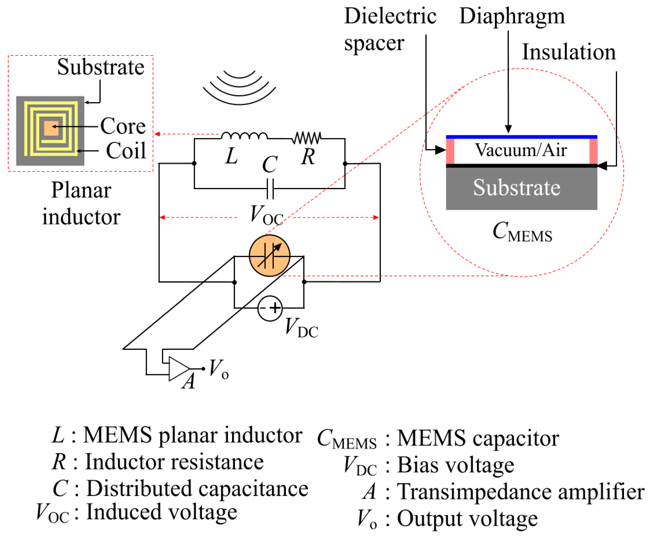
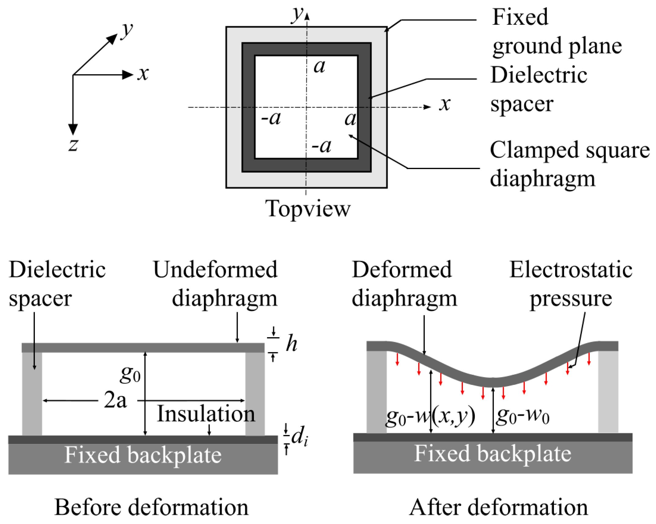
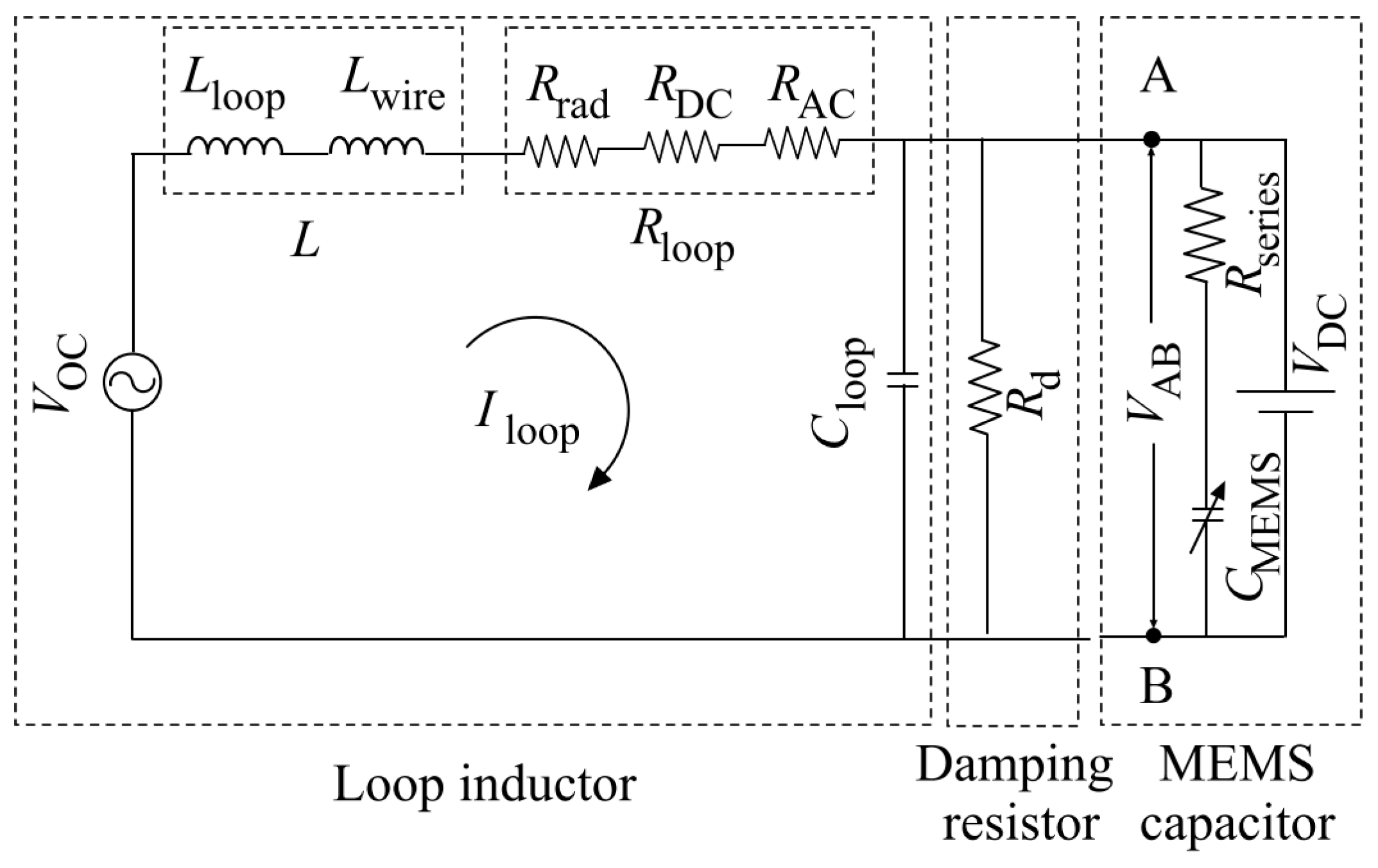
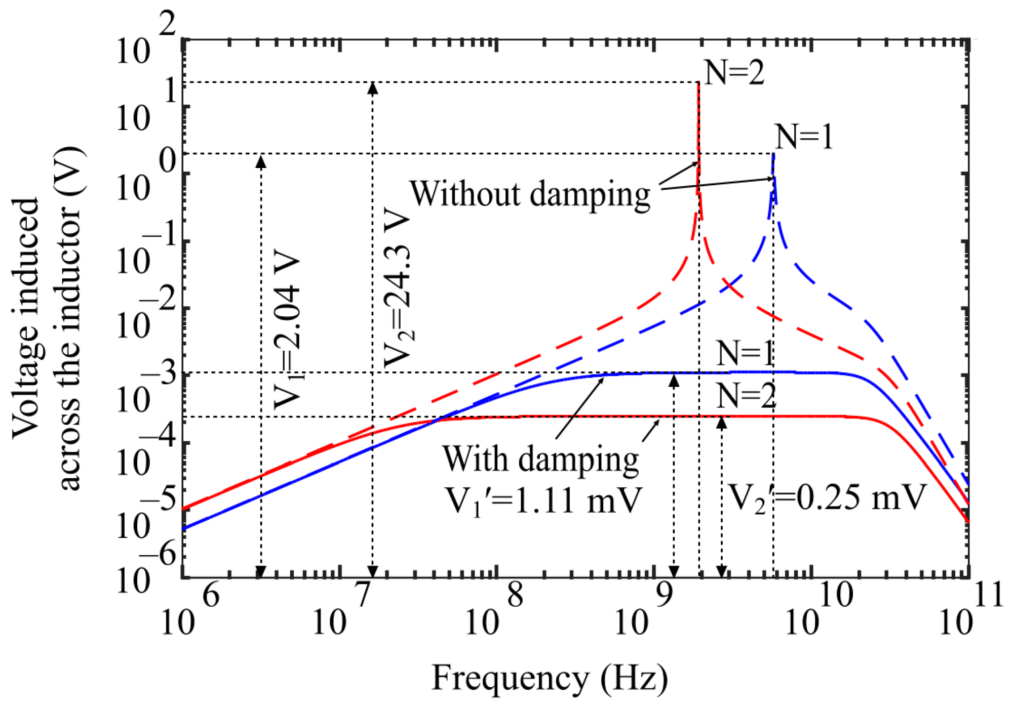
| Parameter | Value | Unit |
|---|---|---|
| Sensor footprint area | 970 × 970 | μm2 |
| Inductor area | 970 × 970 | μm2 |
| Capacitor area | 150 × 150 | μm2 |
| UWB frequency range | 3.1–10.6 | GHz |
| DC bias | 0.1 | V |
| Sensitivity | 4.5 aF/0.8 µA |
| Parameter | Value | Unit |
|---|---|---|
| Total equivalent loop area | 970 × 970 | μm2 |
| Total inductance, | 58.13 | pH |
| Gap between the sub-loops, | 5 | µm |
| Square-loop sidelength, | 60 | µm |
| Number of turns, | 1 | - |
| Width of the conductor, | 1 | µm |
| Number of sub-loops, | 225 (15 × 15) | - |
| Thickness of the conductor, | 1 | µm |
| Sub loop inductance, | 13.07 | nH |
| Conductor material | Gold | |
| Core material | Fe-Co-B | |
| Substrate | HPFS™ |
| Parameter | Value | Unit |
|---|---|---|
| Diaphragm side length, | 150 | µm |
| Diaphragm thickness (Gold), | 200 | nm |
| Dielectric spacer thickness, | 200 | nm |
| Insulation layer thickness, | 50 | nm |
| Pull-in voltage, | 0.132 | V |
| Resonant frequency, | 45.75 | kHz |
| Tuning range, | 1.68:1 | - |
| Zero bias capacitance range | 1–2 | pF |
| Capacitance change resolution | 1 | aF |
| Substrate | HPFS™ |
| Property | BCB | Gold | Unit |
|---|---|---|---|
| Young’s modulus, | 2.9 | 79 | GPa |
| Poisson ratio, | 0.34 | 0.44 | - |
| Density, | 1050 | 19,300 | Kg/m3 |
| Relative permittivity, εr | 2.65 | 6.9 | - |
Publisher’s Note: MDPI stays neutral with regard to jurisdictional claims in published maps and institutional affiliations. |
© 2021 by the authors. Licensee MDPI, Basel, Switzerland. This article is an open access article distributed under the terms and conditions of the Creative Commons Attribution (CC BY) license (https://creativecommons.org/licenses/by/4.0/).
Share and Cite
Vejella, S.; Chowdhury, S. A MEMS Ultra-Wideband (UWB) Power Sensor with a Fe-Co-B Core Planar Inductor and a Vibrating Diaphragm Capacitor. Sensors 2021, 21, 3858. https://doi.org/10.3390/s21113858
Vejella S, Chowdhury S. A MEMS Ultra-Wideband (UWB) Power Sensor with a Fe-Co-B Core Planar Inductor and a Vibrating Diaphragm Capacitor. Sensors. 2021; 21(11):3858. https://doi.org/10.3390/s21113858
Chicago/Turabian StyleVejella, Sujitha, and Sazzadur Chowdhury. 2021. "A MEMS Ultra-Wideband (UWB) Power Sensor with a Fe-Co-B Core Planar Inductor and a Vibrating Diaphragm Capacitor" Sensors 21, no. 11: 3858. https://doi.org/10.3390/s21113858
APA StyleVejella, S., & Chowdhury, S. (2021). A MEMS Ultra-Wideband (UWB) Power Sensor with a Fe-Co-B Core Planar Inductor and a Vibrating Diaphragm Capacitor. Sensors, 21(11), 3858. https://doi.org/10.3390/s21113858


