1. Introduction
Temperature sensors have been increasingly demanded in various applications such as military, aerospace, scientific research, industry, agriculture, medicine, transportation and so on. Based on the sensory device (CMOS, BJT or resistor) and the measured signal type (voltage, current, frequency, delay time, phase shift or bandwidth), they can be implemented in various ways [
1,
2,
3,
4,
5,
6,
7,
8,
9,
10,
11,
12,
13,
14,
15,
16,
17,
18,
19,
20,
21,
22]. In this paper, we have chosen a time domain CMOS temperature sensor by considering the following factors.
First, measuring something is to represent it by using a ratio of two quantities, i.e., one is to be measured and the other is to be a reference. For example, the height of a person can be represented by a multiple of foot length as shown in
Figure 1. So, we need both the person and the reference foot length to measure the height. Even when the height is measured in a metric system, we also need both the person and the reference meter.
Second, measuring temperature by using a temperature sensor does not mean that we can directly measure temperature itself. What we can really measure by using a temperature sensor are the voltage or current signals or the frequencies or delay times which are one-to-one matched to the temperature.
Third, as CMOS process technology improves, the supply voltage is getting lower and lower and the clock speed is getting higher and higher, which means that the voltage resolution is degraded, whereas the time resolution is improved. This trend has naturally made time domain signal-based circuits more attractive than ever before.
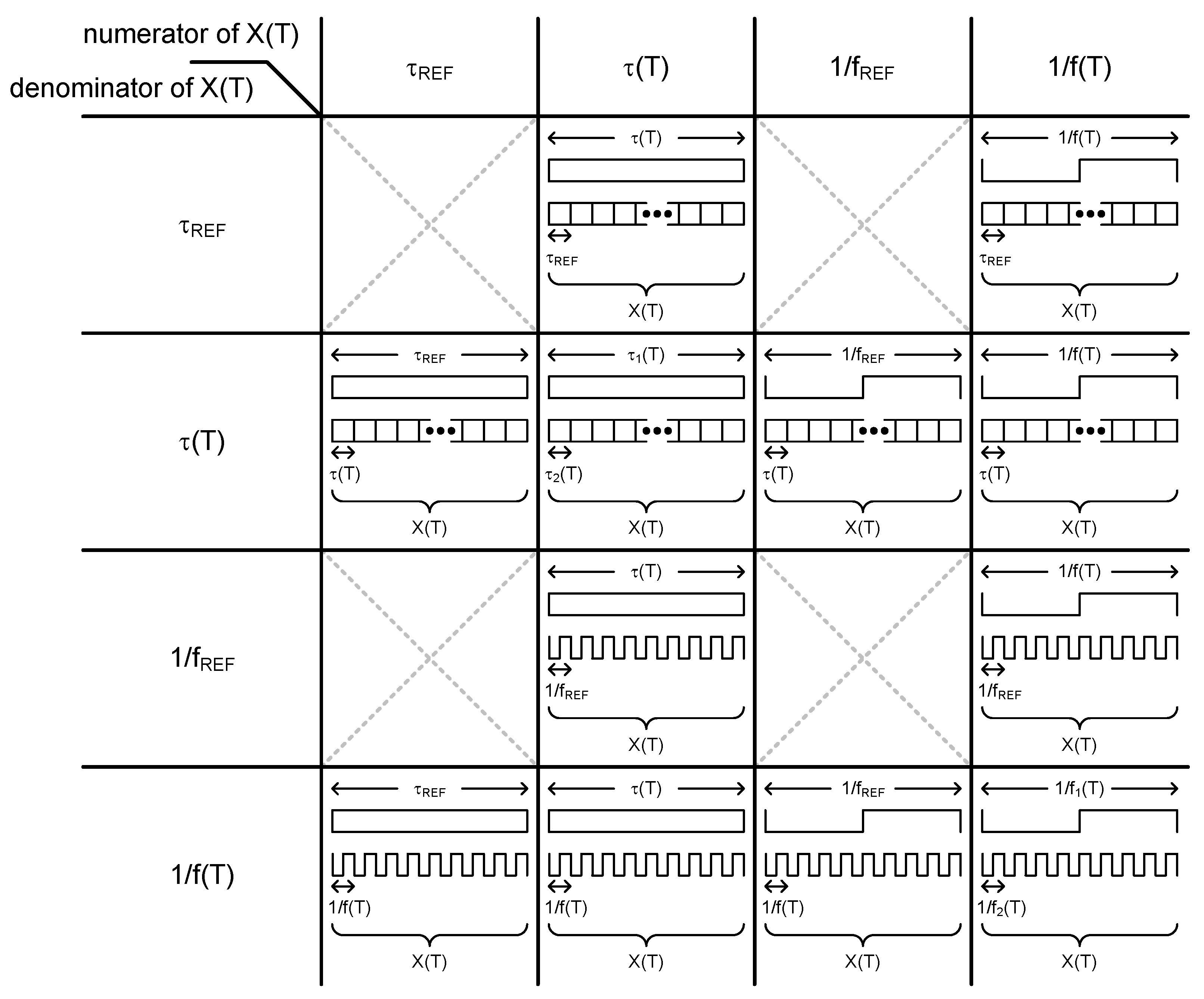
Thus, in this paper we present a new type of time domain CMOS temperature sensor which can estimate temperature by measuring a frequency and a delay time. As summarized in
Figure 2, a time domain temperature sensor can be implemented by choosing one among 12 types of operational principles. These operational principles have been categorized as shown in the figure based on the temperature estimation function, X(T), which is, in this paper, defined as the ratio of two quantities chosen from τ
REF, τ(T), 1/f
REF and 1/f(T). Here, T is the temperature and τ
REF is defined as a temperature-independent reference delay time of a delay cell or a delay line, and τ(T) is defined as a temperature-dependent delay time of a delay cell or a delay line. Similarly, f
REF is defined as a temperature-independent reference frequency of an oscillator or a clock signal, and f(T) is defined as a temperature-dependent frequency of an oscillator or a clock signal. If we arbitrarily choose two quantities from these four different kinds of time domain signals and put them into the numerator and denominator of X(T), respectively, overall 16 types of operational principles can theoretically exist, as shown in
Figure 2. However, if the two quantities are irrelevant to T at the same time, we cannot use them for temperature estimation.
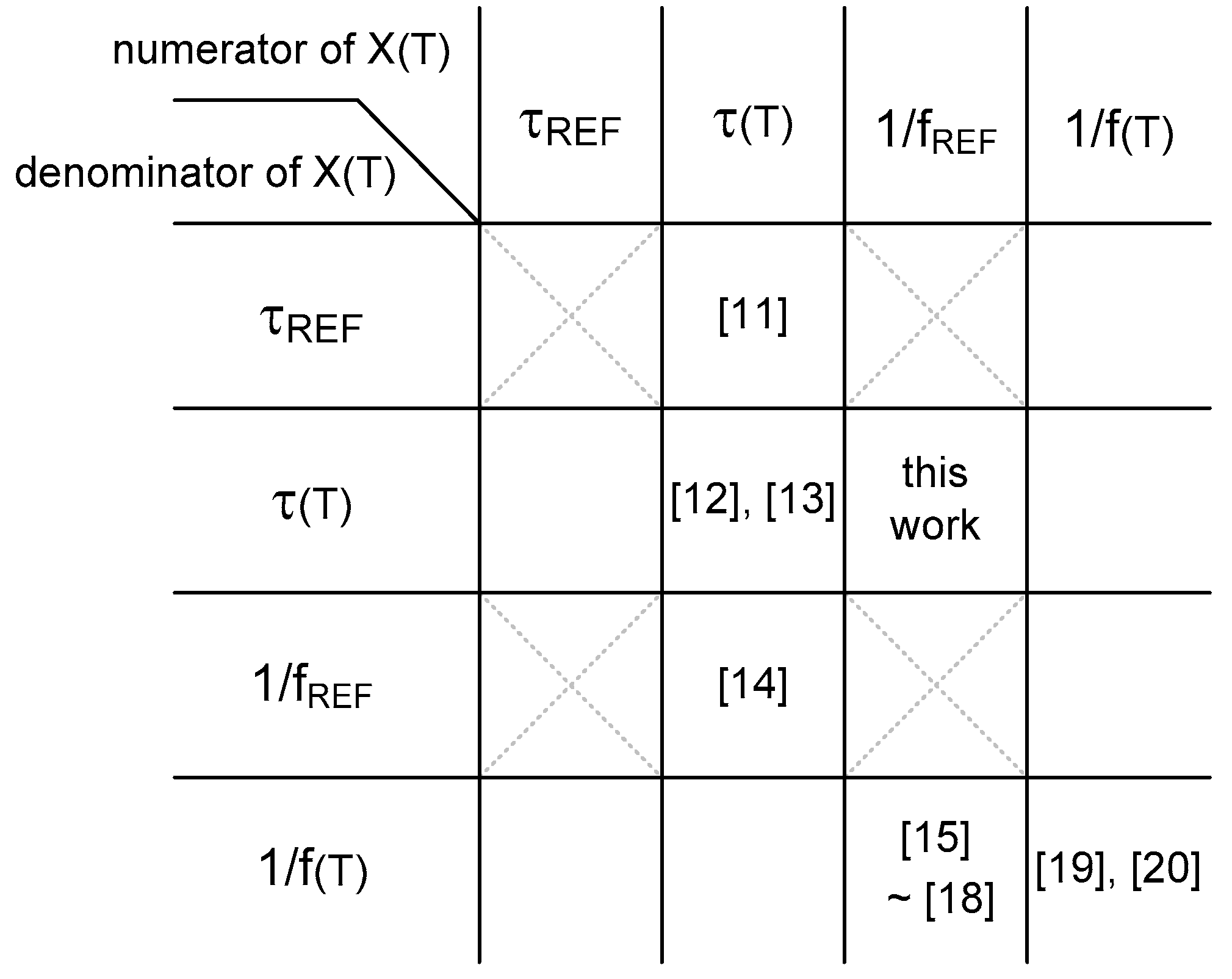
Accordingly, from the perspective of X(T), we can newly categorize the previous time domain CMOS temperature sensors, as shown in
Figure 3. In [
11], X(T) is defined as the temperature-dependent delay time, τ(T), of an open-loop delay line divided by the reference delay time, τ
REF, of a delay cell in the reference delay locked loop (DLL). A finite state machine (FSM) is used to find out the quantized digital data which corresponds to X(T). In [
12], X(T) is defined as the temperature-dependent delay time difference, τ
1(T) − τ
REF, of two delay lines divided by the other temperature-dependent delay time, τ
2(T), generated from the cyclic time-to-digital converter (TDC). In [
13], the temperature-dependent delay time, τ
1(T), of the first delay line is divided by the other temperature-dependent delay time, τ
2(T), of the fine delay cells in the second adjustable curvature-compensating reference delay line. A successive approximation register (SAR) control logic is used to obtain the quantized digital value of X(T). In [
14], the temperature-dependent delay time difference, τ
1(T) − τ
2(T), of two delay lines is divided by the reference clock period, 1/f
REF, of an external reference clock. In [
15,
16], the reference clock period, 1/f
REF, of the temperature-independent oscillator is divided by the clock period, 1/f(T), of the temperature-dependent oscillator. In [
17], the reference clock period, 1/f
REF, of an external reference clock is divided by the clock period, 1/f(T), of the temperature-dependent oscillator. In [
18], the reference clock period, 1/f
REF, of an external reference clock is first divided by the clock period, 1/f
1(T), of the temperature-dependent oscillator and then divided by the other clock period, 1/f
2(T), of the linearity controlling oscillator, respectively. Then, X(T) is obtained by taking the difference between them, i.e., X(T) = 1/f
REF/1/f
1(T) − 1/f
REF/1/f
2(T). In [
19,
20], X(T) is defined as the first clock period, 1/f
1(T), of the temperature-dependent oscillator divided by the second clock period, 1/f
2(T), of the other temperature-dependent oscillator.
In addition to the aforementioned works shown in
Figure 3, we can also design a different type of time domain CMOS temperature sensor based on the other operational principle. In this paper, we present a new type of time domain CMOS temperature sensor based on X(T) which is defined as X(T) = 1/f
REF/τ(T), as shown in
Figure 3. By choosing X(T) = 1/f
REF/τ(T), we can obtain a relatively fast temperature conversion rate since the temperature sensor has τ(T) in the denominator of X(T) and does not need to count large numbers as do the other kinds of temperature sensors, which have 1/f(T) or 1/f
REF in the denominator of X(T). Compared to [
11,
12,
13], this temperature sensor also does not need dual delay lines, since it has τ(T) only in the denominator of X(T).
This paper is organized as follows. In
Section 2, we present the architecture and the operational principle of the implemented time domain CMOS temperature sensor. We also discuss some major aspects closely related to the performance of the temperature sensor.
Section 3 explains the circuits of the main building blocks and
Section 4 shows the measured results and compares the performance with the previous works. The conclusion is given in
Section 5.
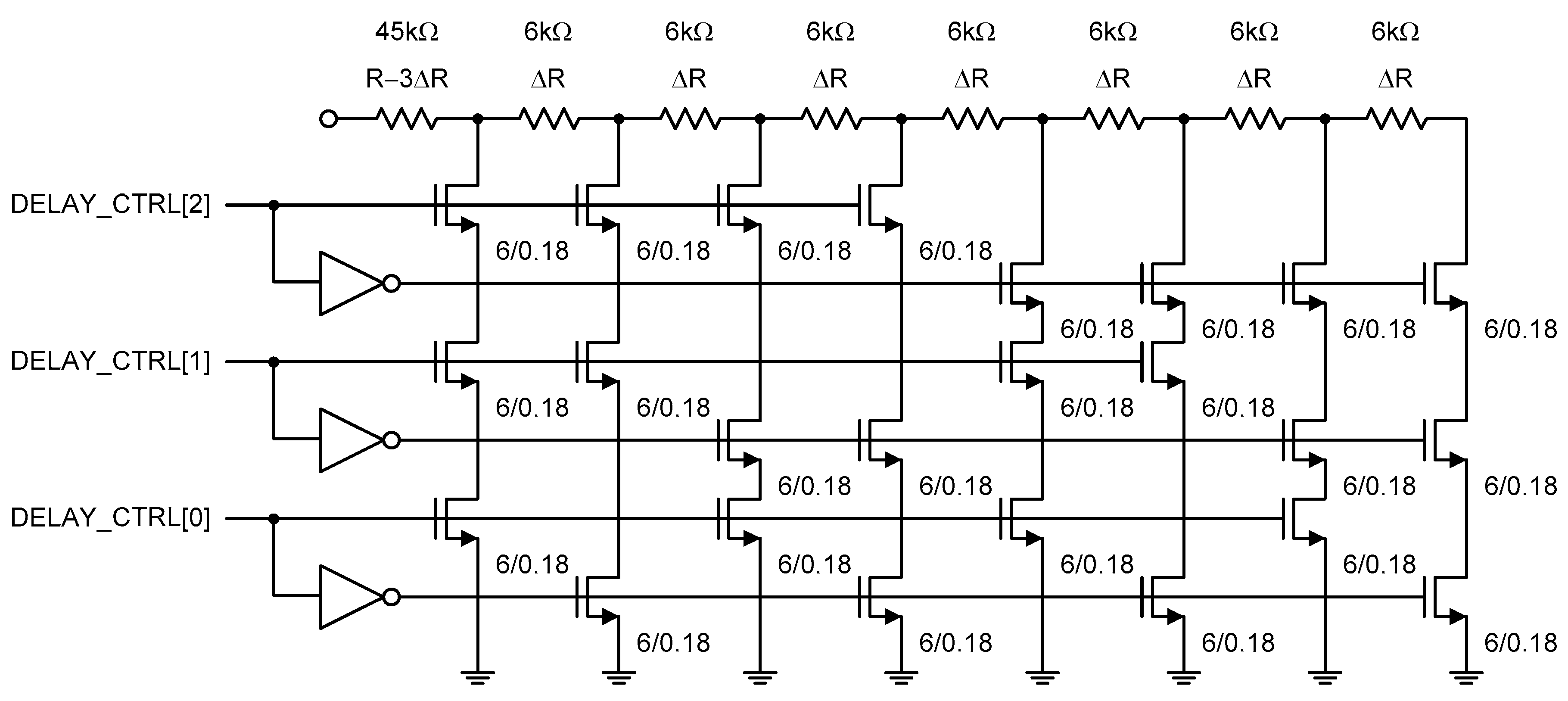
2. Architecture
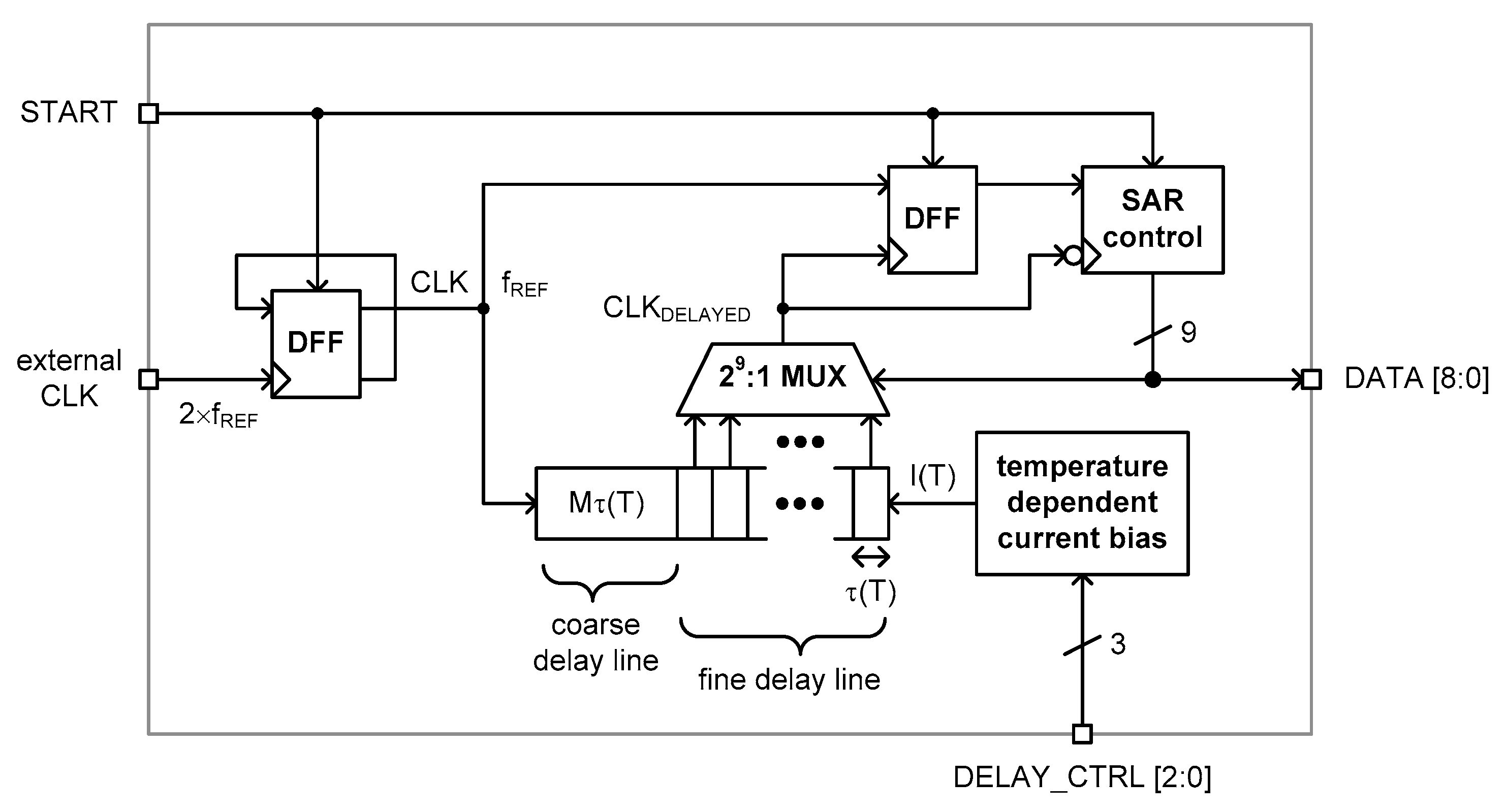
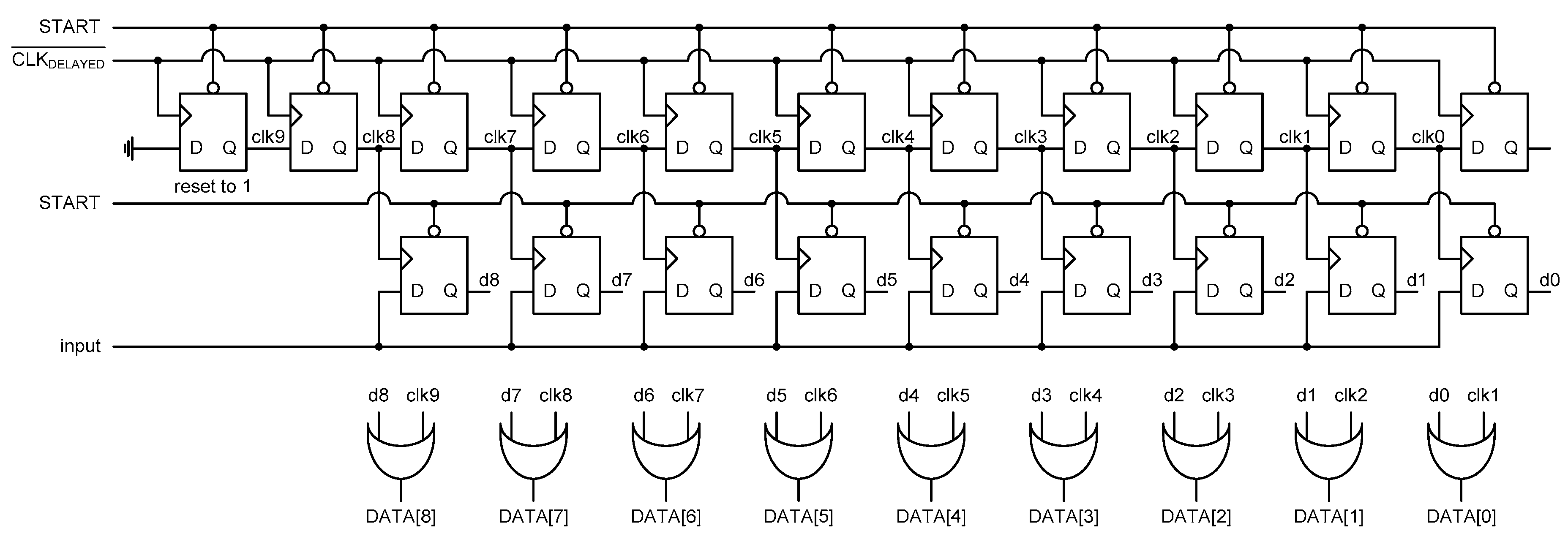
Figure 4 shows the architecture of the proposed time domain CMOS temperature sensor. This temperature sensor consists of a temperature-dependent current bias circuit, a coarse delay line, a fine delay line including 2
9 fine delay cells, a 2
9:1 MUX, a 9b SAR control logic and two DFFs.
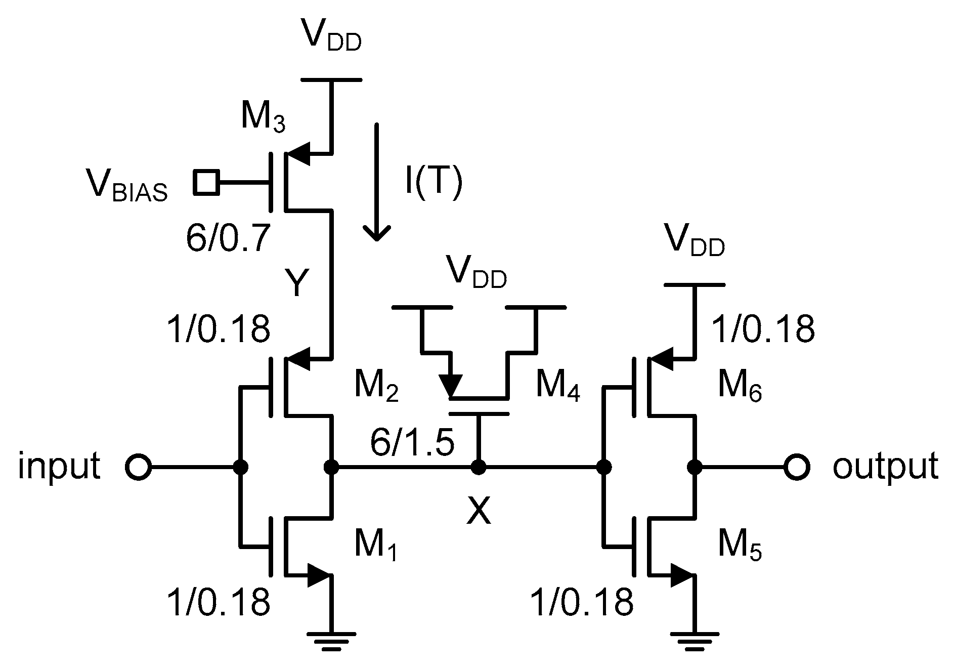
The temperature-dependent current bias circuit generates a reference current, I(T), which is linear with the temperature. This current is fed to the coarse and fine delay lines to control the delay time of the delay lines. The delay time of the coarse delay line is designed to be about 80% of the reference clock period, 1/f
REF, and the delay time of the fine delay line varies from 0% to about 40% of 1/f
REF depending on the number of fine delay cells selected by the 2
9:1 MUX. By selecting one from 2
9 delayed clock signals, the DFF can compare both the rising edges of the original clock signal, CLK, and the delayed clock signal, CLK
DELAYED, and determine which one between CLK and CLK
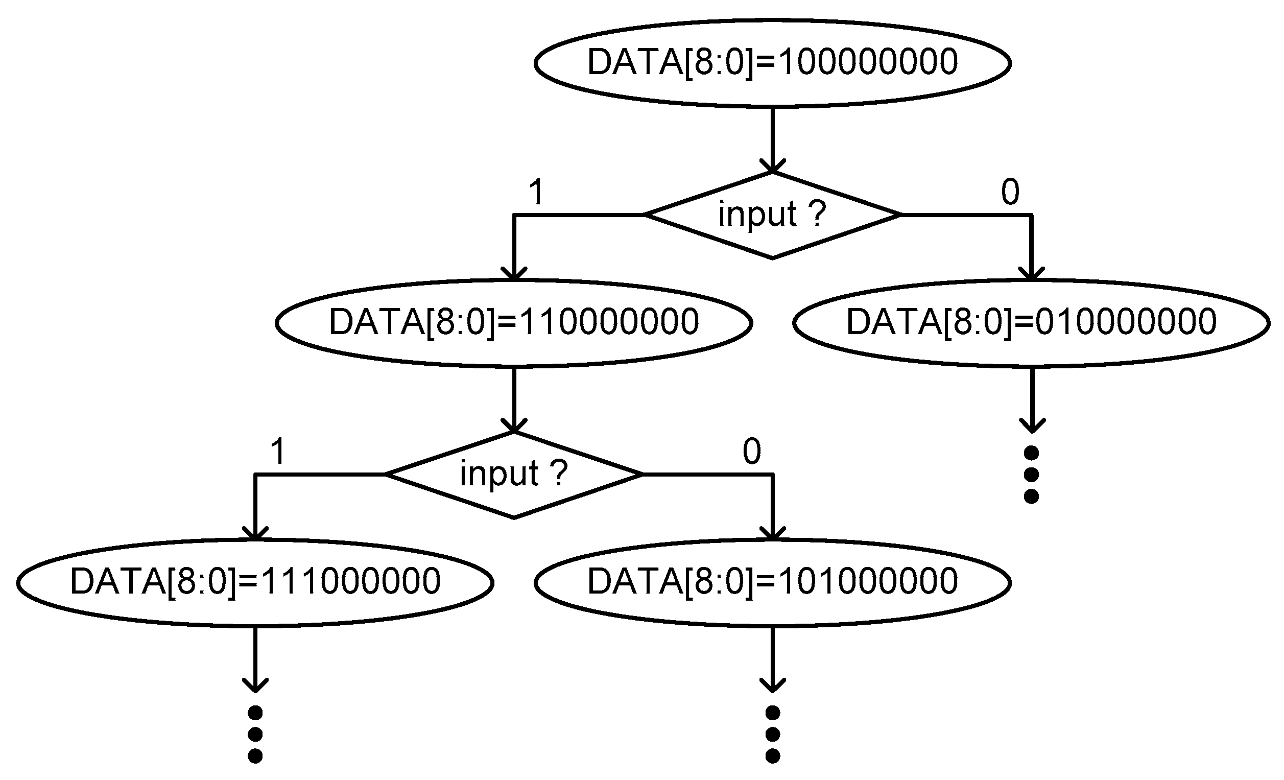
DELAYED is faster than the other. Thus, the SAR control logic can update the 9b data, DATA [8 : 0], repeatedly until the total delay time of the coarse and fine delay lines equals the reference clock period, 1/f
REF. After a complete sequence of SAR operations, Mτ(T) + X(T)τ(T) = 1/f
REF where τ(T) is the delay time of the fine delay cell, Mτ(T) is the delay time of the coarse delay line and X(T)τ(T) is the delay time of the fine delay line. This takes nine clock periods in total, i.e., 9/f
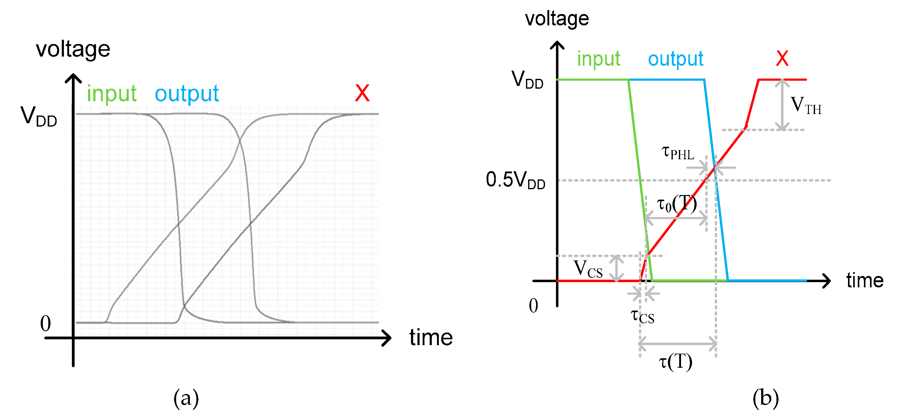
REF, for the SAR control logic to finish a complete sequence of SAR operations. Since the 9b output data, DATA[8 : 0], is equivalent to the quantized digital value of X(T), X(T) can be represented as (1). This temperature sensor is activated by the rising edge of the external trigger signal, START.
Meanwhile, the performances of this temperature sensor were closely related to the following factors: temperature linearity, process variation compensation and supply voltage insensitivity.
Having a good temperature linearity means that X(T) can be approximately expressed as X(T) = aT + b, where a and b are constants. If X(T) is linear with T, then we can accurately estimate temperature by simply measuring X(T) and by using linear interpolation. Thus, selecting the most appropriate one from various sensing elements available in the standard CMOS processes such as mobility, threshold voltage, resistance and so on, is important for good temperature linearity. Among them, mobility has relatively poor temperature linearity and threshold voltage is not easy to manipulate [
11,
12,
13,
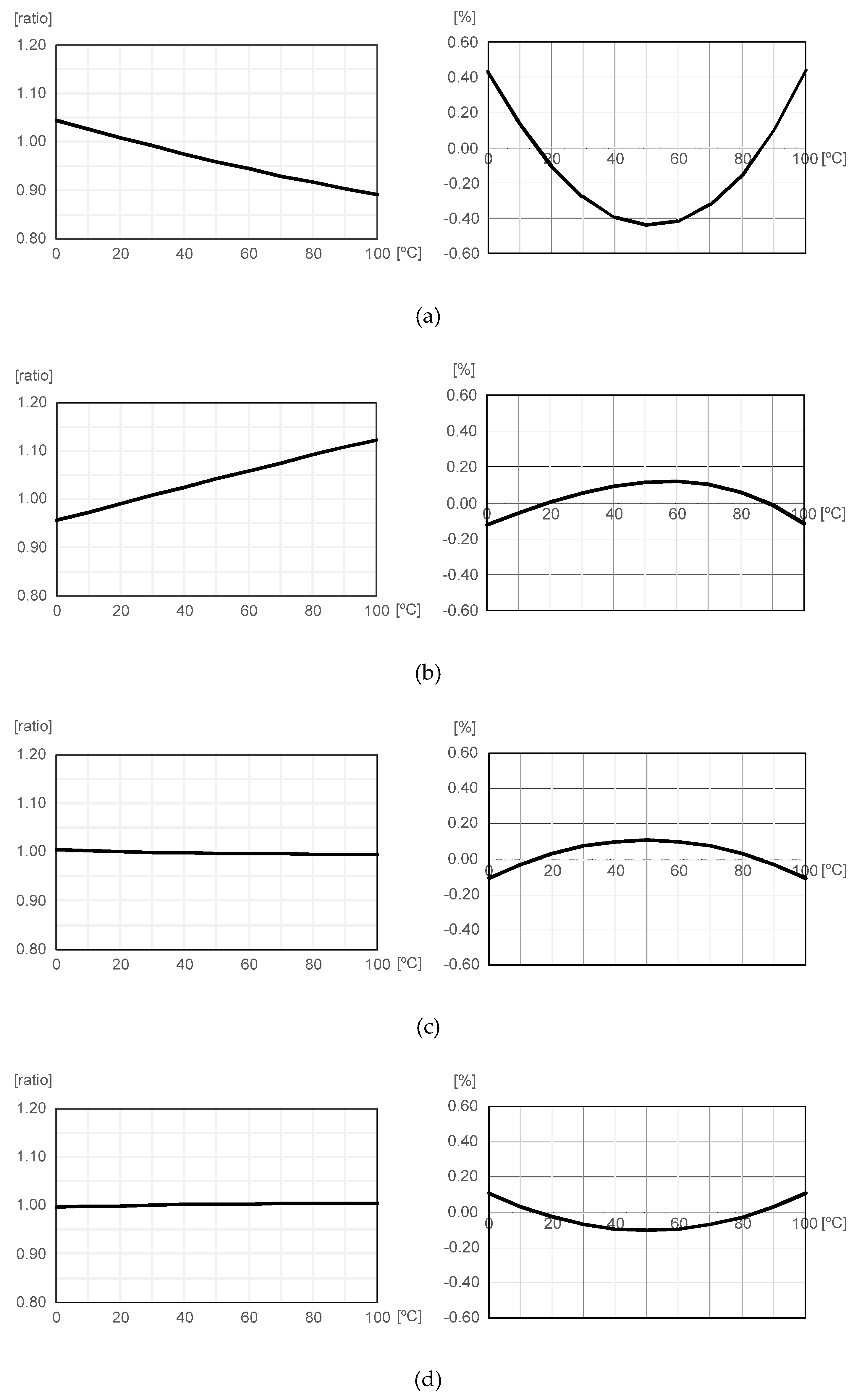
14]. Since poly resistors have relatively good temperature linearity and are easy to manipulate, we simulated the temperature linearity of n-type and p-type poly resistors as summarized in
Figure 5. In this figure, R
N(T) and R
P(T) are the resistances of n-type and p-type poly resistors, respectively. Here, the temperature-dependent variation was normalized with respect to the value measured at 25 °C and the linearity error was defined as the deviation (%) from the linear fit of the values of R(T) or 1/R(T) over the range of 0 to 100 °C. As a sensing element, we chose 1/R
N(T) in this work because R
P(T) and 1/R
P(T) were useless because they were almost constant over the range of 0 to 100 °C as shown in
Figure 5c,d. Between 1/R
N(T) and R
N(T), 1/R
N(T) had better temperature linearity than R
N(T), as shown in
Figure 5a,b. Over the range of 0 °C to 100 °C, 1/R
N(T) changed by up to 16% and had the low linearity error of ±0.12%, as shown in
Figure 5b.
Since the process corner is determined during chip fabrication, the chip characteristic is time-invariant after chip-out. That is, once we know the values of a and b in X(T) = aT + b, we can use them repeatedly for temperature estimation thereafter. Thus, we needed to carry out two-point calibration to find out the values of a and b. Specially, only if X(T) = aT, or in other words, b = 0, one-point calibration may be used for process variation compensation.
The values of a and b are actually affected if the supply voltage is shifted from its nominal value. To suppress the supply voltage sensitivity, we can choose one of the following options. The first option is to use an additional regulator for the temperature sensor [
2,
17,
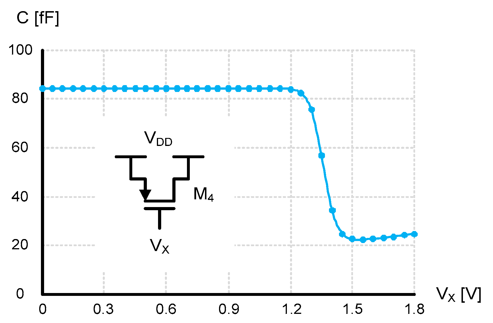
21]. The second option is to carefully devise a supply voltage-insensitive architecture such that the values of a and b are independent of the supply voltage variation. For this purpose, we can make the numerator and the denominator of X(T) equally affected by the supply voltage variation or not affected by the supply voltage variation at all. In this paper, we tried to make the numerator and the denominator of X(T) be as little affected by the supply voltage variation as possible.
4. Measurements
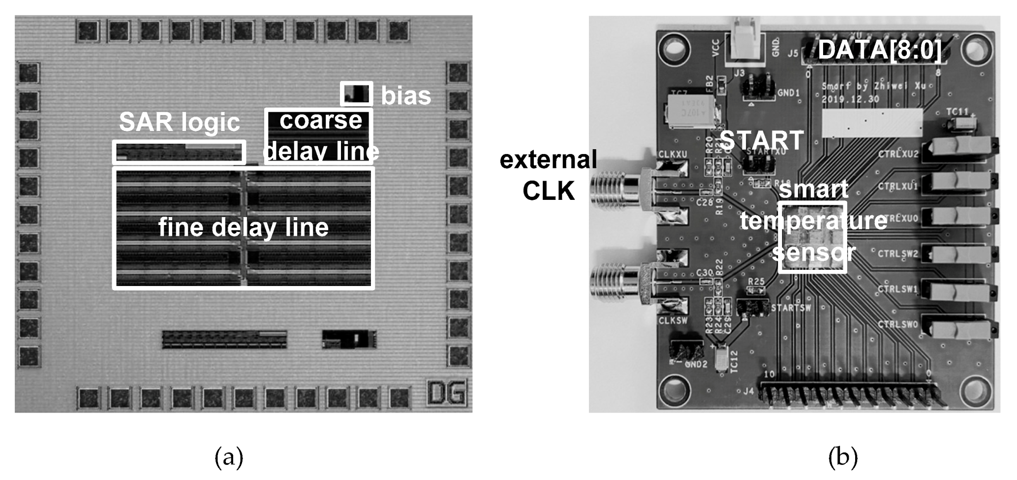
The proposed temperature sensor was implemented in a standard 0.18 μm 1P6M bulk CMOS process with general V
TH transistors.
Figure 13 shows the die photo and the FR4 PCB. The active die area was 0.432 mm
2. It occupied a relatively large area because the fine delay line contained as many as 2
9 fine delay cells for a temperature resolution as low as 0.49 °C while covering up more than 0 to 100 °C of the temperature range with margins. Thus, the die area can be reduced if the temperature resolution and temperature range requirements are mitigated.
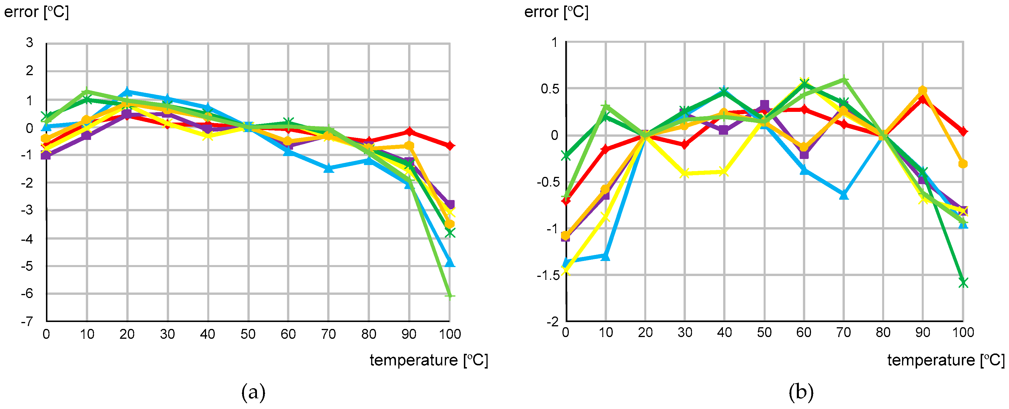
Figure 14 shows the measured temperature error over the range of 0 to 100 °C after one-point and two-point calibrations, respectively. The temperature error was measured with seven different temperature sensor chips in the temperature chamber, JEIO TC3-ME-025. For measurement accuracy, a PT100 RTD sensor (OMEGA PR-20 with DP32PT) was used as a reference. The measured temperature error varied from −6.1 to + 1.3 °C after one-point calibration at 50 °C and from −1.6 to +0.6 °C after two-point calibration at 20 and 80 °C.
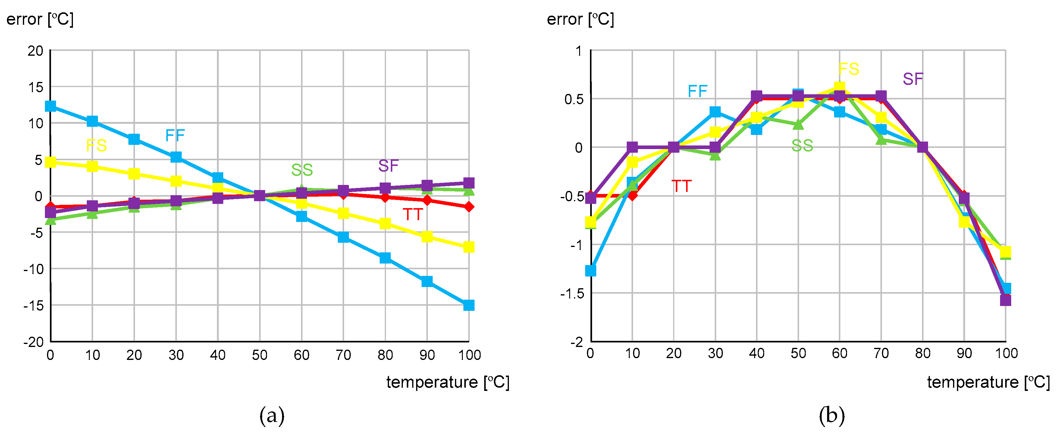
Figure 15 shows the simulated temperature error after one-point and two-point calibrations, respectively. For the process corners, TT, FS, SF, FF and SS, the simulated temperature error varied from −15.0 to + 12.3 °C after one-point calibration at 50 °C and from −1.6 to +0.6 °C after two-point calibration at 20 and 80 °C. This result agrees well with the derived Equation (6) in that X(T) is represented as aT + b and thus, we needed two-point calibration to compensate for the process variations in a and b.
The supply voltage sensitivity was measured as low as 0.085 °C/mV at 27 °C while V
DD varied from 1.65 to 1.95 V, as shown in
Figure 16. From (6), X(T) is ideally independent of V
DD because it is not a function of V
DD at all. However, the X(T) of (6) was derived under the assumption that τ
CS and τ
PHL are much smaller than τ
0(T), and V
CS is also much smaller than V
DD, respectively. Since τ
CS, τ
PHL and V
CS are very small but not zero, X(T) is slightly affected by V
DD. To reduce the supply voltage sensitivity, we canceled out V
DD in (5) by carefully designing I(T) to also be linear with V
DD, as shown in (2).
The reference clock frequency, f
REF, was 225 kHz. Since the temperature sensor operates based on the 9b SAR control logic, the conversion rate was 25 kHz and the energy efficiency was 7.2 nJ/sample.
Figure 17 shows the power consumption breakdown at 25 °C. Sixty-three percent of the total power was consumed by the temperature-dependent current bias circuit and 32% was consumed by the coarse and fine delay lines.
Table 1 compares the implemented temperature sensor with the previous time domain CMOS temperature sensors implemented in 0.13 μm or 0.18μm CMOS technologies. Compared to previous works, this temperature sensor had a relatively fast conversion rate.


