Toward the Super Temporal Resolution Image Sensor with a Germanium Photodiode for Visible Light

 , ,
, , 
Abstract
1. Introduction
2. Definitions of Temporal Resolution and Tools for Analyses
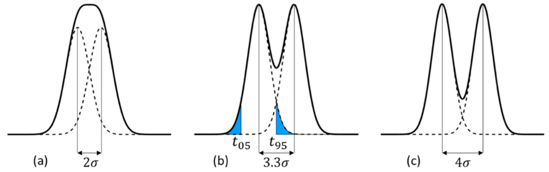
2.1. Criteria for Temporal Resolution
2.2. Temporal Resolution Based on DDF Models
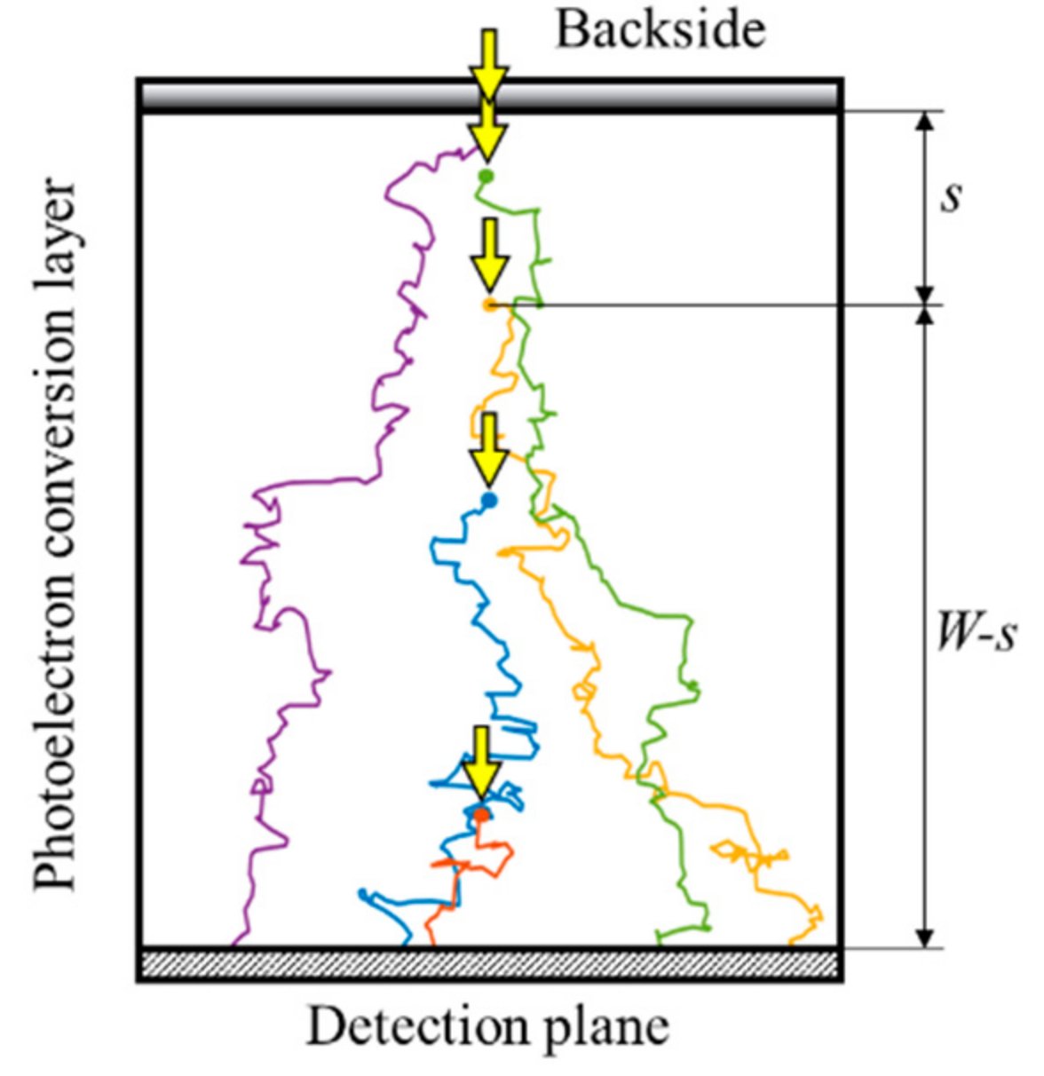
2.3. Monte Carlo Simulation Codes
3. Numerical Analyses
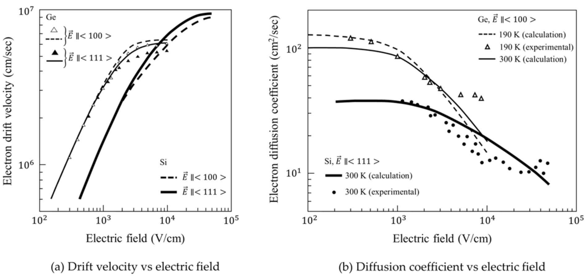
3.1. Model Parameters
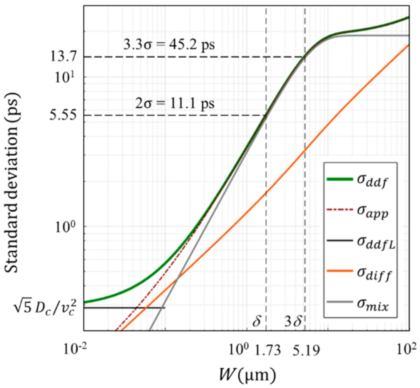
3.2. Analysis for Si PD
- there are three ranges: the mixing (drift) effect is dominant for , which covers the whole practically meaningful range, and the diffusion effect is dominant for the very thin range and for the very thick range (not drawn);
- for , the approximate expressions almost perfectly agree with the exact solution from the DDF model; for , the discrepancy increases and the DDF model asymptotically converges to a constant value, ;
- the range used in practical applications, , is included in the drift-dominant range as concluded in our previous paper [1];
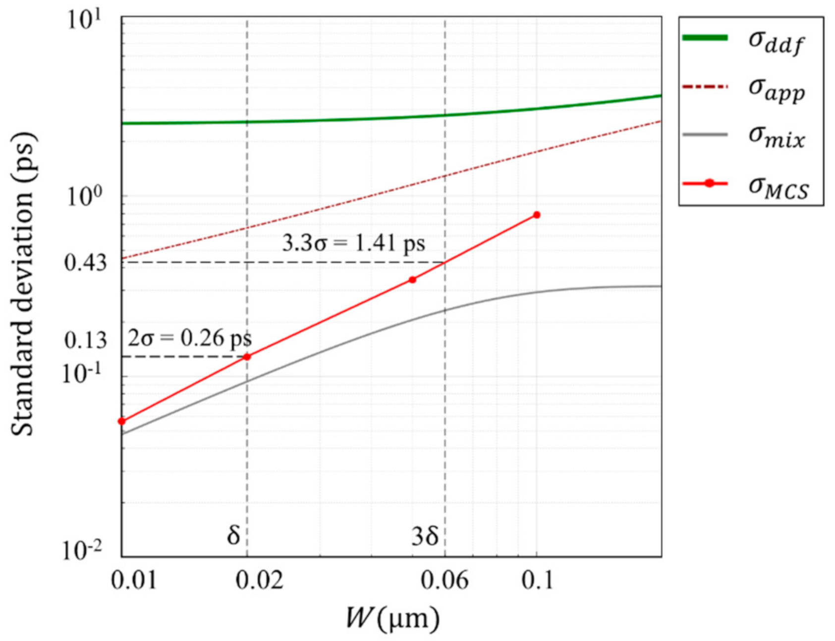
- The theoretical temporal resolution limit for is , and the practical limit for is .
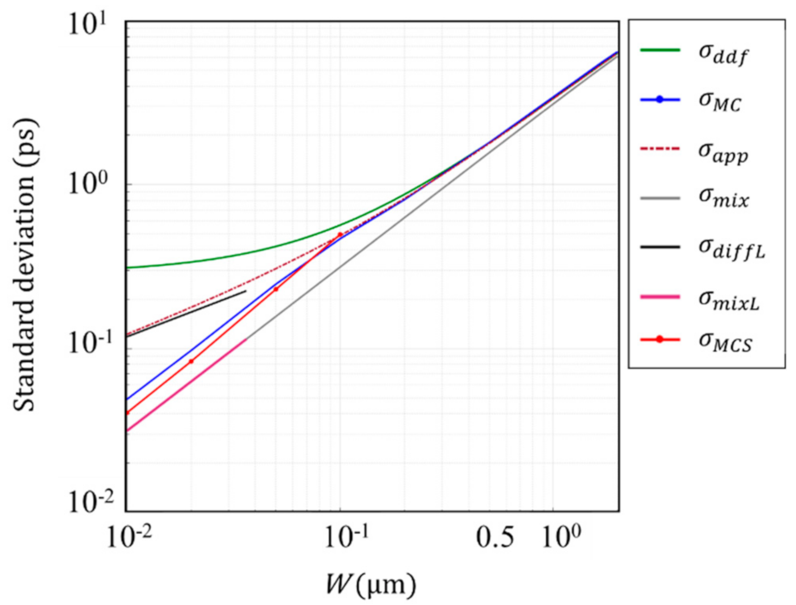
- the Monte Carlo simulation shows that monotonically decreases when the thickness of the photodiode decreases, while the numerical solution of the DDF model converges to a constant value for an infinitesimal thickness;
- for , departs from , and goes along the approximate expression
- for from our inhouse MC simulation code departs from and, for , it becomes parallel to the mixing (drift) component with the slope proportional to , suggesting that the motion of the signal electrons converges to a ballistic motion (see Appendix C).
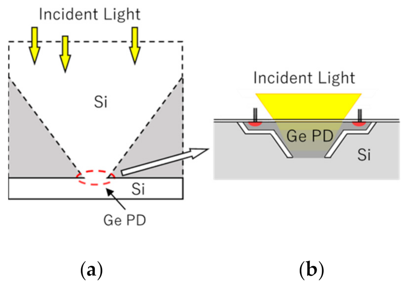
3.3. Super Temporal Resolution Limit for a Ge PD
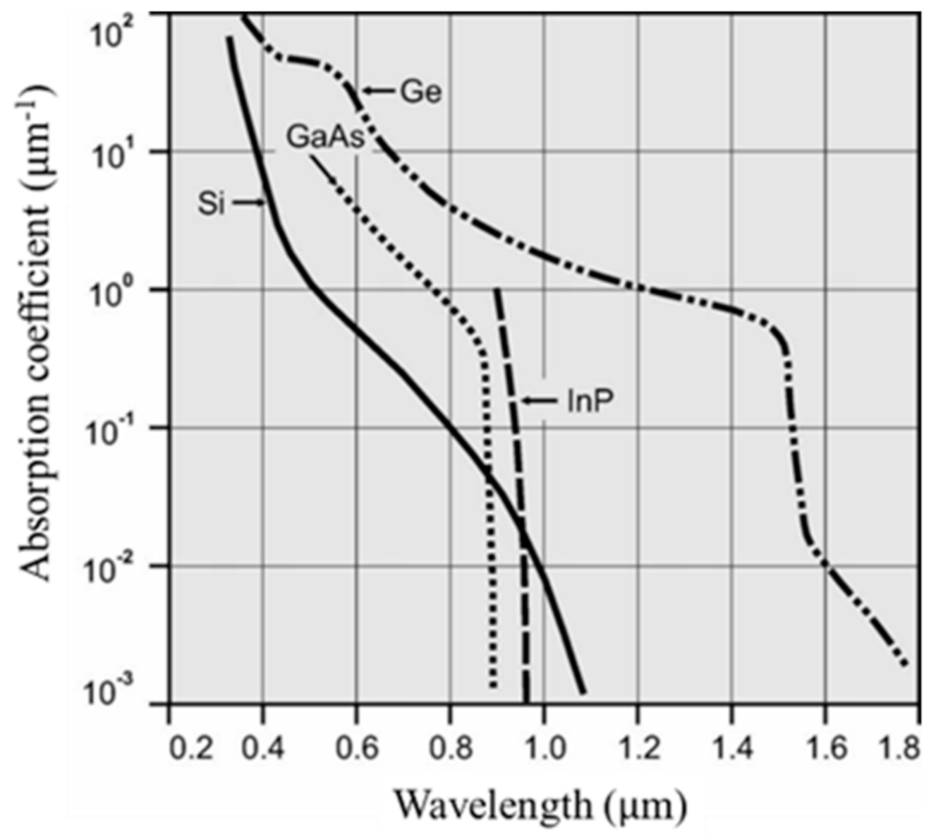
3.4. Toward Super Temporal Resolution through SWIR Imaging
4. Dark Current
5. Concluding Remarks
5.1. Conclusions
5.2. Remarks
Author Contributions
Funding
Conflicts of Interest
List of Symbols
| Symbol | Description |
| Absorption rate of incident light | |
| Penetration depth of incident light | |
| Drift velocity at saturation | |
| Diffusion coefficient at the drift velocity saturated | |
| Mean | |
| Theoretical temporal resolution limit | |
| Practical temporal resolution | |
| Standard deviation of the arrival time of signal electrons | |
| Standard deviation of the drift-diffusion-flux model | |
| Limit of the standard deviation of the drift-diffusion-flux model | |
| Standard deviation of the approximation model | |
| Standard deviation of the mixing component | |
| Standard deviation of the diffusion component | |
| for the infinitesimal thickness of the photodiode | |
| for the infinitesimal thickness of the photodiode | |
| for the infinitesimal thickness of the photodiode | |
| Standard deviation calculated with the inhouse MC simulation code | |
| Standard deviation calculated with the Sentaurus MC simulation code | |
| Thickness of the sensor | |
| for the theoretical temporal resolution limit | |
| for the practical temporal resolution limit |
Appendix A. Exact Formulation of the Temporal Resolution

| Strict Expression | ||
|---|---|---|
| The Gaussian drift-diffusion equation for a single pulse | ||
| The flux passing a detection plane | ||
| The penetration depth distribution | ||
| Convolution of and | ||
| The 0th moment (Absorption rate) | ||
| The 1st moment | ||
| The 2nd moment | ||
| Variance | ||
| Temporal resolution | ||
| Normalized parameters | ||
Appendix B. An Explicit Approximate Expression for the Temporal Resolution
| Approximation Formula | Solutions | Asymptotic Expressions | |
|---|---|---|---|
| The penetration depth distribution | |||
| Absorption rate | |||
| Average arrival time | |||
| Mixing component of variance | |||
| Diffusion component of variance | |||
| Variance | |||
| Approximation for a whole thickness | perfectly fits ( and are in Appendix A) | ||
| Temporal resolution | |||
| Normalized parameters | |||
Appendix C. Derivations of the Asymptotic Expressions
Appendix D. A Method to Estimate the Standard Deviation by Using the Sentaurus MC Simulation Code
- (1)
- is the number of all generated electrons, including electrons taking paths which are not our target, especially, the number of electrons absorbed at the source electrode and injected from another electrode,
- (2)
- is a random number.

References
- Etoh, T.G.; Nguyen, A.Q.; Kamakura, Y.; Shimonomura, K.; Le, T.Y.; Mori, N. The theoretical highest frame rate of silicon image sensors. Sensors 2017, 17, 483. [Google Scholar] [CrossRef] [PubMed]
- Shiraga, H.; Miyanaga, N.; Heya, M.; Nakasuji, M.; Aoki, Y.; Azechi, H.; Yamanaka, T.; Mima, K. Ultrafast two-dimensional x-ray imaging with x-ray streak cameras for laser fusion research. Rev. Sci. Instrum. 1997, 68, 745–749. [Google Scholar] [CrossRef]
- Kubota, T.; Awatsuji, Y. Observation of light propagation by holography with a picosecond pulsed laser. Opt. Lett. 2002, 27, 815–817. [Google Scholar] [CrossRef] [PubMed]
- Kubota, T.; Komai, K.; Yamagiwa, M.; Awatsuji, Y. Moving picture recording and observation of three-dimensional image of femtosecond light pulse propagation. Opt. Express 2007, 15, 14348–14354. [Google Scholar] [CrossRef]
- Kakue, T.; Tosa, K.; Yuasa, J.; Tahara, T.; Awatsuji, Y.; Nishio, K.; Ura, S.; Kubota, T. Digital Light-in-Flight Recording by Holography by Use of a Femtosecond Pulsed Laser. IEEE J. Sel. Top. Quantum Electron. 2012, 18, 479–485. [Google Scholar] [CrossRef]
- Nagel, S.R.; Hilsabeck, T.J.; Bell, P.M.; Bradley, D.K.; Ayers, M.J.; Barrios, M.A.; Felker, B.; Smith, R.F.; Collins, G.W.; Jones, O.S.; et al. Dilation X-ray imager a new/faster gated X-ray imager for the NIF. Rev. Sci. Instrum. 2012, 83, 10E116. [Google Scholar] [CrossRef]
- Nakagawa, K.; Iwasaki, A.; Oishi, Y.; Horisaki, R.; Tsukamoto, A.; Nakamura, A.; Hirosawa, K.; Liao, H.; Ushida, T.; Goda, K.; et al. Sequentially timed all-optical mapping photography (STAMP). Nat. Photonics 2014, 8, 695–700. [Google Scholar] [CrossRef]
- Gao, L.; Liang, J.; Li, C.; Wang, L.V. Single-shot compressed ultrafast photography at one hundred billion frames per second. Nature 2014, 516, 74–77. [Google Scholar] [CrossRef]
- Cai, H.; Zhao, X.; Liu, J.; Xie, W.; Bai, Y.; Lei, Y.; Liao, Y.; Niu, H. Dilation framing camera with 4 ps resolution. Apl Photonics 2016, 1, 16101. [Google Scholar] [CrossRef]
- Suzuki, T.; Hida, R.; Yamaguchi, Y.; Nakagawa, K.; Saiki, T.; Kannari, F. Single-shot 25-frame burst imaging of ultrafast phase transition of Ge2Sb2Te5 with a sub-picosecond resolution. Appl. Phys. Express 2017, 10, 92502. [Google Scholar] [CrossRef]
- Liang, J.; Ma, C.; Zhu, L.; Chen, Y.; Gao, L.; Wang, L.V. Single-shot real-time video recording of a photonic Mach cone induced by a scattered light pulse. Sci. Adv. 2017, 3, e1601814. [Google Scholar] [CrossRef] [PubMed]
- Inoue, T.; Matsunaka, A.; Funahashi, A.; Okuda, T.; Nishio, K.; Awatsuji, Y. Spatiotemporal observations of light propagation in multiple polarization states. Opt. Lett. 2019, 44, 2069–2072. [Google Scholar] [CrossRef] [PubMed]
- Kim, T.; Liang, J.; Zhu, L.; Wang, L.V. Picosecond-resolution phase-sensitive imaging of transparent objects in a single shot. Sci. Adv. 2020, 6, eaay6200. [Google Scholar] [CrossRef] [PubMed]
- Wang, P.; Liang, J.; Wang, L.V. Single-shot ultrafast imaging attaining 70 trillion frames per second. Nat. Commun. 2020, 11, 2091. [Google Scholar] [CrossRef]
- 31st International Congress of High-Speed Imaging and Photonics. Available online: https://www.ile.osaka-u.ac.jp/research/fps/ichsip-31/invited/index.html (accessed on 23 November 2020).
- Etoh, T. A high-speed video camera operating at 4500 fps. J. Inst. Telev. Eng. Jpn. 1992, 46, 543–545. (In Japanese) [Google Scholar]
- Kosonocky, W.; Yang, G.; Ye, C.; Kabra, R.; Xie, L.; Lawrence, J.; Mastrocolla, V.; Shallcross, F.; Patel, V. 360 × 360-element very-high-frame-rate burst image sensor. In Proceedings of the Digest of Technical Papers, 1996 IEEE International Solid-State Circuits Conference (ISSCC), San Fransisco, CA, USA, 10 February 1996; pp. 182–183. [Google Scholar]
- Etoh, T.G.; Poggemann, D.; Ruckelshausen, A.; Theuwissen, A.; Kreider, G.; Folkerts, H.-O.; Mutoh, H.; Kondo, Y.; Maruno, H.; Takubo, K.; et al. A CCD image sensor of 1 Mframes/s for continuous image capturing 103 frames. In Proceedings of the 2002 IEEE International Solid-State Circuits Conference, Digest of Technical Papers (Cat. No.02CH37315), San Francisco, CA, USA, 7 February 2002; pp. 46–443. [Google Scholar]
- Etoh, T.G.; Nguyen, D.H.; Dao, S.V.T.; Vo, C.L.; Tanaka, M.; Takehara, K.; Okinaka, T.; van Kuijk, H.; Klaassens, W.; Bosiers, J.; et al. A 16 Mfps 165kpixel backside-illuminated CCD. In Proceedings of the 2011 IEEE International Solid-State Circuits Conference, San Francisco, CA, USA, 20–24 February 2011; pp. 406–408. [Google Scholar]
- Crooks, J.; Marsh, B.; Turchetta, R.; Taylor, K.; Chan, W.; Lahav, A.; Fenigstein, A. Kirana: A solid-state megapixel uCMOS image sensor for ultrahigh speed imaging. In Proceedings of the Sensors, Cameras, and Systems for Industrial and Scientific Applications XIV, Burlingame, CA, USA, 19 February 2013; Volume 8659, pp. 36–49. [Google Scholar]
- Tochigi, Y.; Hanzawa, K.; Kato, Y.; Kuroda, R.; Mutoh, H.; Hirose, R.; Tominaga, H.; Takubo, K.; Kondo, Y.; Sugawa, S. A Global-Shutter CMOS Image Sensor with Readout Speed of 1-Tpixel/s Burst and 780-Mpixel/s Continuous. IEEE J. Solid-State Circuits 2013, 48, 329–338. [Google Scholar] [CrossRef]
- Mochizuki, F.; Kagawa, K.; Okihara, S.; Seo, M.; Zhang, B.; Takasawa, T.; Yasutomi, K.; Kawahito, S. Single-shot 200 Mfps 5×3-aperture compressive CMOS imager. In Proceedings of the 2015 IEEE International Solid-State Circuits Conference (ISSCC), San Francisco, CA, USA, 22–26 February 2015; Volume 58, pp. 116–117. [Google Scholar]
- Claus, L.; Fang, L.; Kay, R.; Kimmel, M.; Long, J.; Robertson, G.; Sanchez, M.; Stahoviak, J.; Trotter, D.; Porter, J.L. An overview of the Ultrafast X-ray Imager (UXI) program at Sandia Labs. In Proceedings of the Target Diagnostics Physics and Engineering for Inertial Confinement Fusion IV, San Diego, CA, USA, 31 August 2015; Volume 9591, p. 95910. [Google Scholar]
- Dao, V.T.S.; Ngo, N.; Nguyen, A.Q.; Morimoto, K.; Shimonomura, K.; Goetschalckx, P.; Haspeslagh, L.; De Moor, P.; Takehara, K.; Etoh, T.G. An Image Signal Accumulation Multi-Collection-Gate Image Sensor Operating at 25 Mfps with 32 × 32 Pixels and 1220 In-Pixel Frame Memory. Sensors 2018, 18, 3112. [Google Scholar] [CrossRef]
- Etoh, T.G.; Okinaka, T.; Takano, Y.; Takehara, K.; Nakano, H.; Shimonomura, K.; Ando, T.; Ngo, N.; Kamakura, Y.; Dao, V.T.S.; et al. Light-in-flight imaging by a silicon image sensor: Toward the theoretical highest frame rate. Sensors 2019, 19, 2247. [Google Scholar] [CrossRef]
- Kuroda, R.; Suzuki, M.; Sugawa, S. Over 100 million frames per second high speed global shutter CMOS image sensor. In Proceedings of the 32nd International Congress on High-Speed Imaging and Photonics, Enschede, The Netherlands, 28 January 2019; Volume 11051, pp. 57–62. [Google Scholar]
- Hart, P.A.; Carpenter, A.; Claus, L.; Damiani, D.; Dayton, M.; Decker, F.-J.; Gleason, A.; Heimann, P.; Hurd, E.; McBride, E.; et al. First X-ray test of the Icarus nanosecond-gated camera. In Proceedings of the X-ray Free-Electron Lasers: Advances in Source Development and Instrumentation V, Prague, Czech Republic, 24 April 2019; Volume 110380, p. 110380Q. [Google Scholar]
- Ogawa, S.; Asahara, R.; Minoura, Y.; Sako, H.; Kawasaki, N.; Yamada, I.; Miyamoto, T.; Hosoi, T.; Shimura, T.; Watanabe, H. Insights into thermal diffusion of germanium and oxygen atoms in HfO2/GeO2/Ge gate stacks and their suppressed reaction with atomically thin AlOx interlayers. J. Appl. Phys. 2015, 118, 235704. [Google Scholar] [CrossRef]
- Shimura, T.; Matsue, M.; Tominaga, K.; Kajimura, K.; Amamoto, T.; Hosoi, T.; Watanabe, H. Enhancement of photoluminescence from n-type tensile-strained GeSn wires on an insulator fabricated by lateral liquid-phase epitaxy. Appl. Phys. Lett. 2015, 107, 221109. [Google Scholar] [CrossRef]
- Oka, H.; Tomita, T.; Hosoi, T.; Shimura, T.; Watanabe, H. Lightly doped n-type tensile-strained single-crystalline {GeSn}-on-insulator structures formed by lateral liquid-phase crystallization. Appl. Phys. Express 2017, 11, 1011304. [Google Scholar] [CrossRef]
- Wada, Y.; Inoue, K.; Hosoi, T.; Shimura, T.; Watanabe, H. Demonstration of mm long nearly intrinsic {GeSn} single-crystalline wires on quartz substrate fabricated by nucleation-controlled liquid-phase crystallization. Jpn. J. Appl. Phys. 2019, 58, SBBK01. [Google Scholar] [CrossRef]
- Gariepy, G.; Krstajić, N.; Henderson, R.; Li, C.; Thomson, R.R.; Buller, G.S.; Heshmat, B.; Raskar, R.; Leach, J.; Faccio, D. Single-photon sensitive light-in-fight imaging. Nat. Commun. 2015, 6, 6021. [Google Scholar] [CrossRef] [PubMed]
- Vines, P.; Kuzmenko, K.; Kirdoda, J.; Dumas, D.C.S.; Mirza, M.M.; Millar, R.W.; Paul, D.J.; Buller, G.S. High performance planar germanium-on-silicon single-photon avalanche diode detectors. Nat. Commun. 2019, 10, 1086. [Google Scholar] [CrossRef] [PubMed]
- Martinez, N.J.D.; Derose, C.T.; Brock, R.W.; Starbuck, A.L.; Pomerene, A.T.; Lentine, A.L.; Trotter, D.C.; Davids, P.S. High performance waveguide-coupled Ge-on-Si linear mode avalanche photodiodes. Opt. Express 2016, 24, 19072–19081. [Google Scholar] [CrossRef]
- Kunikiyo, T.; Takenaka, M.; Kamakura, Y.; Yamaji, M.; Mizuno, H.; Morifuji, M.; Taniguchi, K.; Hamaguchi, C. A Monte Carlo simulation of anisotropic electron transport in silicon including full band structure and anisotropic impact-ionization model. J. Appl. Phys. 1994, 75, 297–312. [Google Scholar] [CrossRef]
- Jacoboni, C.; Canali, C.; Ottaviani, G.; Quaranta, A. A review of some charge transport properties of silicon. Solid-State Electron. 1977, 20, 77–89. [Google Scholar] [CrossRef]
- Jacoboni, C.; Nava, F.; Canali, C.; Ottaviani, G. Electron drift velocity and diffusivity in germanium. Phys. Rev. B 1981, 24, 1014–1026. [Google Scholar] [CrossRef]
- Omar, M.A.; Reggiani, L. Drift velocity and diffusivity of hot carriers in germanium: Model calculations. Solid-State Electron. 1987, 30, 1351–1354. [Google Scholar] [CrossRef]
- Jones, M.H.; Jones, S.H. Optical Properties of Silicon. Available online: https://www.univie.ac.at/photovoltaik/vorlesung/ss2014/unit4/optical_properties_silicon.pdf (accessed on 23 November 2020).
- Palik, E.D. Handbook of Optical Constants of Solids; Academic Press: New York, NY, USA, 1985; Volume 1, ISBN 978-0-08-054721-3. [Google Scholar]
- Green, M.A.; Keevers, M.J. Optical properties of intrinsic silicon at 300 K. Prog. Photovolt. Res. Appl. 1995, 3, 189–192. [Google Scholar] [CrossRef]
- Optical Absorption Coefficient Calculator. Available online: https://cleanroom.byu.edu/opticalcalc (accessed on 23 November 2020).
- Nemecek, A.; Zach, G.; Swoboda, R.; Oberhauser, K.; Zimmermann, H. Integrated BiCMOS pin photodetectors with high bandwidth and high responsivity. IEEE J. Sel. Top. Quantum Electron. 2006, 12, 1469–1475. [Google Scholar] [CrossRef]
- Sentaurus Device Monte Carlo User Guide, O-2018.06; Synopsys: Mountain View, CA, USA, 2018.
- Nguyen, A.Q.; Dao, V.T.S.; Shimonomura, K.; Takehara, K.; Etoh, T.G. Toward the Ultimate High-speed Image Sensor: From 10 ns to 50 ps. Sensors 2018, 18, 2407. [Google Scholar] [CrossRef] [PubMed]


| Si | Ge | ||
|---|---|---|---|
| Wavelength | 0.55 m | 0.55 m | 1 m |
| Penetration depth | 1.73 m | 20.0 nm | 526 nm |
| Critical E-field | 25 kV/cm | 4.2 kV/cm | |
| Drift velocity | 9.19 106 cm/s | 5.8 106 cm/s | |
| Diffusion coefficient | 10.8 cm2/s | 42.5 cm2/s | |
Publisher’s Note: MDPI stays neutral with regard to jurisdictional claims in published maps and institutional affiliations. |
© 2020 by the authors. Licensee MDPI, Basel, Switzerland. This article is an open access article distributed under the terms and conditions of the Creative Commons Attribution (CC BY) license (http://creativecommons.org/licenses/by/4.0/).
Share and Cite
Ngo, N.H.; Nguyen, A.Q.; Bufler, F.M.; Kamakura, Y.; Mutoh, H.; Shimura, T.; Hosoi, T.; Watanabe, H.; Matagne, P.; Shimonomura, K.; et al. Toward the Super Temporal Resolution Image Sensor with a Germanium Photodiode for Visible Light. Sensors 2020, 20, 6895. https://doi.org/10.3390/s20236895
Ngo NH, Nguyen AQ, Bufler FM, Kamakura Y, Mutoh H, Shimura T, Hosoi T, Watanabe H, Matagne P, Shimonomura K, et al. Toward the Super Temporal Resolution Image Sensor with a Germanium Photodiode for Visible Light. Sensors. 2020; 20(23):6895. https://doi.org/10.3390/s20236895
Chicago/Turabian StyleNgo, Nguyen Hoai, Anh Quang Nguyen, Fabian M. Bufler, Yoshinari Kamakura, Hideki Mutoh, Takayoshi Shimura, Takuji Hosoi, Heiji Watanabe, Philippe Matagne, Kazuhiro Shimonomura, and et al. 2020. "Toward the Super Temporal Resolution Image Sensor with a Germanium Photodiode for Visible Light" Sensors 20, no. 23: 6895. https://doi.org/10.3390/s20236895
APA StyleNgo, N. H., Nguyen, A. Q., Bufler, F. M., Kamakura, Y., Mutoh, H., Shimura, T., Hosoi, T., Watanabe, H., Matagne, P., Shimonomura, K., Takehara, K., Charbon, E., & Etoh, T. G. (2020). Toward the Super Temporal Resolution Image Sensor with a Germanium Photodiode for Visible Light. Sensors, 20(23), 6895. https://doi.org/10.3390/s20236895