
Concept and Development of an Electronic Framework Intended for Electrode and Surrounding Environment Characterization In Vivo


 ,
,
Abstract
:1. Introduction
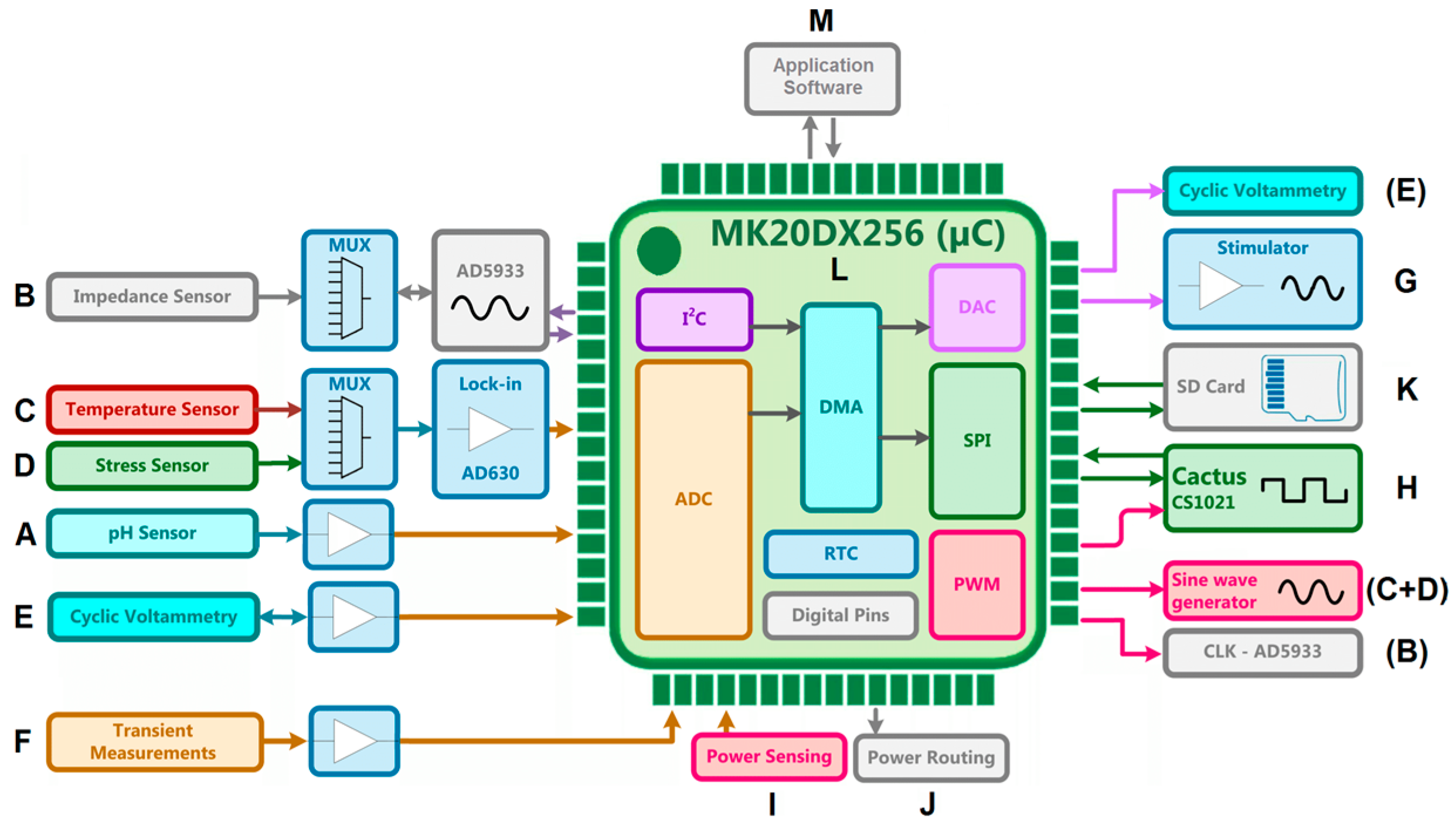
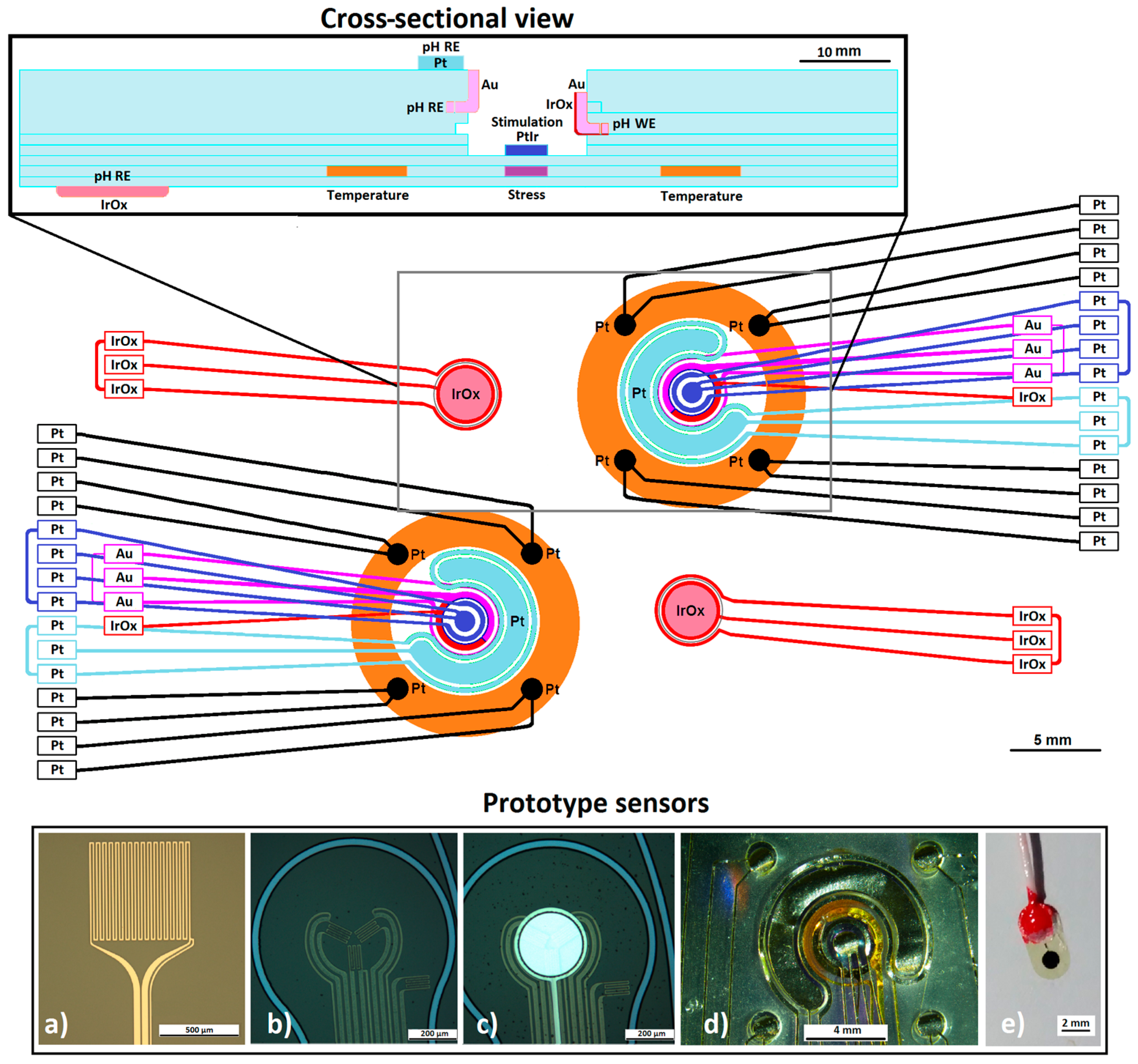
2. Materials and Methods
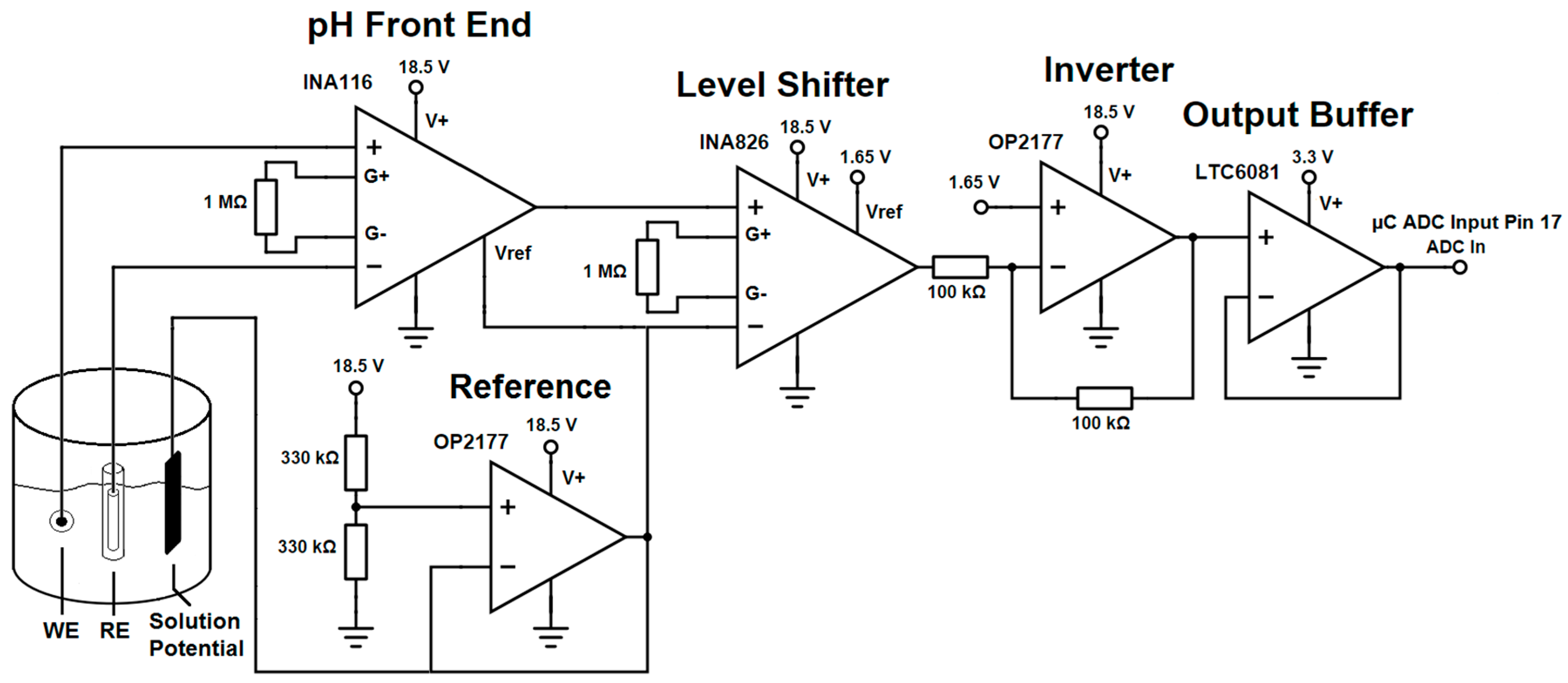
2.1. pH Measurement
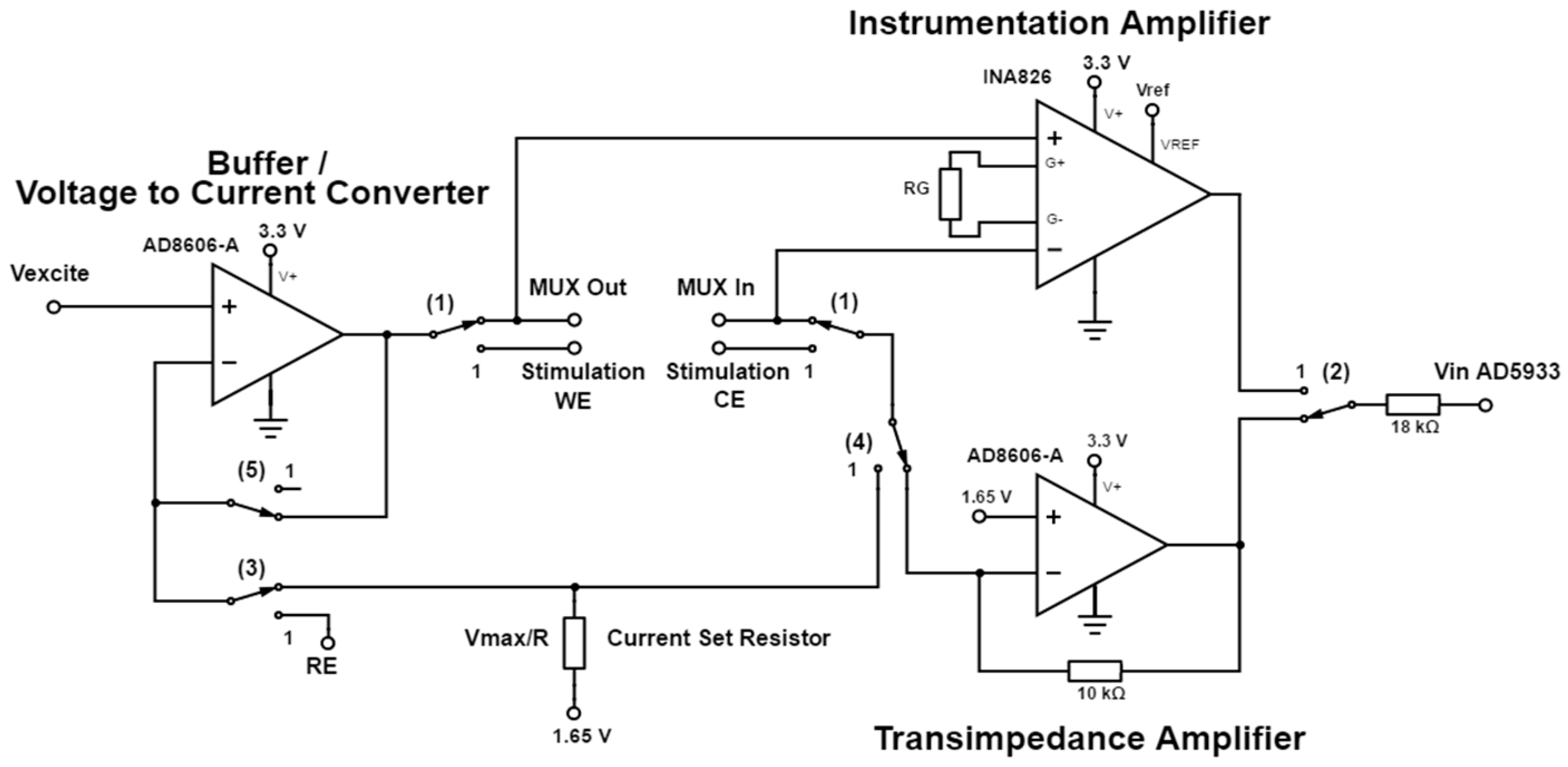
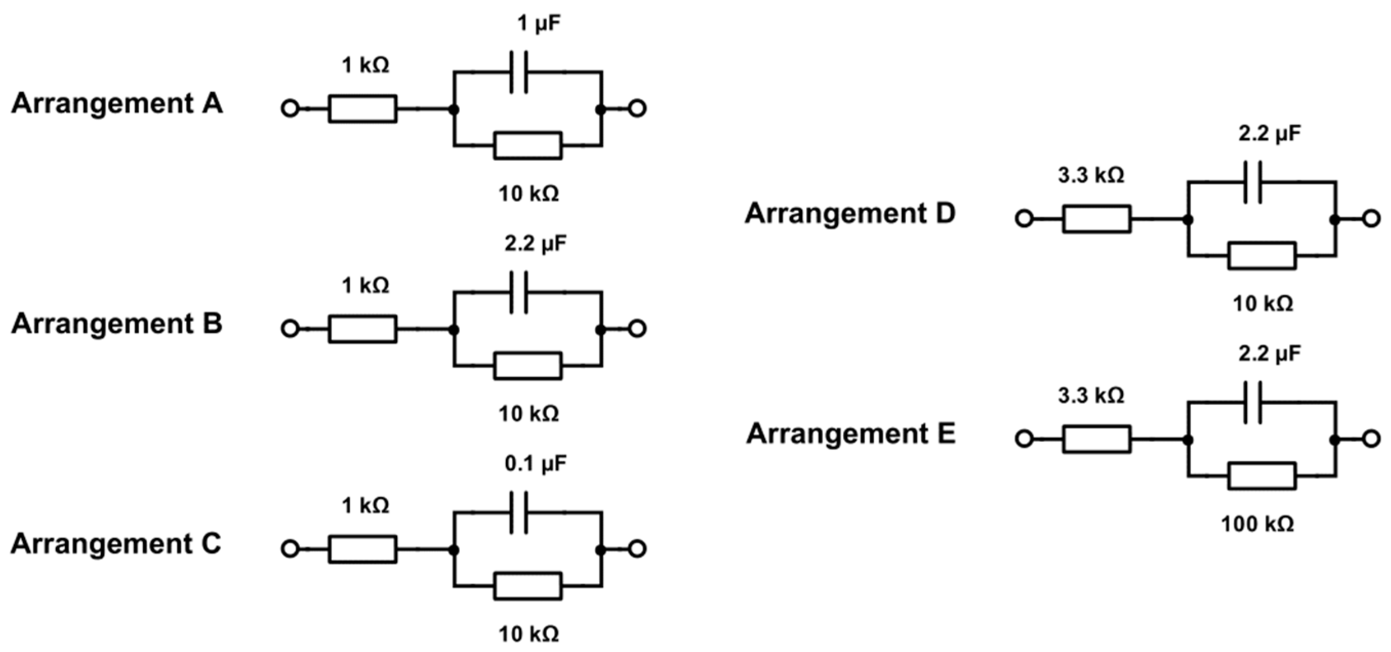
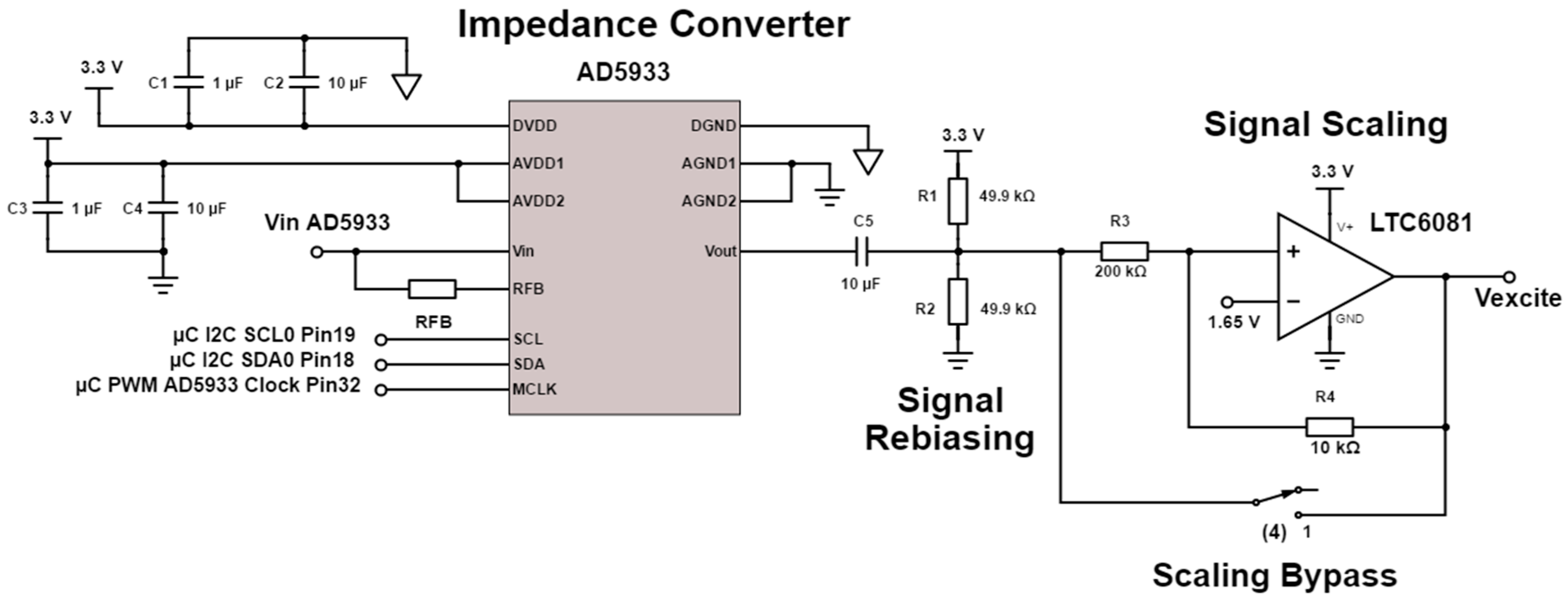
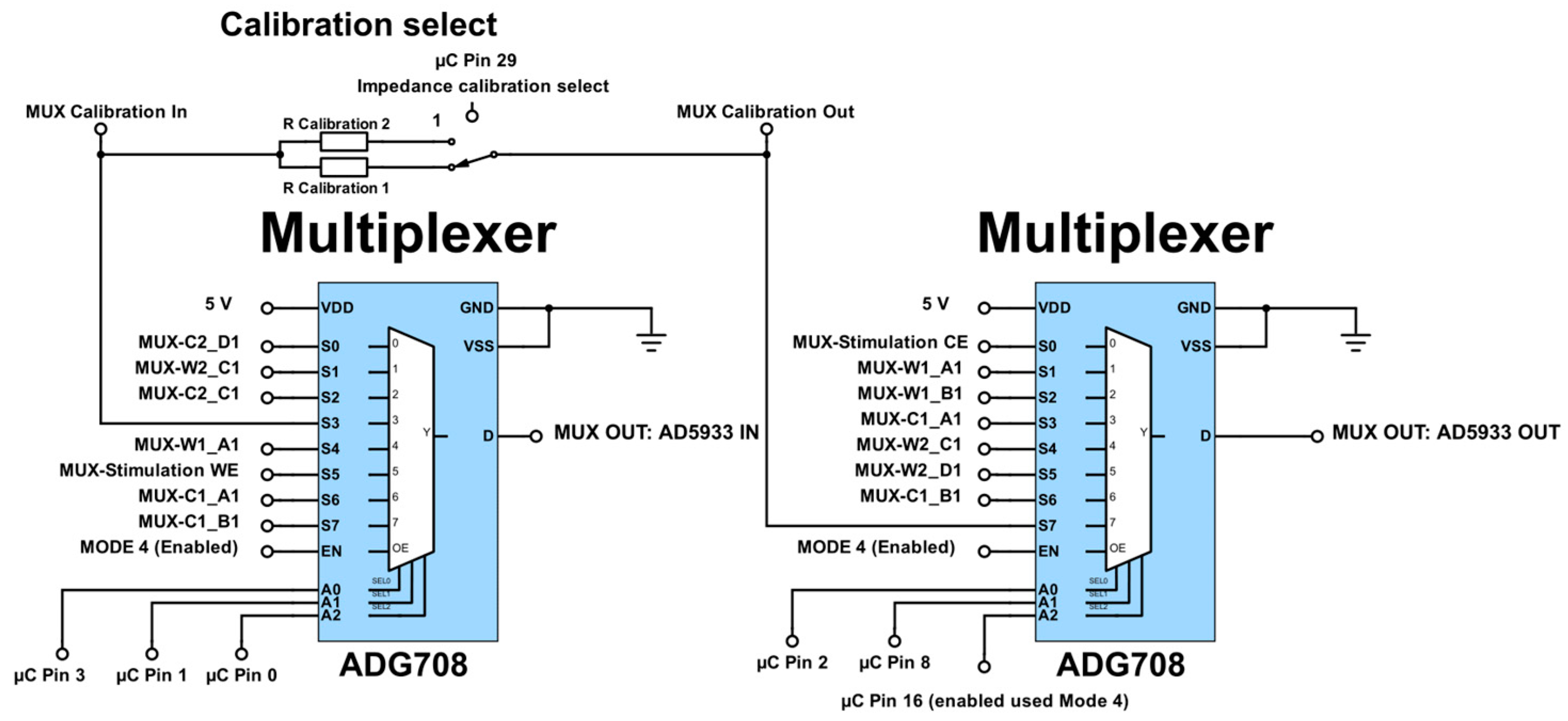
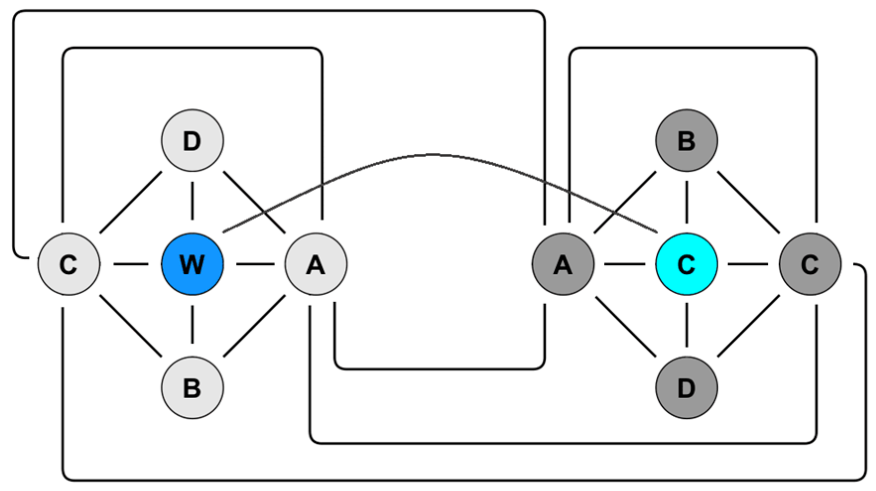
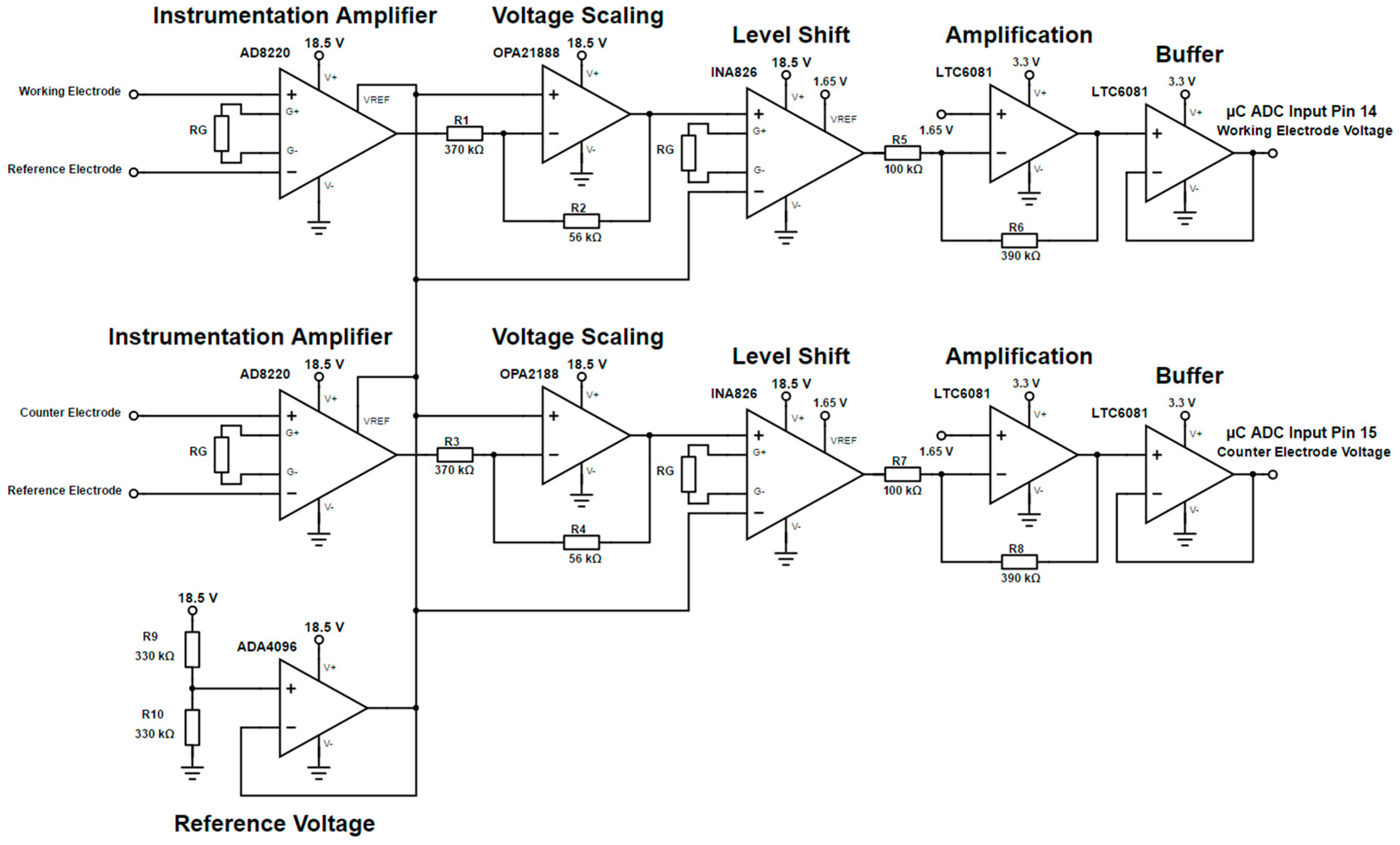
2.2. Impedance Spectroscopy
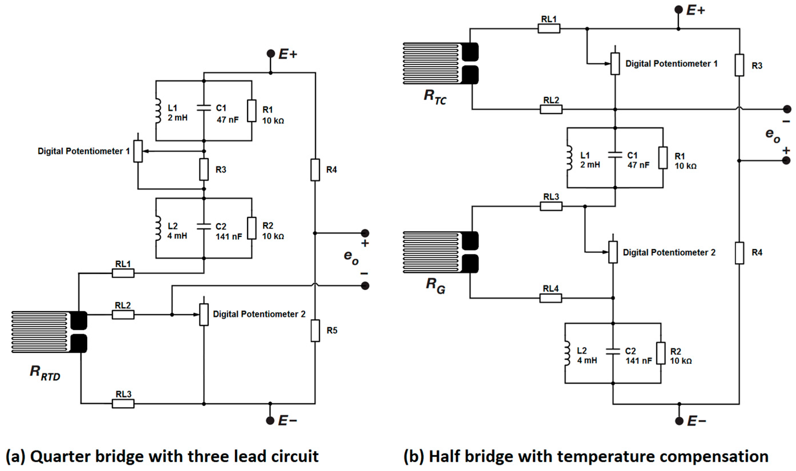
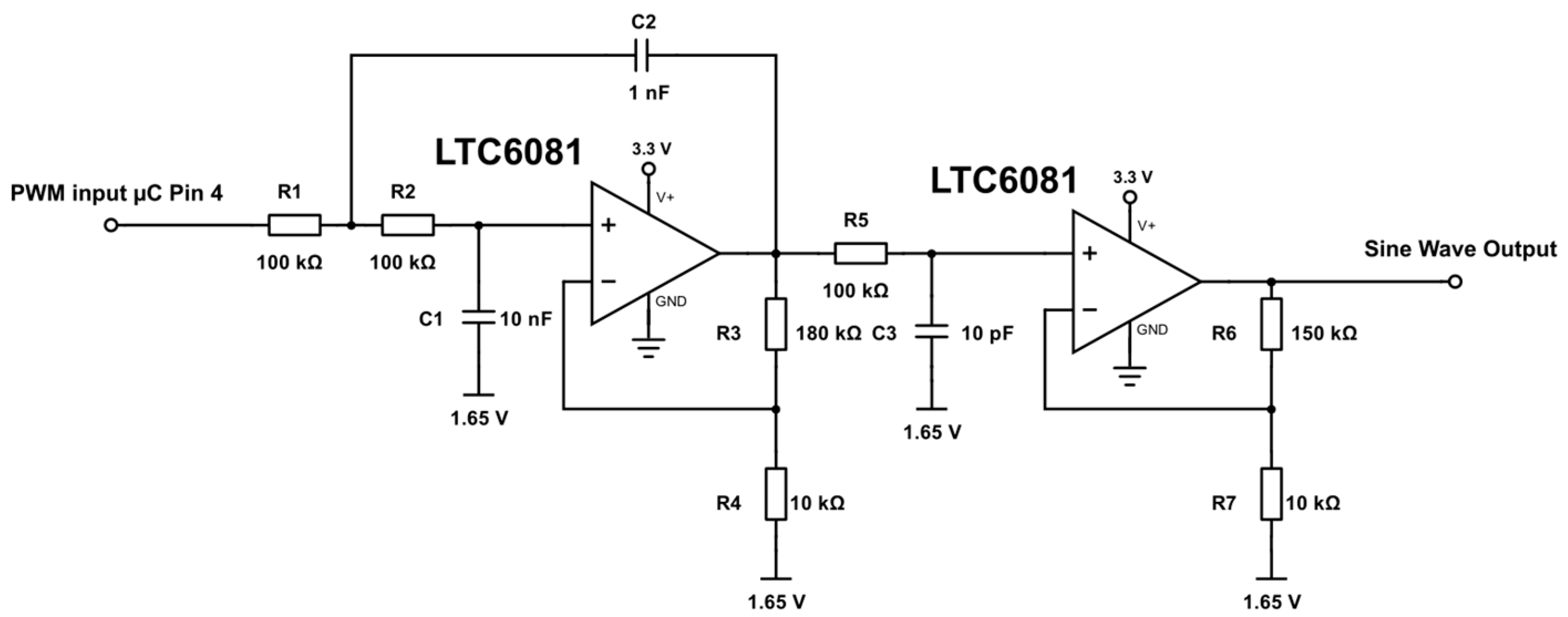
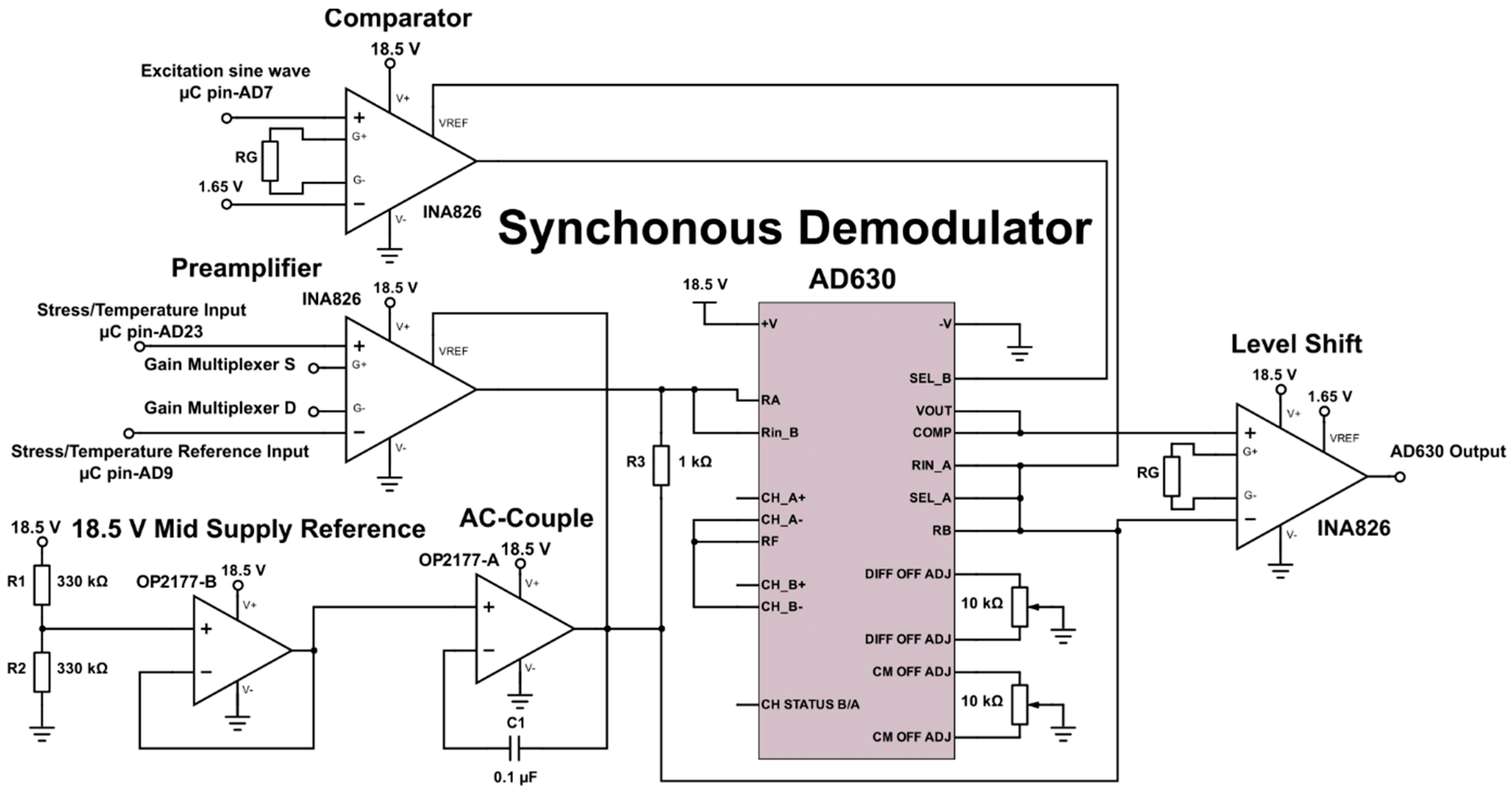
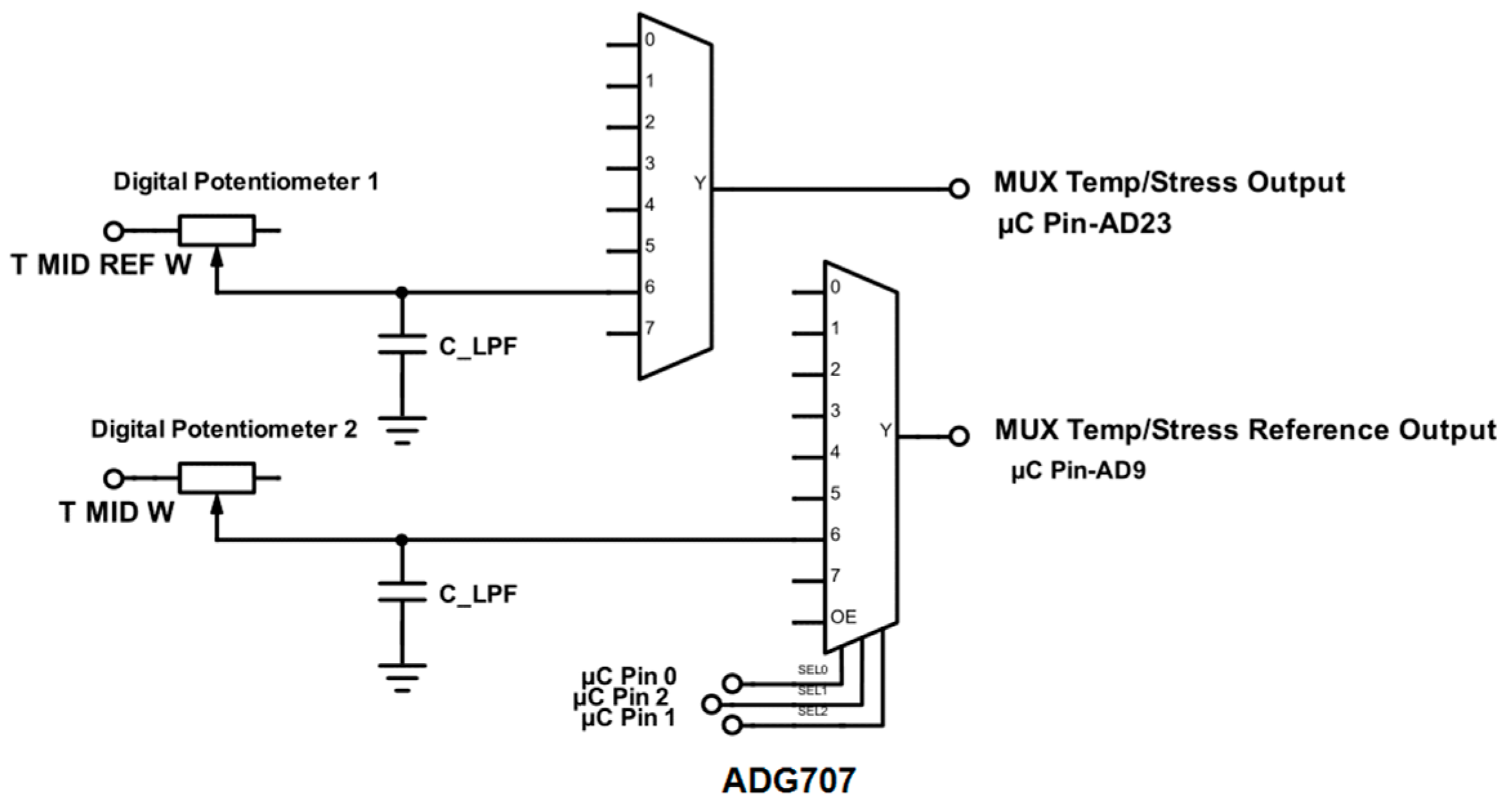
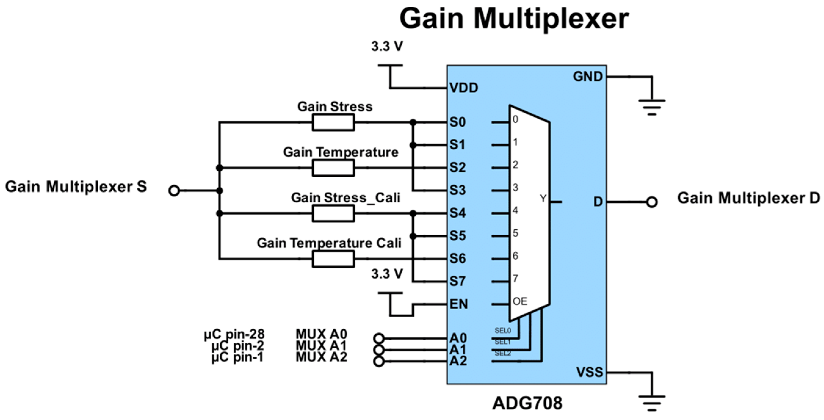
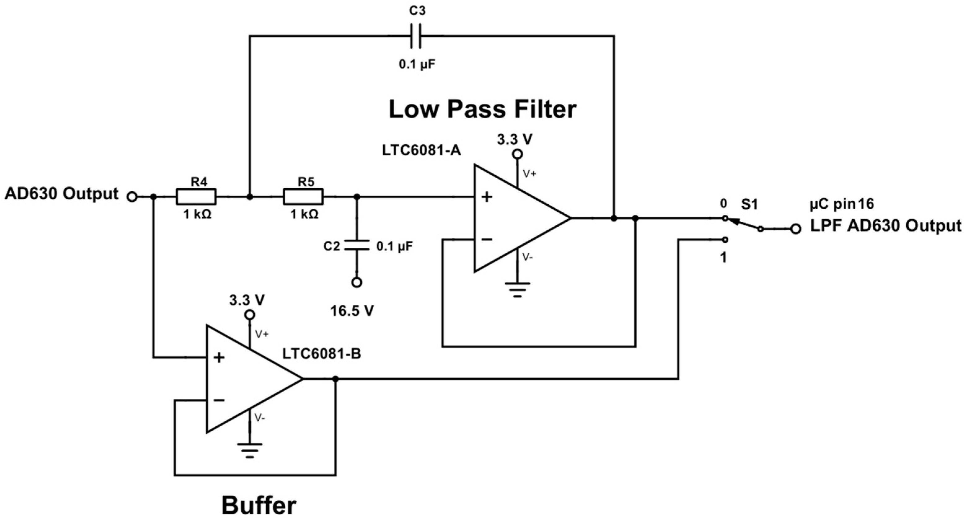
2.3. Stress/Temperature
- The changes in resistance are very small (<1 Ω) and the signal is partially or completely hidden in noise.
- The lock-in feature of the amplifier allows stimulation induced interference from the proximity to the stimulation electrodes to be filtered out.
- Being able to measure a signal with a high signal to noise ratio, allows the lock-in amplifier design to measure physical sensors in a noisy in vivo environment, where movement artefacts and electrical interference (such as those from cardiac activity) are expected.
- Potentially lengthy lead wires passing through a fluid medium could also lead to considerable interference and noise, which can be filtered out using the lock-in amplifier design.
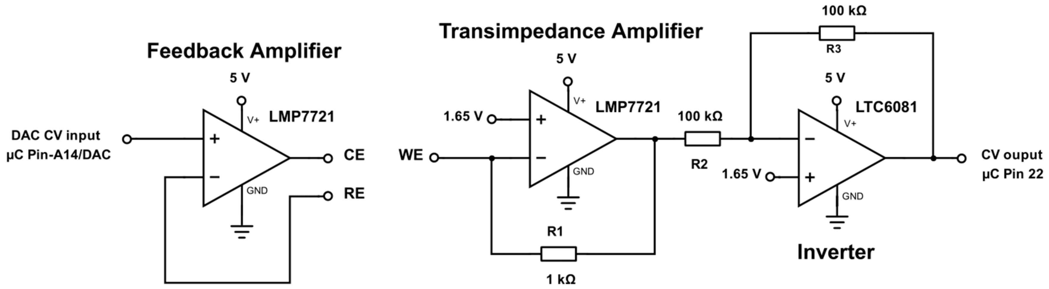
2.4. Cyclic Voltammetry
2.5. Voltage Transient Measurements
2.6. Power Consumption
3. Results
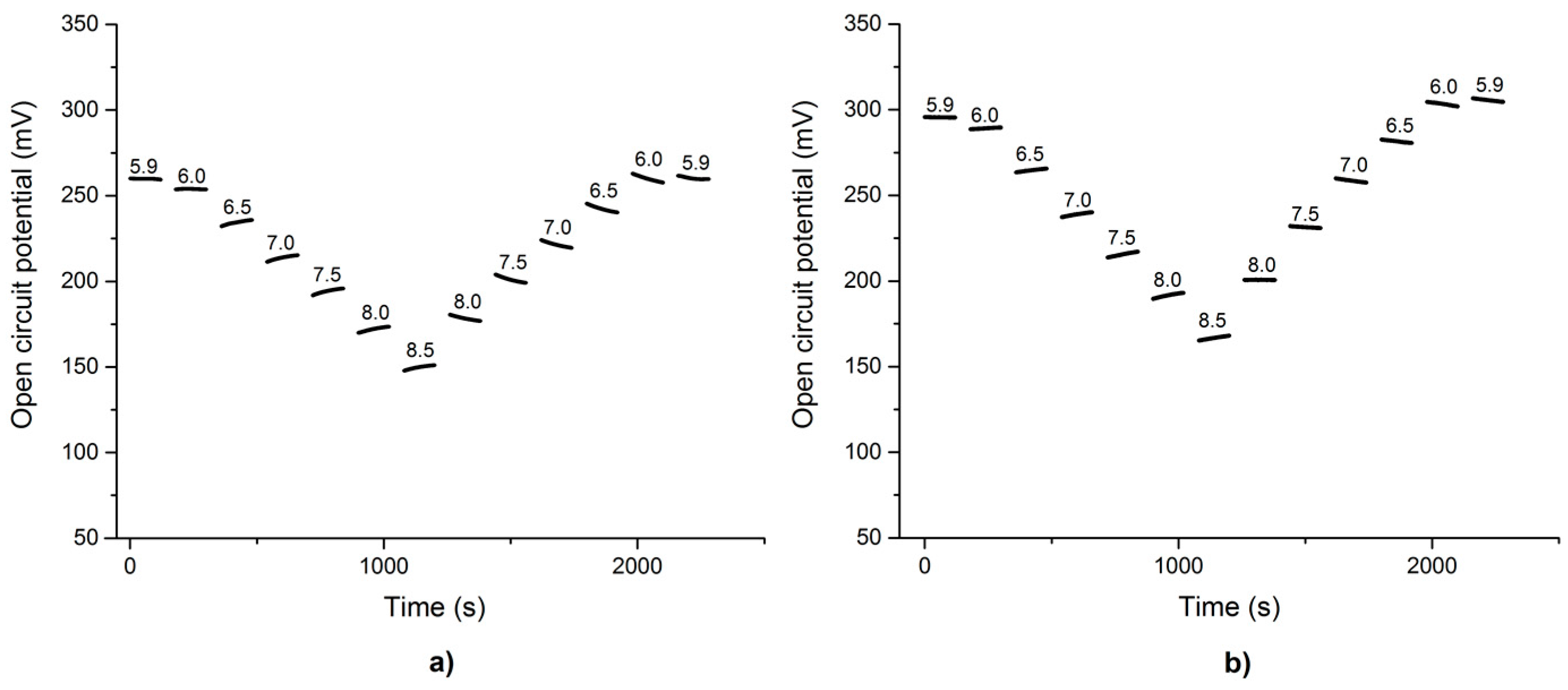
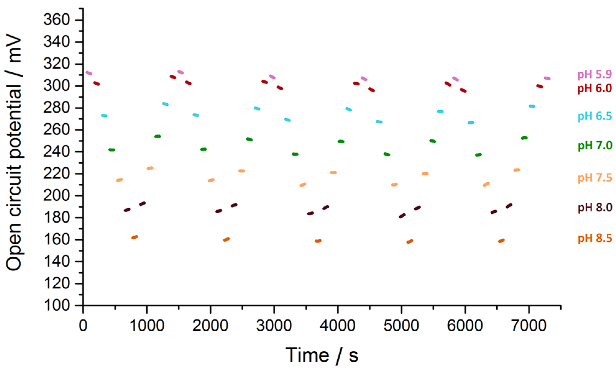
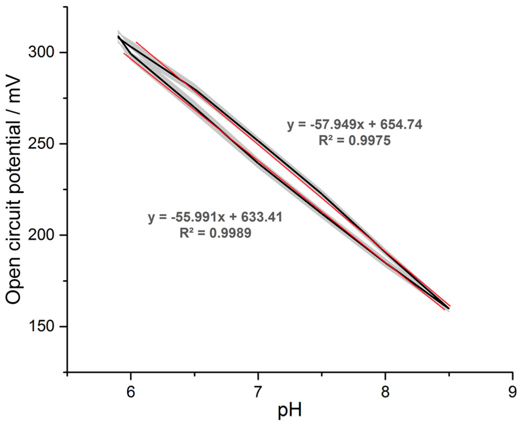
3.1. pH Measurements
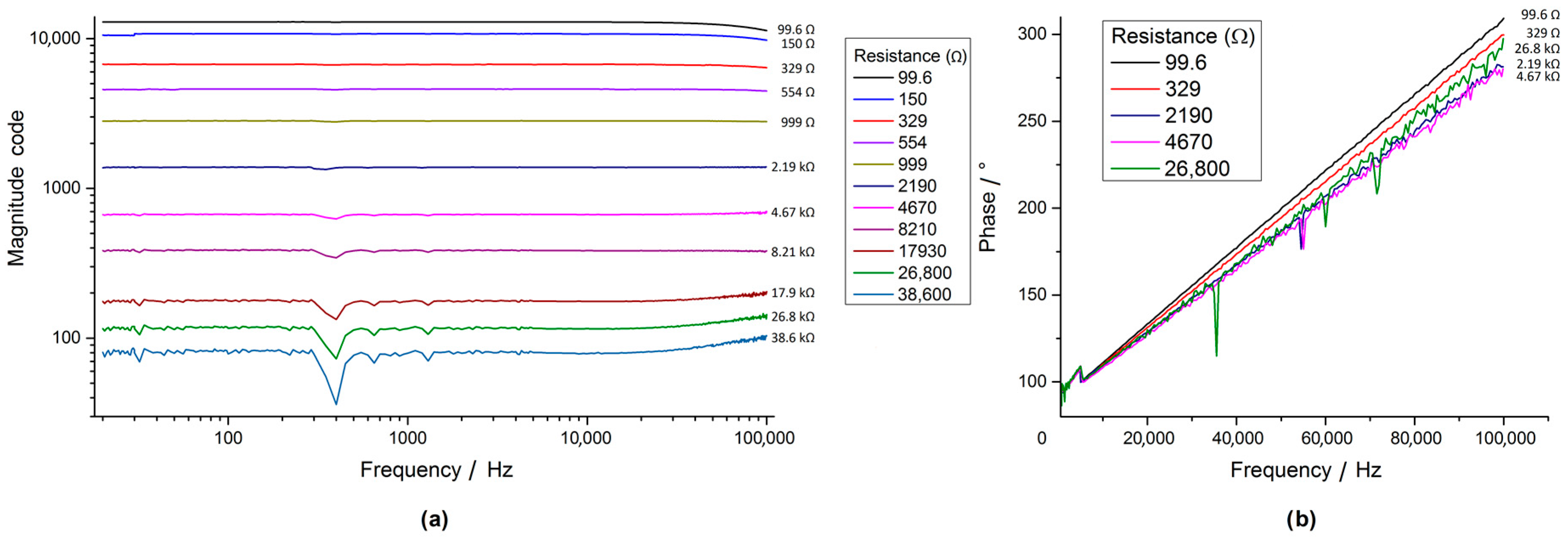
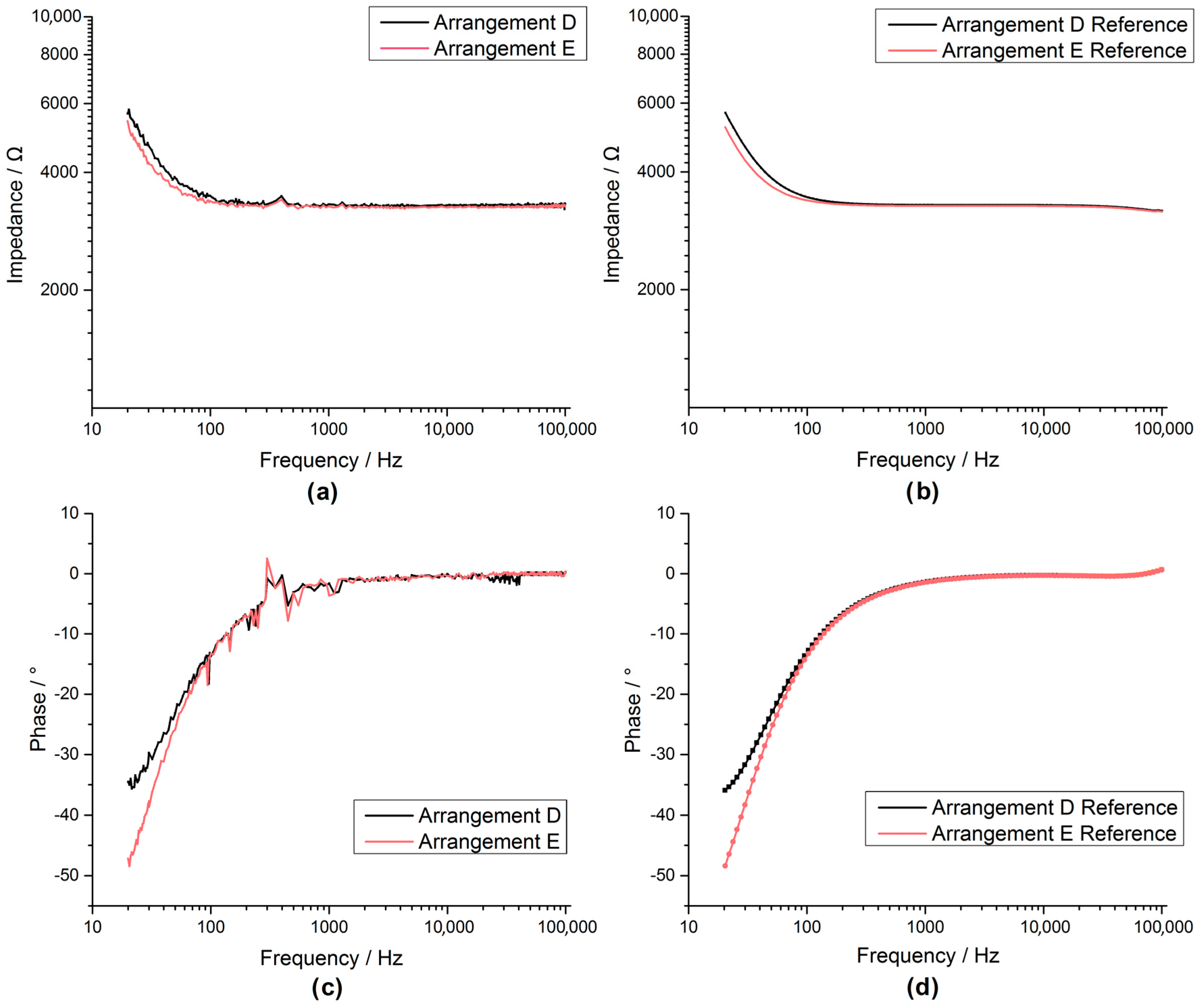
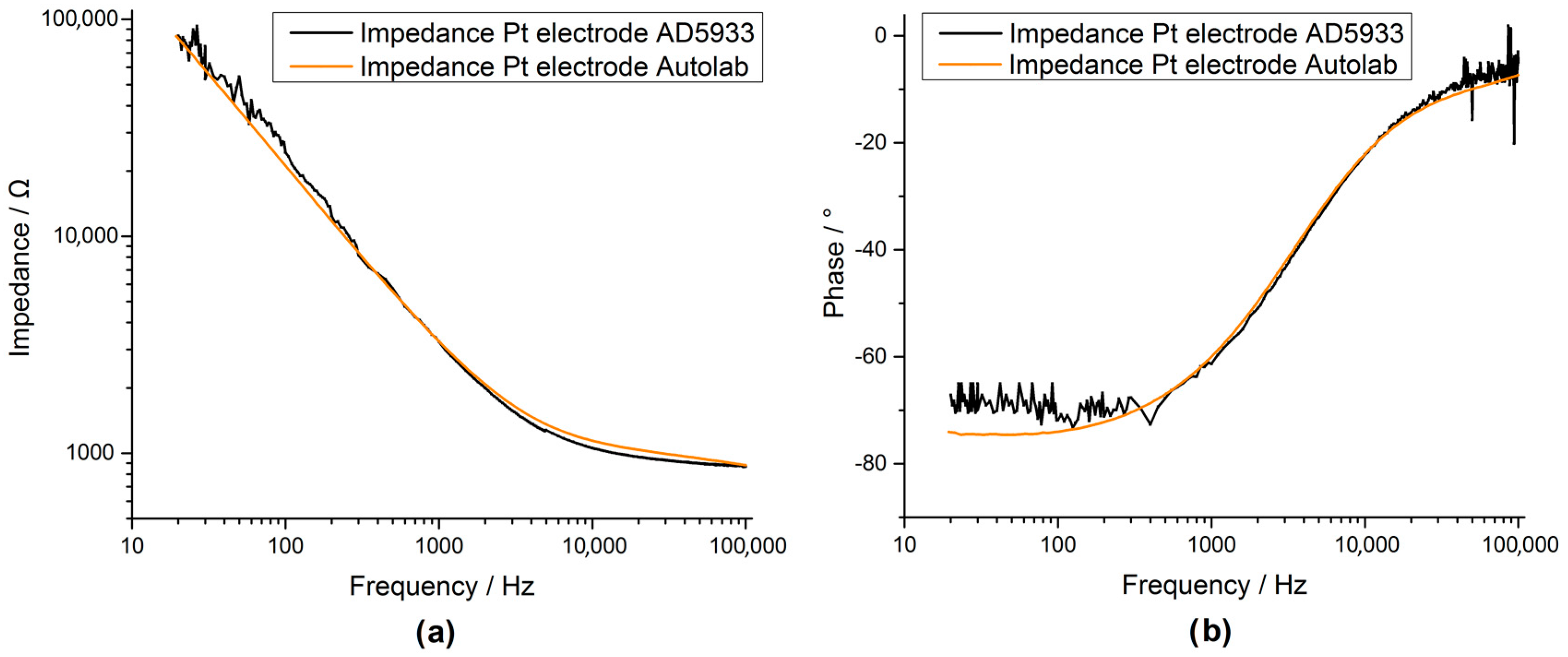
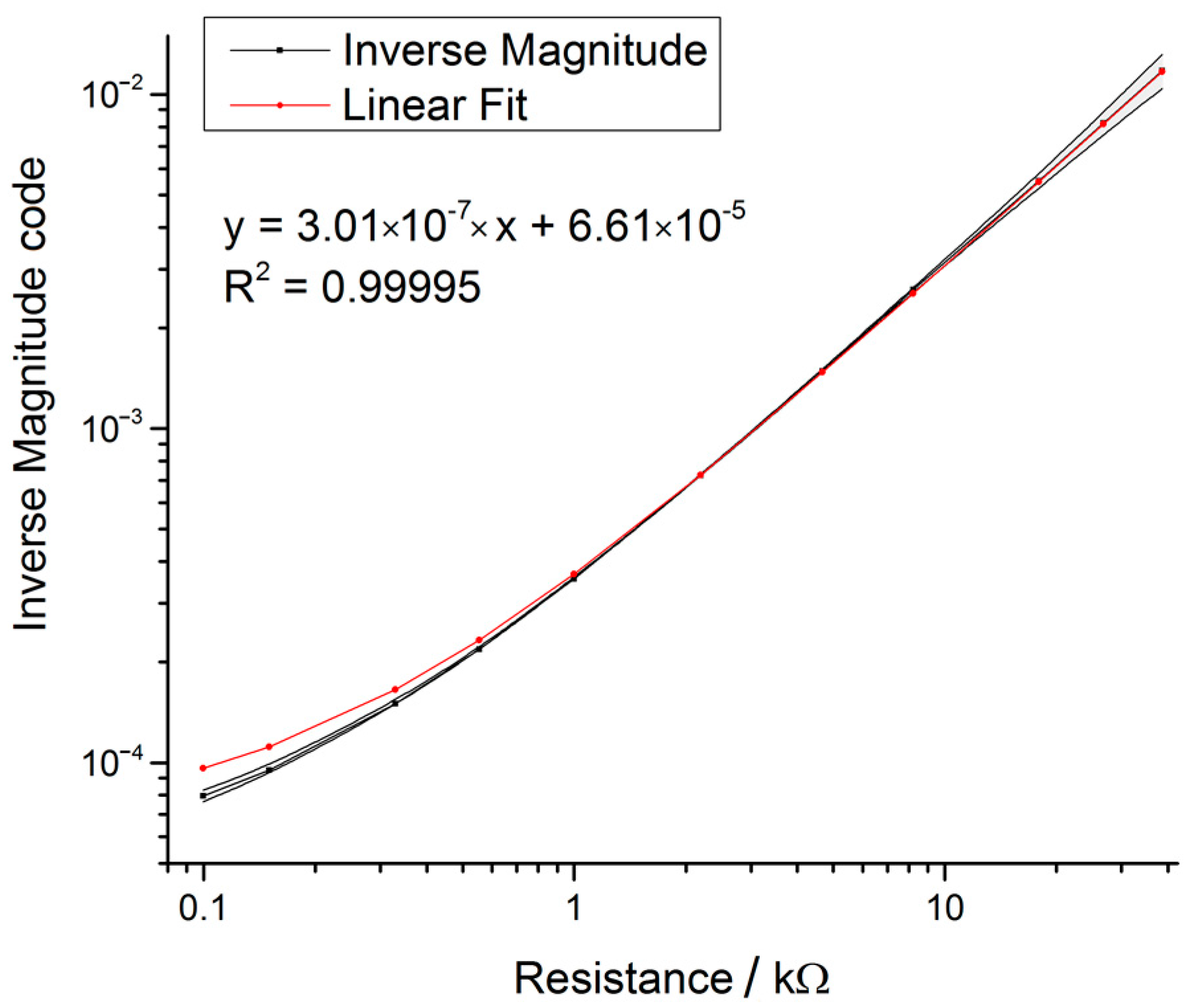
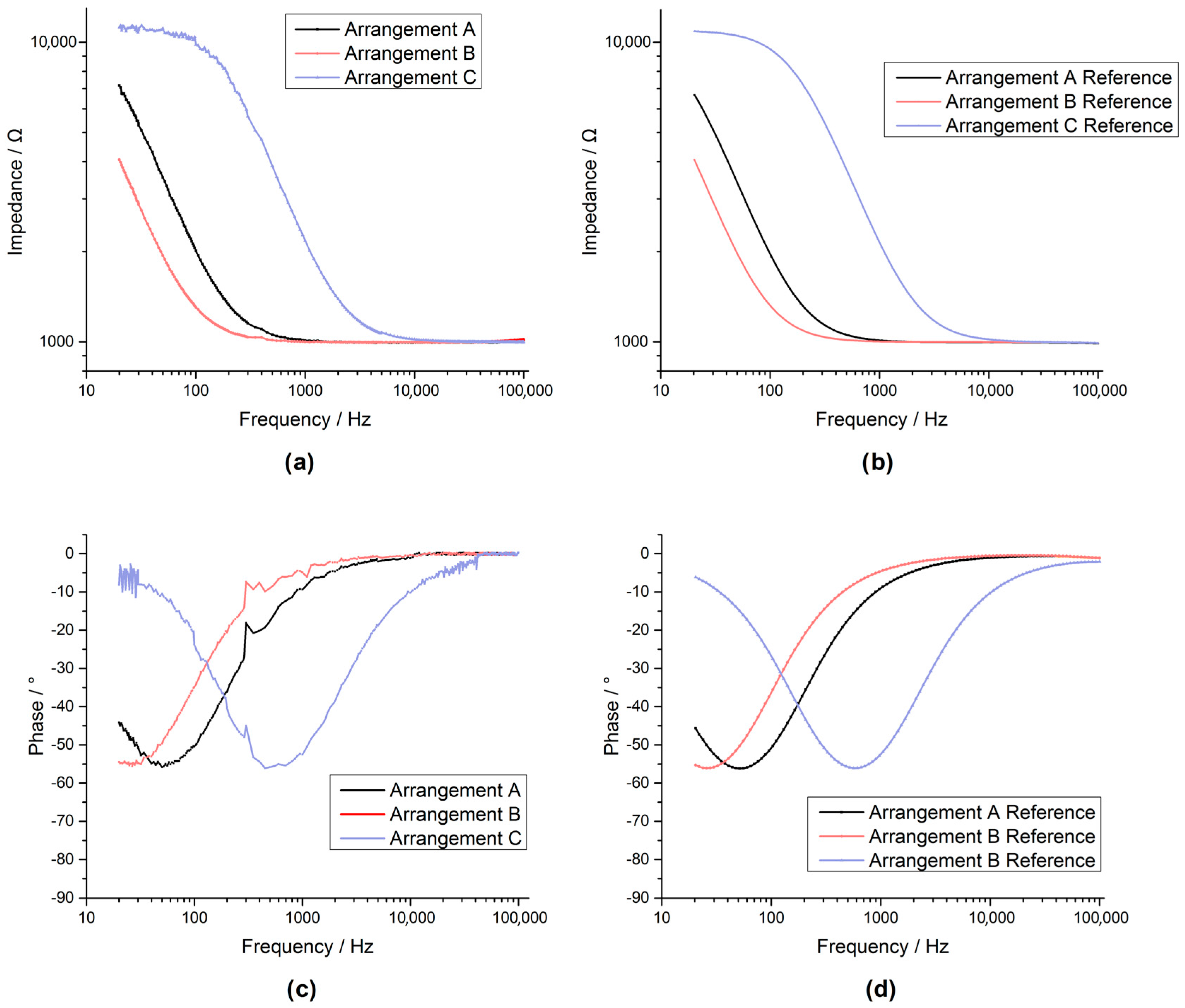
3.2. Impedance Spectroscopy
3.3. Temperature / Stress
3.4. Power Consumption
4. Discussion and Conclusions
Acknowledgments
Author Contributions
Conflicts of Interest
Abbreviations
| ADC | Analog-to-Digital Converter |
| WE | Working Electrode |
| CE | Counter Electrode |
| RE | Reference Electrode |
| CV | Cyclic Voltammetry |
| Ag | Silver |
| Cl | Chloride |
| Pt | Platinum |
| Ir | Iridium |
References
- Howlader, M.M.R.; Doyle, T.E.; Mohtashami, S.; Kish, J.R. Charge transfer and stability of implantable electrodes on flexible substrate. Sens. Actuators B Chem. 2013, 178, 132–139. [Google Scholar] [CrossRef]
- Merrill, D.R.; Bikson, M.; Jefferys, J.G.R. Electrical stimulation of excitable tissue: Design of efficacious and safe protocols. J. Neurosci. Methods 2005, 141, 171–198. [Google Scholar] [CrossRef] [PubMed]
- Cogan, S.F. Neural stimulation and recording electrodes. Annu. Rev. Biomed. Eng. 2008, 10, 275–309. [Google Scholar] [CrossRef] [PubMed]
- Mailley, S.; Hyland, M.; Mailley, P.; McLaughlin, J.A.; McAdams, E.T. Thin film platinum cuff electrodes for neurostimulation: In vitro approach of safe neurostimulation parameters. Bioelectrochemistry 2004, 63, 359–364. [Google Scholar] [CrossRef] [PubMed]
- Hu, Z.; Troyk, P.R.; Brawn, T.P.; Margoliash, D.; Cogan, S.F. In vitro and in vivo charge capacity of AIROF microelectrodes. In Proceedings of the IEEE 28th Annual International Conference of the IEEE Engineering in Medicine and Biology Society (EMBS’06), New York, NY, USA, 31 August–3 September 2006; pp. 886–889.
- Green, R.A.; Matteucci, P.B.; Dodds, C.W.D.; Palmer, J.; Dueck, W.F.; Hassarati, R.T.; Byrnes-Preston, P.J.; Lovell, N.H.; Suaning, G.J. Laser patterning of platinum electrodes for safe neurostimulation. J. Neural Eng. 2014, 11, 056017. [Google Scholar] [CrossRef] [PubMed]
- Ghoreishizadeh, S.S.; Carrara, S.; De Micheli, G. A configurable IC to contol, readout, and calibrate an array of biosensors. In Proceedings of the European Conference on Circuit Theory and Design (ECCTD), Dresden, Germany, 8–12 September 2013; pp. 1–4.
- Liao, Y.-T.; Yao, H.; Lingley, A.; Parviz, B.; Otis, B.P. A 3µ CMOS glucose sensor for wireless contact-lens tear glucose monitoring. IEEE J. Solid-State Circuits 2012, 47, 335–344. [Google Scholar] [CrossRef]
- Lu, L.; Yan, G.; Zhao, K.; Xu, F. An implantable telemetry platform system with ASIC for in vivo monitoring of gastrointestinal physiological information. IEEE Sens. J. 2015, 15, 3524–3534. [Google Scholar] [CrossRef]
- Stett, A.; Al, E. SMART implant: Electronic implants for diagnosis and monitoring. In Proceedings of the 2014 7th GMM-Workshop Energy Self-Sufficient Sensors, Magdeburg, Germany, 24–25 February 2014.
- Cavallini, A.; Baj-Rossi, C.; Ghoreishizadeh, S.; De Micheli, G.; Carrara, S. Design, fabrication, and test of a sensor array for perspective biosensing in chronic pathologies. In Proceedings of the IEEE Biomedical Circuits and Systems Conference (BioCAS), Hsinchu, Taiwan, 28–30 November 2012; pp. 124–127.
- Croce, R.A.; Vaddiraju, S.; Legassey, A.; Zhu, K.; Islam, S.K.; Papadimitrakopoulos, F.; Jain, F.C. A highly miniaturized low-power CMOS-based pH monitoring platform. IEEE Sens. J. 2015, 15, 895–901. [Google Scholar] [CrossRef]
- Ativanichayaphong, T.; Tang, S.-J.; Hsu, L.-C.; Huang, W.-D.; Seo, Y.-S.; Tibbals, H.F.; Spechler, S.; Chiao, J.-C. An implantable batteryless wireless impedance sensor for gastroesophageal reflux diagnosis. In Proceedings of the IEEE MTT-S International Microwave Symposium, Anaheim, CA, USA, 23–28 May 2010; pp. 608–611.
- Lehmann, M.; Baumann, W. New insights into the nanometer-scaled cell-surface interspace by cell-sensor measurements. Exp. Cell Res. 2005, 305, 374–382. [Google Scholar] [CrossRef] [PubMed]
- Ordonez, J.S.; Rudmann, L.; Cvancara, P.; Bentler, C.; Stieglitz, T. Mechanical deformation of thin film platinum under electrical stimulation. In Proceedings of the 37th Annual International Conference of the IEEE Engineering in Medicine and Biology Society (EMBC), Milano, Italy, 25–29 August 2015; pp. 1045–1048.
- Seo, M. Piezoelectric Response to Surface Stress Change of Platinum Electrode. J. Electrochem. Soc. 1986, 133, 1138. [Google Scholar] [CrossRef]
- Cruz, M.F.P.; Fiedler, E.; Monjarás, O.F.C.; Stieglitz, T. Integration of temperature sensors in polyimide-based thin-film electrode arrays. Curr. Dir. Biomed. Eng. 2015, 1, 529–533. [Google Scholar] [CrossRef]
- Schuettler, M.; Stiess, S.; King, B.V.; Suaning, G.J. Fabrication of implantable microelectrode arrays by laser cutting of silicone rubber and platinum foil. J. Neural Eng. 2005, 2, S121-8. [Google Scholar] [CrossRef] [PubMed]
- Porto Cruz, M.F. Integration of Temperature Sensors in Polyimide-Based Thin-Film Electrode-Arrays. Master‘s Thesis, University of Freiburg, Freiburg, Germany, 2014. [Google Scholar]
- De Sousa, M.J. Strain Gauges for the Mechanical Characterization of Implantable Microelectrodes. Master‘s Thesis, University of Freiburg, Freiburg, Germany, 2015. [Google Scholar]
- Ultra Low Input Bias Current Instrumentation Amplifier, INA116, Burr Brown. 1995. Available online: http://www.ti.com/lit/ds/symlink/ina116.pdf (accessed on 18 March 2015).
- Ng, S.R.; Al, E. An iridium oxide microelectrode for monitoring acute local pH changes of endothelial cells. Analyst 2015, 140, 4224–4231. [Google Scholar] [CrossRef] [PubMed]
- Ges, I.A.; Ivanov, B.L.; Werdich, A.A.; Baudenbacher, F.J. Differential pH measurements of metabolic cellular activity in nl culture volumes using microfabricated iridium oxide electrodes. Biosens. Bioelectron. 2007, 22, 1303–1310. [Google Scholar] [CrossRef] [PubMed]
- 1 MSPS, 12-Bit Impedance Converter, Network Analyzer, AD5933, Rev. E, Analog Devices. Available online: http://www.analog.com/media/en/technical-documentation/data-sheets/AD5933.pdf (accessed on 20 April 2015).
- Evaluation Board User Guide UG-364, Rev. 0, Anlog Devices. Available online: http://www.analog.com/media/en/technical-documentation/evaluation-documentation/UG-364.pdf (accessed on 28 April 2015).
- Horowitz, P.; Hill, W. The Art of Electronics, 3rd ed.; Cambridge University Press: Cambridge, UK, 2015. [Google Scholar]
- Balanced Modulator/Demodulator, AD630, Rev. F, Analog Devices. Available online: http://www.analog.com/media/en/technical-documentation/data-sheets/AD630.pdf (accessed on 15 May 2015).
- Stieglitz, T. Electrode materials for recording and stimulation. In Neuroprosthetics Theory Pract; Series Bioeng. Biomed. Eng. Vol. 2; Horch, K.W., Dhillon, G.S., Eds.; World Scientific: Singapore, 2004; pp. 482–511. [Google Scholar]
- Ordonez, J.S.; Boehler, C.; Schuettler, M.; Stieglitz, T. Improved polyimide thin-film electrodes for neural implants. In Proceedings of the Annual International Conference of the IEEE Engineering in Medicine and Biology Society, San Diego, CA, USA, 28 August–1 September 2012; pp. 5134–5137.
- Ordonez, J.; Schuettler, M.; Boehler, C.; Boretius, T.; Stieglitz, T. Thin films and microelectrode arrays for neuroprosthetics. MRS Bull. 2012, 37, 590–598. [Google Scholar] [CrossRef]


| Clock Frequency | Frequency Range |
|---|---|
| 16 MHz | 5–100 kHz |
| 4 MHz | 1–5 kHz |
| 2 MHz | 300 Hz–1 kHz |
| 1 MHz | 200–300 Hz |
| 250 kHz | 100–200 Hz |
| 100 kHz | 30–100 Hz |
| 50 kHz | 20–30 Hz |
| Voltage Mode | Output Excitation Voltage Amplitude | Output DC Bias Level |
|---|---|---|
| 1 | 1.98 V p-p | 1.48 V |
| 2 | 0.97 V p-p | 0.76 V |
| 3 | 383 mV p-p | 0.31 V |
| 4 | 198 mV p-p | 0.173 V |
| Source | Voltage | Current | ||
|---|---|---|---|---|
| Electrode Configuration | 2 | 3 | 2 | 4 |
| Switch (1) | 0 | 0 | 0 | 1 |
| Switch (2) | 0 | 0 | 1 | 1 |
| Switch (3) | 0 | 1 | 0 | 0 |
| Switch (4) | 0 | 0 | 1 | 1 |
| Switch (5) | 0 | 1 | 1 | 1 |
| Parameter | Resistance/Ω | |||||||
|---|---|---|---|---|---|---|---|---|
| 995.1 | 1483 | 2698 | 3892 | 5602 | 6769 | 8251 | 9772 | |
| Precision (RSD %) | 0.144 | 0.283 | 0.865 | 1.29 | 1.826 | 1.638 | 2.607 | 2.810 |
| Trueness error (%) | −0.456 | −0.03 | −0.274 | 0.172 | −0.250 | 0.299 | −0.121 | −0.138 |
| Module | Power Consumption/mW |
|---|---|
| pH (Single) | 58.0 |
| Impedance | 48.9 |
| Stress/Temperature | 119.0 |
| Cyclic Voltammetry | 41.1 |
| Transient Measurements | 72.4 |
© 2016 by the authors; licensee MDPI, Basel, Switzerland. This article is an open access article distributed under the terms and conditions of the Creative Commons Attribution (CC-BY) license (http://creativecommons.org/licenses/by/4.0/).
Share and Cite
Rieger, S.B.; Pfau, J.; Stieglitz, T.; Asplund, M.; Ordonez, J.S. Concept and Development of an Electronic Framework Intended for Electrode and Surrounding Environment Characterization In Vivo. Sensors 2017, 17, 59. https://doi.org/10.3390/s17010059
Rieger SB, Pfau J, Stieglitz T, Asplund M, Ordonez JS. Concept and Development of an Electronic Framework Intended for Electrode and Surrounding Environment Characterization In Vivo. Sensors. 2017; 17(1):59. https://doi.org/10.3390/s17010059
Chicago/Turabian StyleRieger, Stefan B., Jennifer Pfau, Thomas Stieglitz, Maria Asplund, and Juan S. Ordonez. 2017. "Concept and Development of an Electronic Framework Intended for Electrode and Surrounding Environment Characterization In Vivo" Sensors 17, no. 1: 59. https://doi.org/10.3390/s17010059
APA StyleRieger, S. B., Pfau, J., Stieglitz, T., Asplund, M., & Ordonez, J. S. (2017). Concept and Development of an Electronic Framework Intended for Electrode and Surrounding Environment Characterization In Vivo. Sensors, 17(1), 59. https://doi.org/10.3390/s17010059