1. Introduction
Magnetic sensors have been used extensively in different fields like vehicle detection systems and biosensing applications [
1,
2,
3,
4]. A variety of magnetic sensors for sensing moderate or lower magnetic fields at low cost are available viz. split-drain magnetic field effect transistor (MAGFET), Hall plate, etc. The physical phenomenon of carrier deflection of moving charges by the application of magnetic field in the inversion layer of the MOSFET has been exploited initially in [
5,
6,
7]. The applied magnetic field perpendicular to the inversion layer can be sensed by an imbalance of currents or the Hall voltage depending on the design of the sensing device. This approach does not interfere the electrical characteristic of the MOSFET, as reported in [
6]. This kind of sensors can be batch-fabricated at very low cost and is able to detect the low magnetic field at room temperature.
As an another alternative to using the MOSFET inversion layer as the active area for magnetic field sensing applications, the drain of the traditional MOSFET can be equally divided into two or three parts [
8,
9,
10,
11,
12,
13,
14]. These drains share equal amounts of current under no influence of the magnetic fields. In the presence of the magnetic field across the inversion layer of the split-drain MOSFET (MAGFET), an imbalance in current can be detected between these split-drains, as the created Lorentz force deflect carriers in the channel and this current imbalance is proportional to the applied magnetic field. From [
12] it can be noted that the current imbalance is related to the deflection parameters including channel length, mobility of the charged carriers, and the magnetic field strength. Although, to get the equal currents in two drains the design of the sensor must be very accurate geometrically, otherwise a large amount of offset current will degrade the sensor performance. To overcome this offset error, complex design techniques must be implemented viz. chopping spinning technique [
15] or offset-trimmable array [
16]. Also, the MAGFET structure is prone to noise-related issues that noticeably reduce the resolution of the sensors.
In another approach, Wakiya et al. [
17] proposed drain current modification by the magnetic field, but the device in that case is a Pt/MZF/YSZ NMOS device. As reported in [
17], the device offers a small amount (order of pA) of the drain current increment due to the vertically applied magnetic field (i.e., the drain current modification) by increasing the mobility of the electrons. Simultaneously, the applied magnetic field pushes the carries away from the channel which decreases the mobility—such comments are self-contradictory.
Gabara [
18] reported the creation of a magnetic field by on-chip metal loops, however, in this work, the proper characterization of the device has been ignored, and instead limited to oscillation frequency.
Therefore, all the previous works either focused on Hall effect measurements, MAGFETs, or on the oscillation frequency measurement instead of device characterization. Therefore, the drain current modulation by the very small on-chip magnetic field for a MOSFET device with single-drain structure remains unexplored. In this paper, the detailed characterization of drain current in n-MOSFET has been carried out. The magnetic field for this work has been generated by an on-chip metal loop, which leads to a deflection of the charged carriers in the channel region and, as a result, a significant amount of drain current difference can be observed. This change in drain current ascribed to change in mobility, and the change in mobility is also calculated from the measured drain current. The change in substrate current can also be observed and is shown in the following sections. The change in drain current due to the applied magnetic field in n-MOSFET can lead us to the conclusion that this single-drain normal-gate n-MOSFET can be used as a potential magnetic sensor.
3. Experimental Results and Discussions
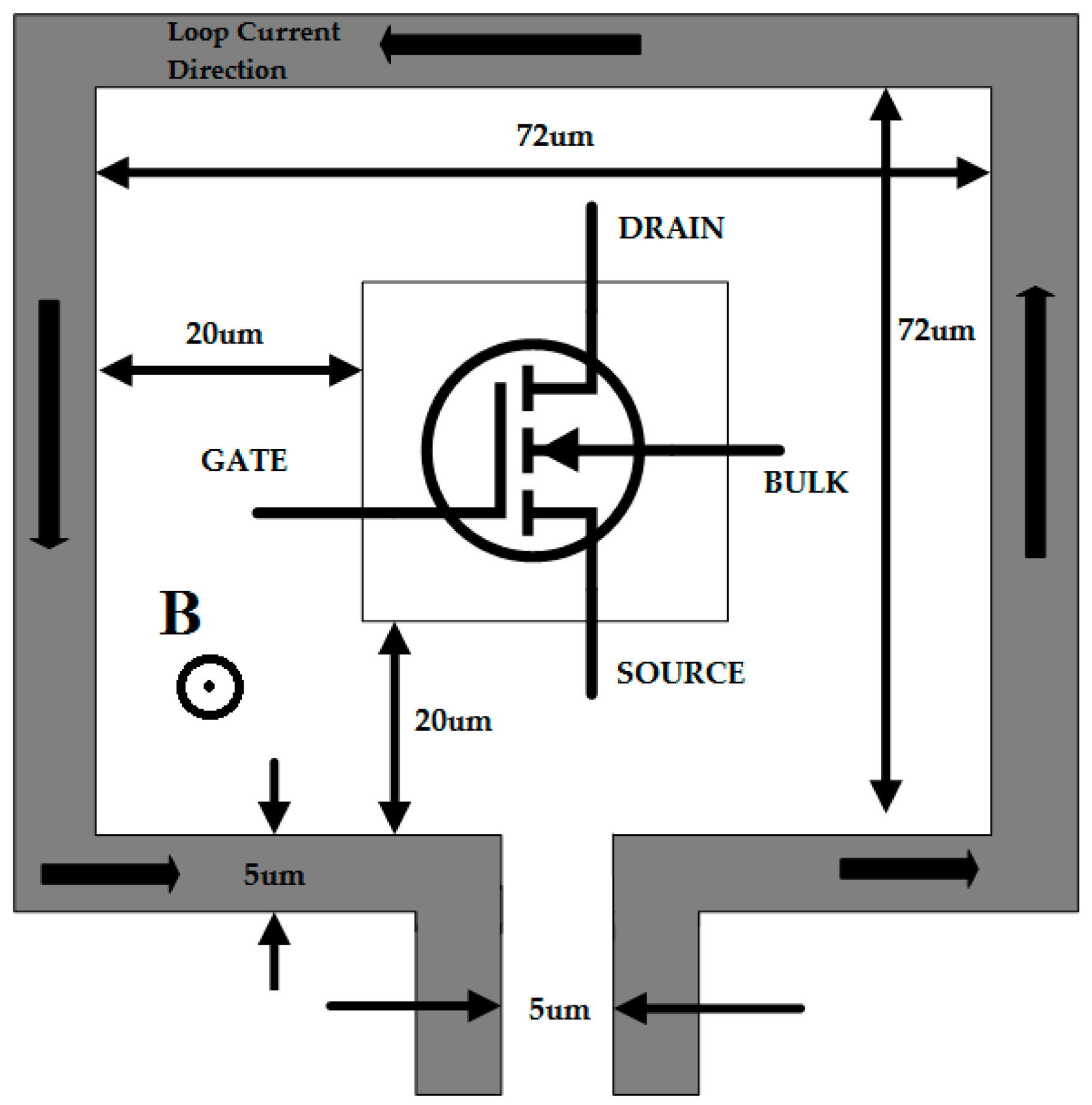
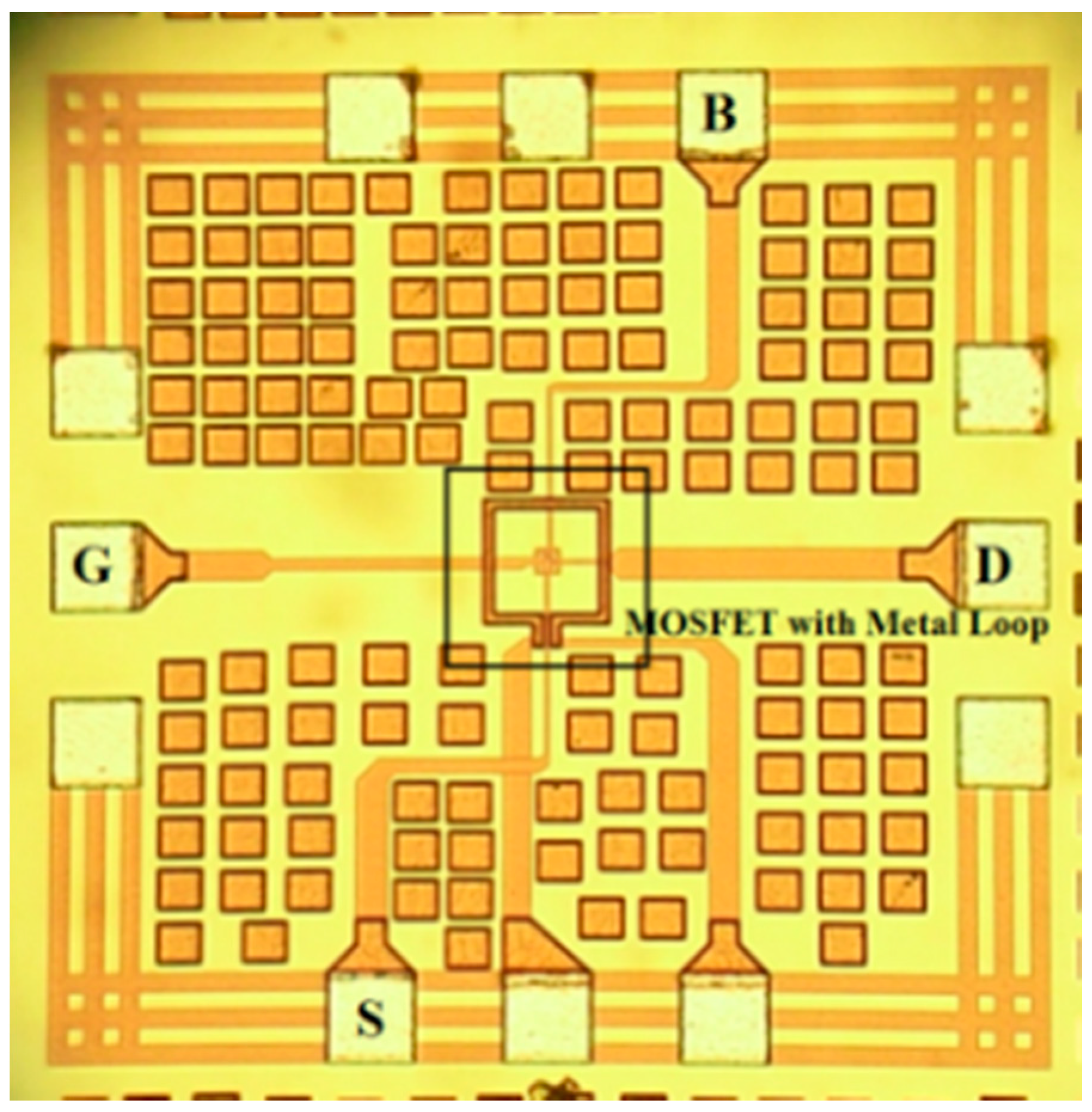
The device under test was fabricated using TSMC 0.18 µm standard CMOS process with channel length 0.18 µm and channel width 18 µm, the gate oxide thickness is about 37 Å and the gate material is polysilicon. The chip photograph is shown in
Figure 3.
A square metal loop was designed and the device was placed at the center of the loop to get the maximum effect of the created magnetic field in the active area of the device under test (DUT). The DUT is much smaller in dimension than that of the metal loop around it, and also the DUT is placed at the center of the metal loop. So the magnetic field created by the metal loop is considered to be uniform throughout the DUT. The top metal used in the MOSFET is Metal 3 whereas the loop was created using Metal 5. The distance between the metal loop and the DUT is very small. For these abovementioned reasons, the spatial variation of the magnetic field will be negligible on the DUT. On the other hand, the uniform-sized metal loop acts like a small Helmholtz coil. Therefore, the generated magnetic field is considered uniform and the direction of the magnetic field can be controlled precisely, which in turn minimizes the effect of spatial variation of the magnetic field on DUT as well.
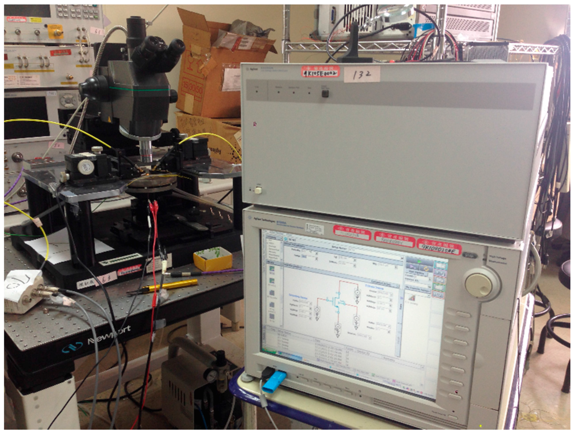
Throughout this article all the measurements were performed under direct current (DC) bias, just to ensure that a normal-gate single-drain MOS transistor can be used as a magnetic sensor. Although, as the importance of alternating current (AC) response characteristic measurements are inevitable, so it can be done as the continuation of this work. The measurements were carried out in room temperature on the anti-vibration probe station using Agilent B1500A semiconductor device parameter analyzer as shown in
Figure 4. After connecting the DUT with probes in the probe station and wire bonding, it was very hard to shield the DUT using metal, as the available probe station was not shielded. The DUT was placed on top of a surface where the effect of the magnetic field was very low and this was reconfirmed using F. W. Bell 5180 Gauss/Tesla meter so that the presence of electromagnetic interference would be very low around DUT. The gate and drain of the DUT were connected using radio frequency (RF) probes via high-precision current measurement ports of Agilent B1500A to measure the current very precisely. The source, the substrate terminals, and the metal loop were connected using wire bonding methods and via medium-range precision ports from the Agilent B1500A system. However, a proper shielding around the device might provide more accurate results.
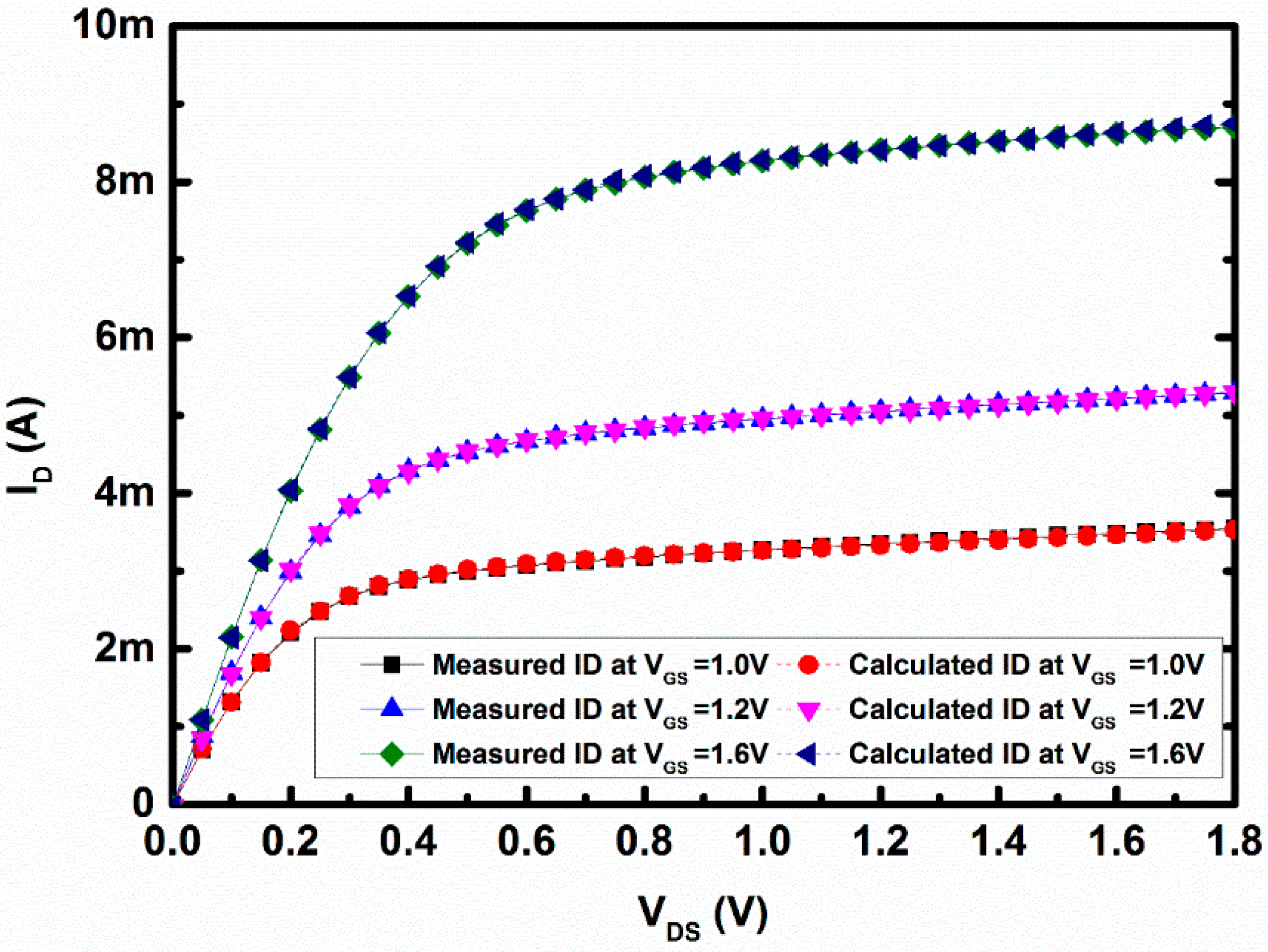
Solid lines in
Figure 5 represent the I
D–V
DS characteristic for the n-MOSFET structure without the applied magnetic field, where the vertical axis represents drain current (I
D) in Ampere (A) and the horizontal axis represents the change in drain-to-source voltage (V
DS). The gate-to-source voltages for these three sets of curve were fixed at 1.0 V, 1.2 V, and 1.6 V, respectively. The basic equations governing carrier flows in the channel of the n-MOSFET are given in Equations (3) and (4), respectively.
In the above equations, channel width (W) = 18 µm, channel length (L) = 0.18 µm, and dielectric constant ε
ox =
F/m. From I
D–V
GS plot the threshold voltage (V
t) has been extracted by curve fitting and its value was 0.32 V. Applying Equations (3) and (4) to the above values and corresponding drain currents, the mobility, oxide thickness (
m), and short-channel effect parameter lamda (λ) were calculated for each curve to reduce the error. Calculated lamda (λ = 0.0849) and mobility were used to calculate the drain current for the corresponding V
DS, which ensures nearly 2% error of the measured values. Calculated I
D–V
DS curve from the Equations (3) and (4) was shown in broken lines in
Figure 5, where (●) denotes the calculated curve for V
GS = 1 V, (▼) represents same for V
GS = 1.2 V and (◄) represents same for V
GS = 1.6 V. The data in
Figure 5 were collected without applying any magnetic field. This set of data was collected to compare whether the calculated data and the measured data were well-matched or not. The substrate current was also measured, but since the DUT was not stressed by the magnetic field, the substrate current was negligible in magnitude, as expected.
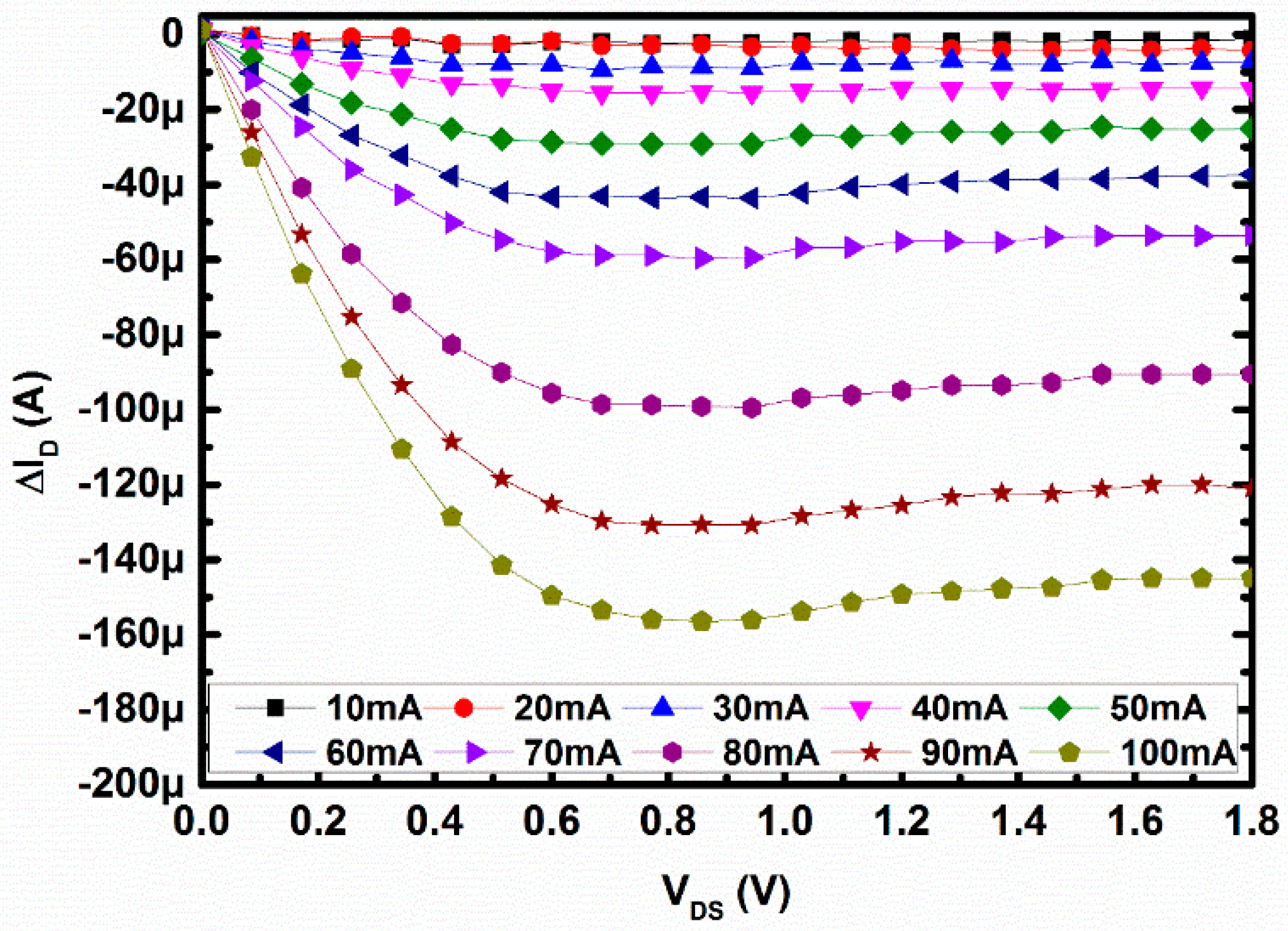
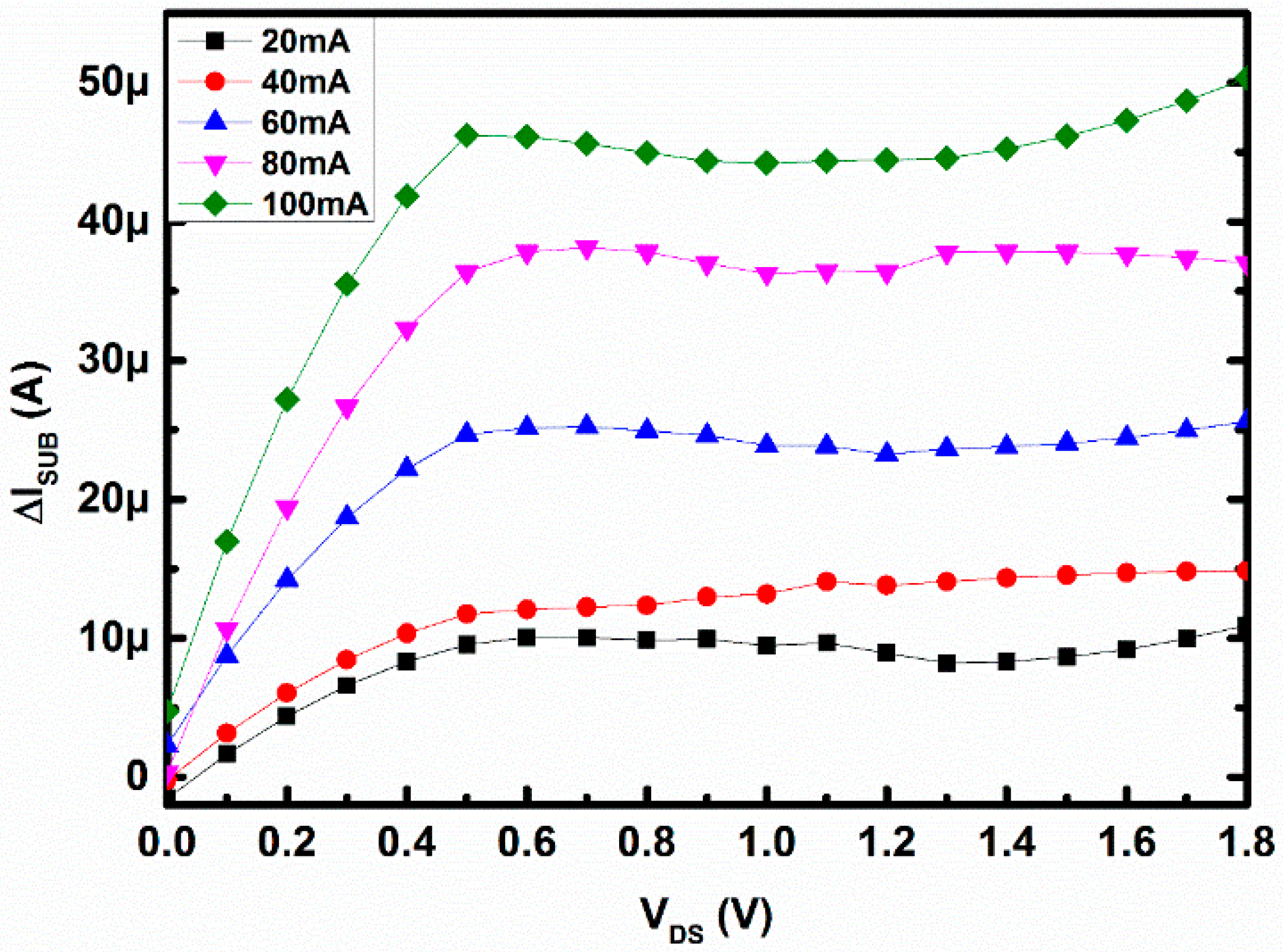
To evaluate the change in drain current due to F
B, ΔI
D has been defined as the difference between the drain currents with and without the magnetic field generated by the on-chip loop. From the aforementioned explanation in
Section 2, due to the generated magnetic field the effective drain current will decrease; this can be observed in
Figure 6. The change of drain current (ΔI
D) with respect to drain-to-source voltage (V
DS) has been displayed in
Figure 6, in which the horizontal and vertical axes refer to V
DS in V and drain current (ΔI
D) in A. Each curve refers to the difference between current due to no magnetic field and current with the applied magnetic field through the loop from 0–100 mA with the step of 10 mA. During this measurement, the gate-to-source voltage was fixed at 1 V. As seen, the current through the metal loop (i.e., F
B) was increasing the change in drain current, which was getting higher. This is because whenever F
B is getting higher, more mobile carriers are pushed away from the channel, hence the drain current is decreased, and a maximum of 145 µA or 8.06 µA/micron device width at 1.8 V V
DS, difference current can be measured. The change of drain current at V
DS = 1.8 V and V
GS = 1 V is around 4.084%. Such change in drain current can be described in terms of either the change in threshold voltage or the change in mobility of charged carriers in the channel. Since the F
B was acting horizontally to the channel, the threshold voltage of the device cannot be affected and hence the change in drain current will be ascribed due to the change in mobility of the charged carriers. From the measured I
D in the saturation region, the electron mobility variation at different magnetic fields has been derived. The carrier mobility in the channel affected by factors like mobility related to scattering of phonons, screened coulomb scattering, and mobility related to surface roughness scattering. Thus, the increase of the strength of the magnetic field affects the scattering factors effectively, which effectively decreases the mobility of the channel electrons and, as a result, the I
D decreases further.
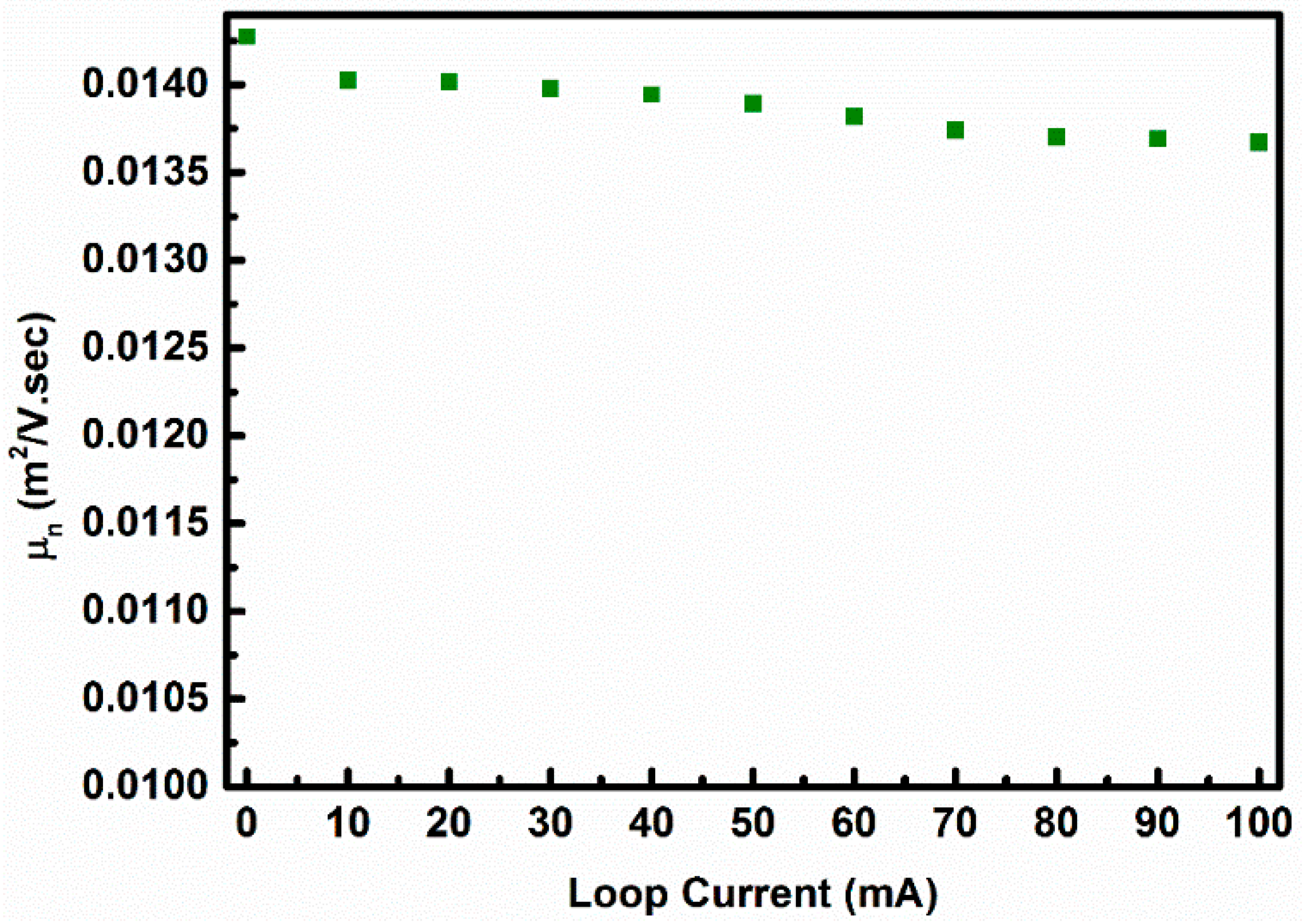
The estimated change in mobility with the change in the applied loop current is shown in
Figure 7, where the vertical axis represents the change in mobility in m
2/V·s, whereas the horizontal axis represents the applied current through the metal loop in mA. As can be seen from
Figure 7, the effective mobility is decreasing as the current through the loop is increasing, which in turn is decreasing the I
D effectively. The change in mobility is around 4.227%.
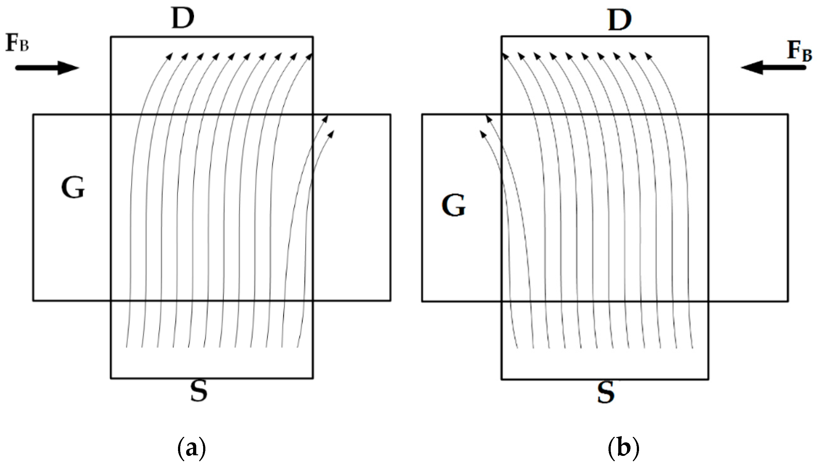
As shown in
Figure 2, due to the Lorentz force the carriers will drift away from channel towards the bulk for both directions of the force, i.e., when the loop current is reversed, electrons from the channel will still drift away towards bulk, but in a different direction as shown in
Figure 2b. So the change in mobility is expected to be the same even with the change in direction of the applied loop current. From
Figure 7 it can be deduced that the change in mobility is related to the applied loop current, or in other words, to magnetic field, which suggests that the mobility of the charged carriers might be altered by the application of the magnetic field.
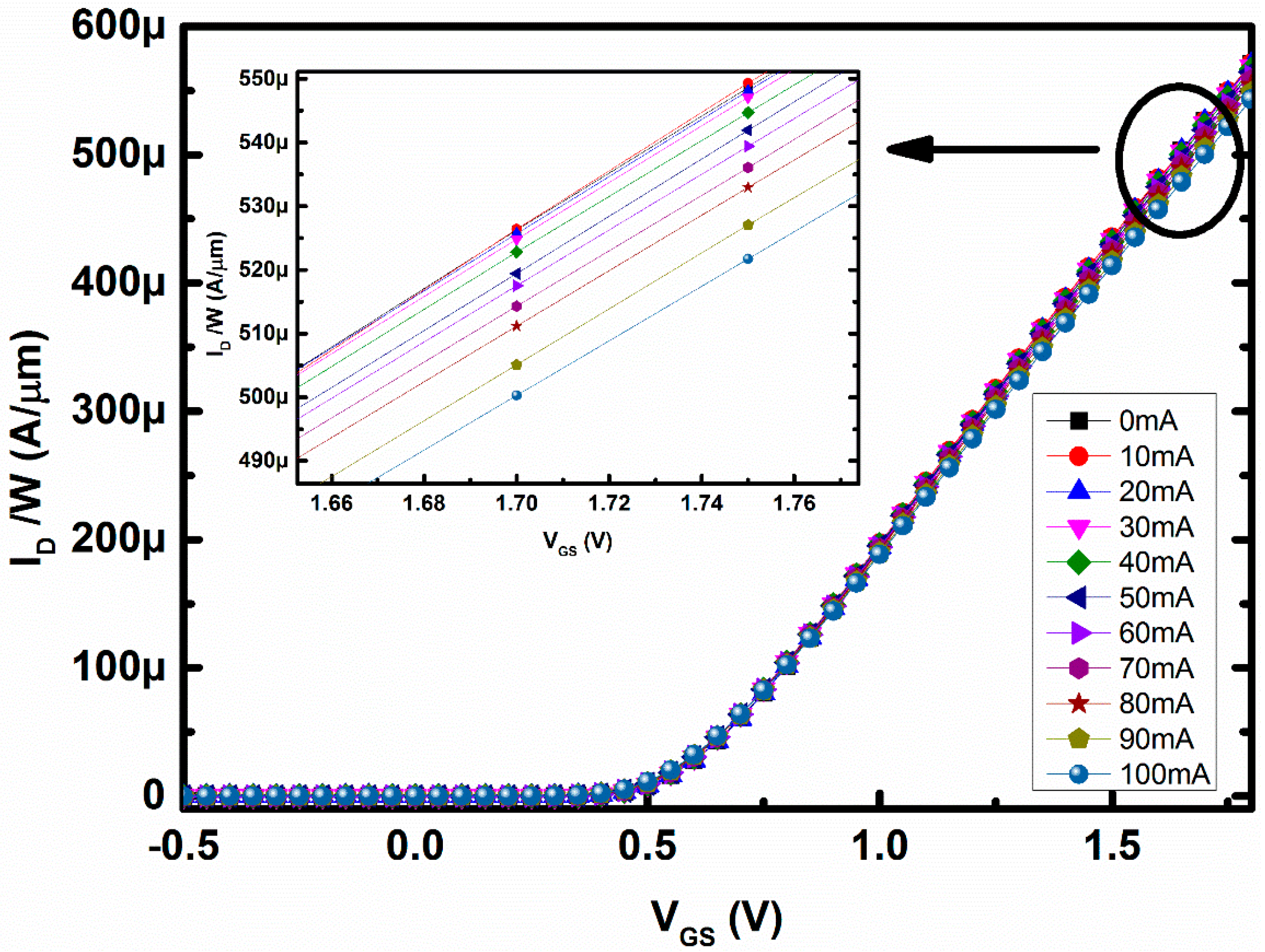
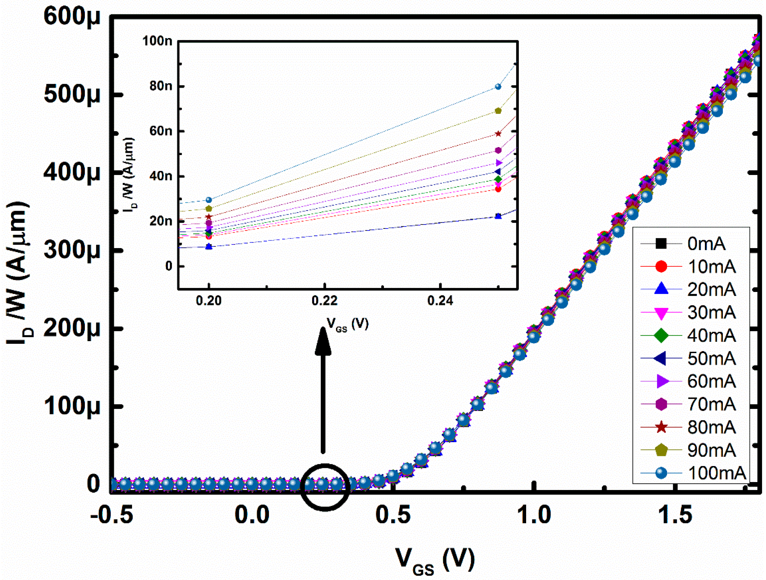
Figure 8 shows the relation between drain current per micron width (I
D/W) and gate-to-source voltage (V
GS) for different amounts of loop current through the metal loop around the MOSFET and with the V
DS fixed at 1 V. In
Figure 8, the gate-to-source voltage (V
GS) was magnified at around 1.5–1.7 V, i.e., the device was operating in the saturation region of operations. It can be seen from
Figure 8 that I
D was decreasing with increasing magnetic field. In the saturation region, drift was the dominant mechanism for the charged carriers and hence the I
D decreases due to the effect of magnetic field. However, when the device operates in the subthreshold regions the change in I
D is in the opposite direction, as shown in
Figure 9. The applied magnetic field will change the mobility in the subthreshold region, similar to the saturation region of operation. However, the Lorentz force created by the applied magnetic field will change the surface potential, and as a result the threshold voltage of the DUT in the subthreshold region will change as well [
20]. Hence, the current will increase irrespective of the decrement of mobility, as the change in threshold voltage is dominant over that of mobility change. However, due to the change in mobility in the opposite direction, the current in the subthreshold region will not be able to increase exponentially, as shown in
Figure 9.
During the data collection for
Figure 6 there was a significant amount of change in substrate current as shown in
Figure 10. From
Figure 10 it can be seen that the change in substrate current is lower in magnitude than that of the change in drain current seen in
Figure 6. This change arises due to the fact that some of the drifted electrons from the channel might have been lost. Due to recombination in the p-type substrate, the rest electrons will add up to the substrate current, which is shown in
Figure 10. As shown in
Figure 2, for any direction of the loop current, the drifted-away electrons will go towards substrate only and not towards the gate, hence there was no change in the effective gate current observed. Also, due to the thick gate oxide for 0.18 µm standard CMOS technology, the moved-out electrons will not penetrate towards the gate to build up an effective gate current. In conclusion, as the trend of the change in substrate current is opposite to that of the change in drain current, so the charge neutrality is justified in this case.
Figure 10 represents the change in substrate current with V
DS, whereas the gate voltage was fixed at 1 V as mentioned earlier. These pushed-out electrons might create higher substrate current with increasing magnetic field, as expected, where the vertical axis represents a change in substrate current and the horizontal axis represents the applied drain-to-source voltage in
Figure 10. This measurement was done with loop current 0–100 mA. Around 50.24 µA or 2.78 µA/micron device width at 1.8 V V
DS, difference substrate current has been measured.
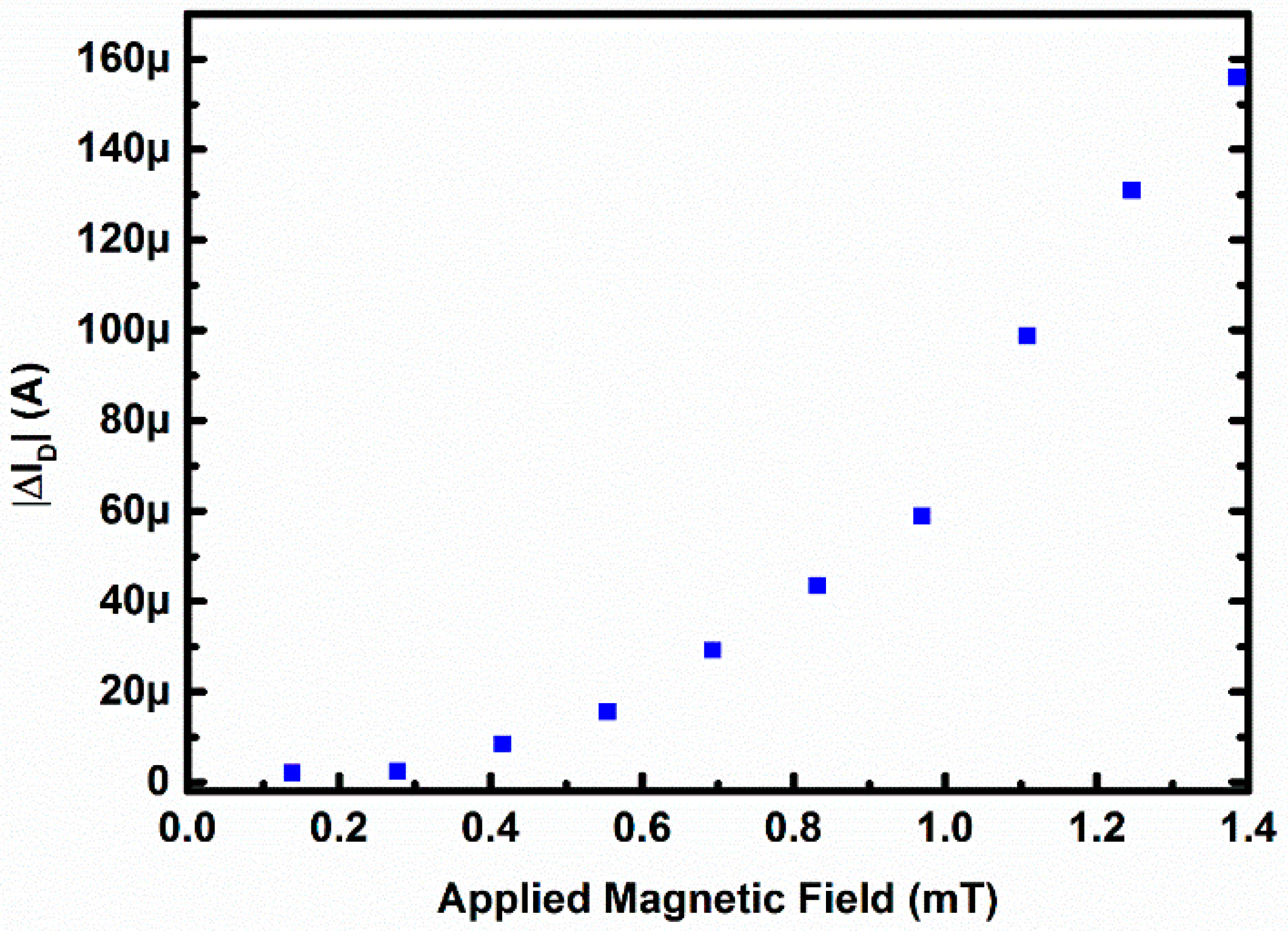
Figure 11 demonstrates that the MOSFET is directly responding to the magnetic field. The horizontal axis represents the value of the applied magnetic field, where as the vertical axis represents the absolute value of the change in drain current for V
GS = 1 V and V
DS = 0.8 V. From
Figure 11 it can be seen that the absolute change in current is proportional to that of the change in magnetic field.
Finally, the influence of magnetic field over drain current has been measured by defining the sensitivity based on the change of drain current upon the application of the magnetic flux on the charged carriers in the channel of n-MOSFET. The sensitivity can be defined as
where Δ
ID is the difference between the drain current with and without magnetic field and B is the magnetic field strength. The measured value of the generated magnetic field, using F.W.Bell 5180 Gauss/Tesla meter, was very low because the probe of the Gauss meter cannot reach below 1 cm from the chip surface due to probing and wire bonding in the chip. So, to get the value of the applied magnetic field, Equation (2) was used and the calculated value was 1.385 mT. Using the value of the magnetic field, the sensitivity has been calculated and it was about 4.084% (29.6 T
−1) at V
DS = 1.8 V and V
GS = 1 V and 3.68% (26.57 T
−1) at V
DS = 0.25 V and V
GS = 1 V.
A comparison table (
Table 1) is provided to compare this work with previously reported works. In this performance comparison the proposed idea has been compared in the view of sensitivity, channel length, strength of applied magnetic field, device type, etc. For this work, TSMC 0.18 µm standard CMOS technology was used to fabricate the DUT. The dimension of the device is much smaller than that of the metal loop area and also the DUT is placed at the center of the loop. The metal loop is made up of Metal 5, i.e., the distance of the metal loop is very small from that of the DUT. So the created magnetic field is considered to be uniform, and the magnetic field is expected to be uniform throughout the DUT due to its small size. So, to compute the magnetic field strength the method was used as proposed in [
19]. This was a rectangular-shaped normal MOSFET with normal gate and single drain. The maximum applied magnetic field was 1.385 mT. The estimated sensitivity was 4.084% or 29.6 T
−1, which suggests that the proposed structure was not only very effective but also more sensitive with respect to the proposed work. As reported in [
12], the sensitivity was related to channel length, mobility, and applied magnetic field. So, keeping mobility and applied magnetic field constant, if long channel devices could be used, the sensitivity will increase more and the device will be more sensitive to detect the magnetic field. However, the above results lead us to report that the short-channel single-drain normal-gate CMOS transistor can also be used as a magnetic sensor with compatible sensitivity. Also, a long-channel DUT might suffer from spatial variation along the channel of the DUT due to the long-channel dimension. In this article, a wide-gate NMOS transistor is used to ensure easier measurements. In a wide transistor, high current can be expected, and hence it will be easier to get the difference current. Although, this proposed magnetic sensor has single gate, drain, and source, i.e., this DUT is a common MOSFET and not a special device like MAGFET or others. However, these kinds of sensors can suffer from issues like non-idealities, which can be solved by using proper readout circuit design techniques like chopping-spinning technique [
15].


