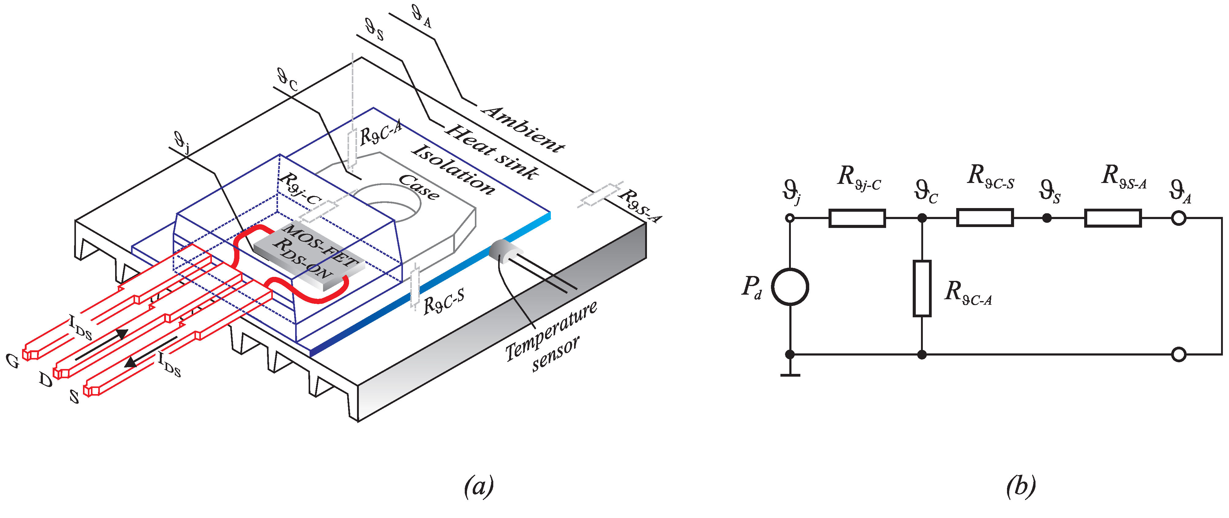
As can be seen from Equation (
4),
contains two parts; the conductive
and switching
losses. Conductive losses are deterministic for small currents and can be calculated as follows:
where
is transistor voltage, when the transistor is conducting the current
, and
δ is a duty cycle ratio. At higher currents, the MOS-FET’s terminals and bonding wires also heat-up significantly (they are insulated within plastic housing). The interesting fact is also that the current value
is unknown during power dissipation calculation, because the value itself is a result of a measurement algorithm. Therefore, in order to evaluate
, it is necessary to use the current measured over previous switching period, which causes the inaccuracy of the measurement procedure. The second part of the losses are the switching losses, which are even harder to evaluate. Different equations exist, but they do not consider all of the effects within the measurement circuit. In a real circuit, the parasitic inductances and capacitances of tracks and elements cause oscillations in the currents and voltages, and this results in some additional switching losses.
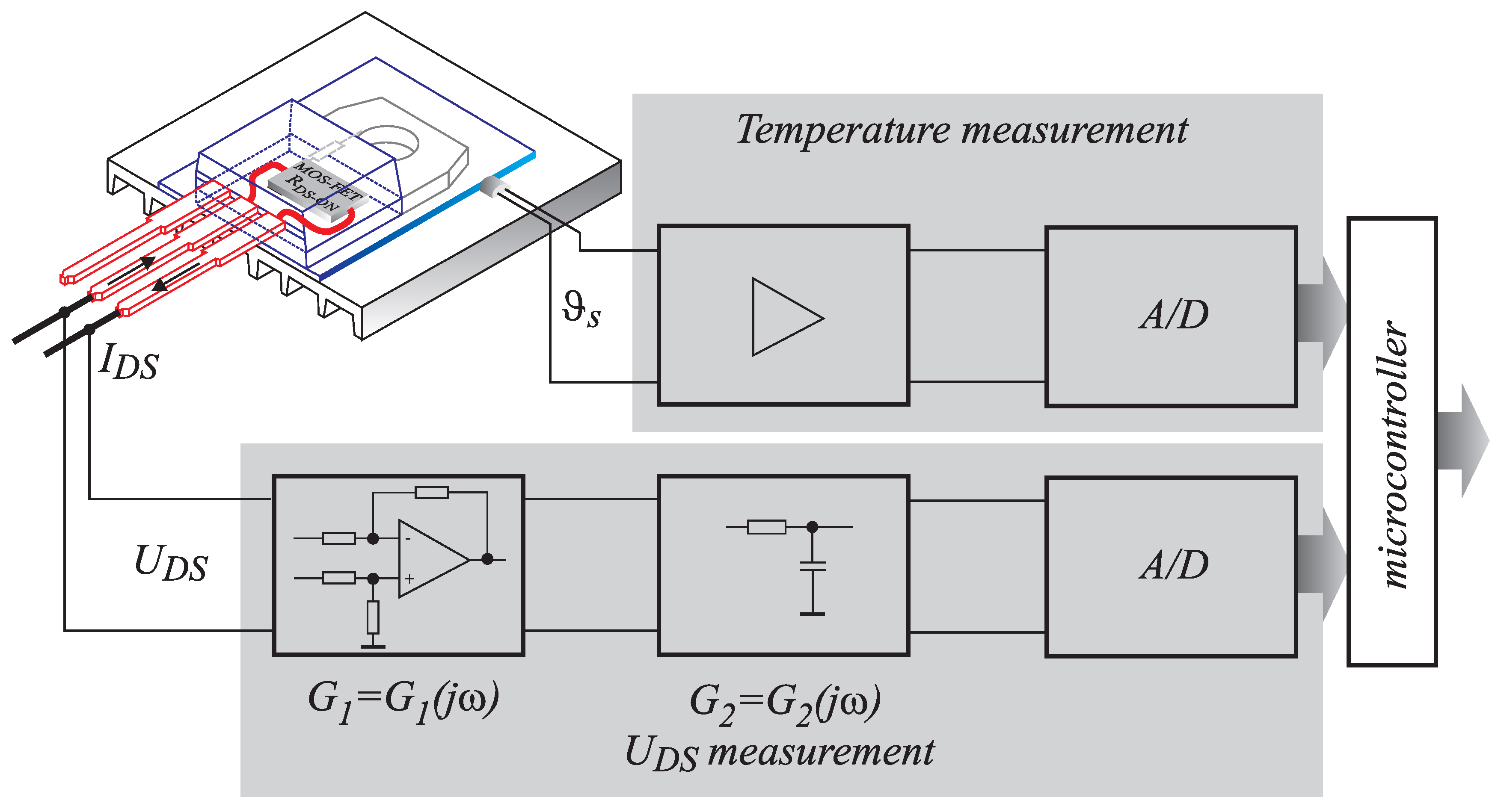
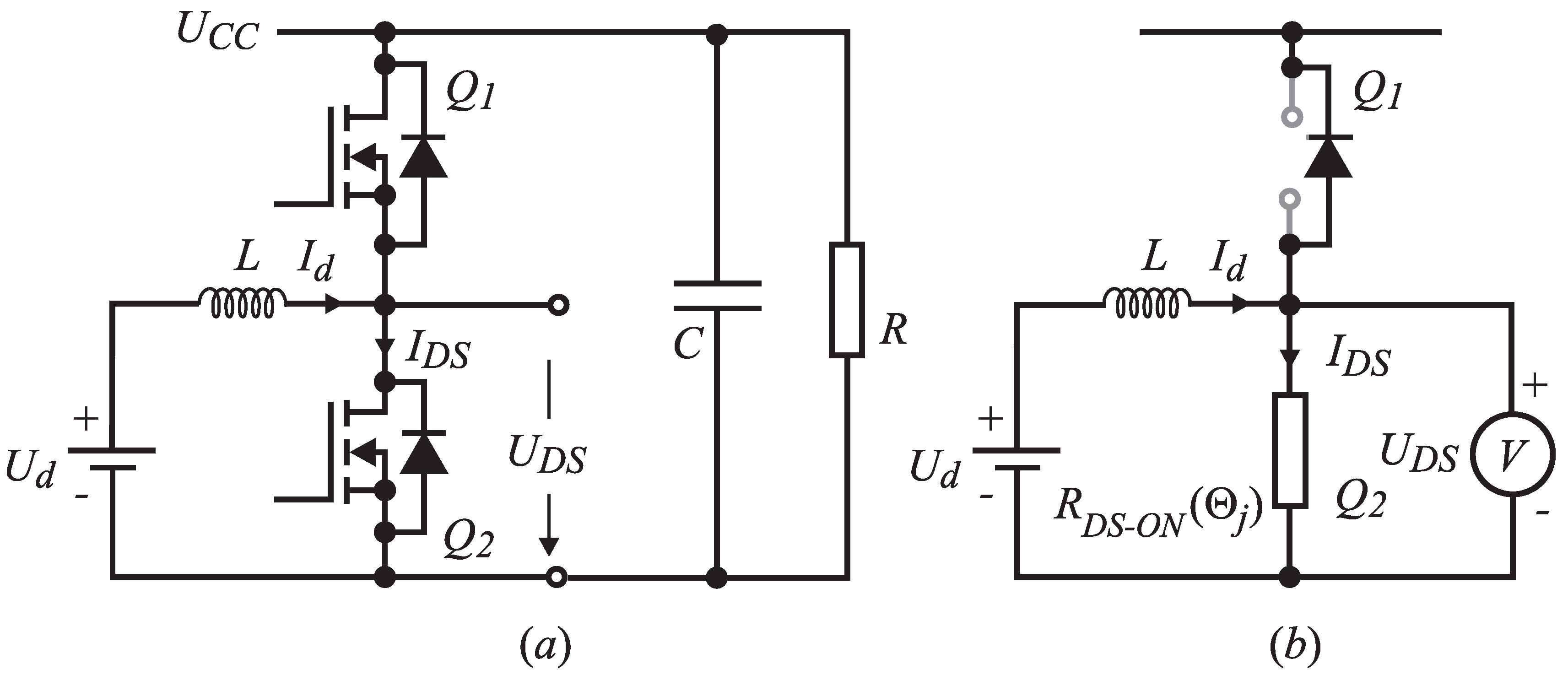
Figure 6 shows these inductances and capacitances on the boost converter circuit example. As switching losses calculation is always an approximation, they were measured with an oscilloscope. During MOS-FET turn-on and turn-off, the currents and voltages on the terminals were measured simultaneously.
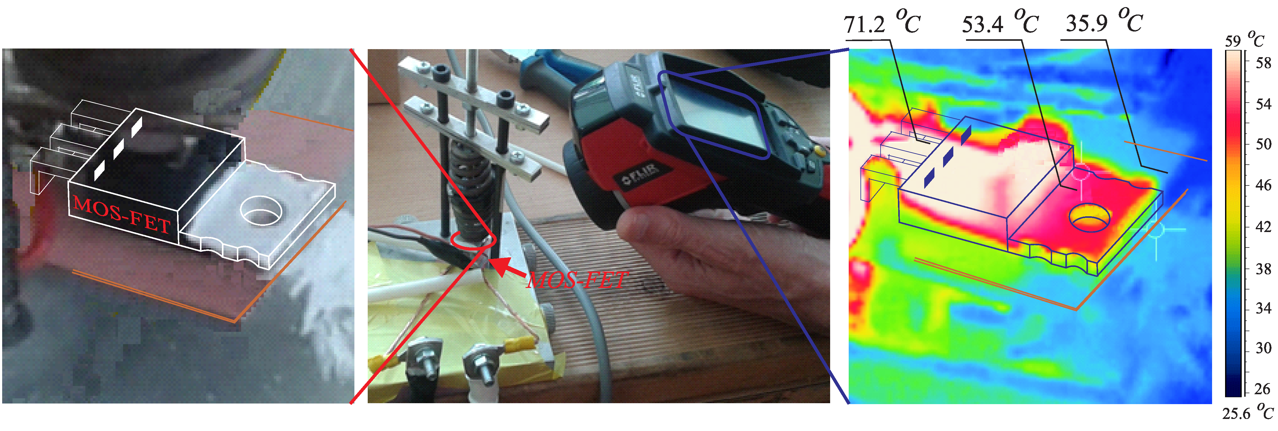
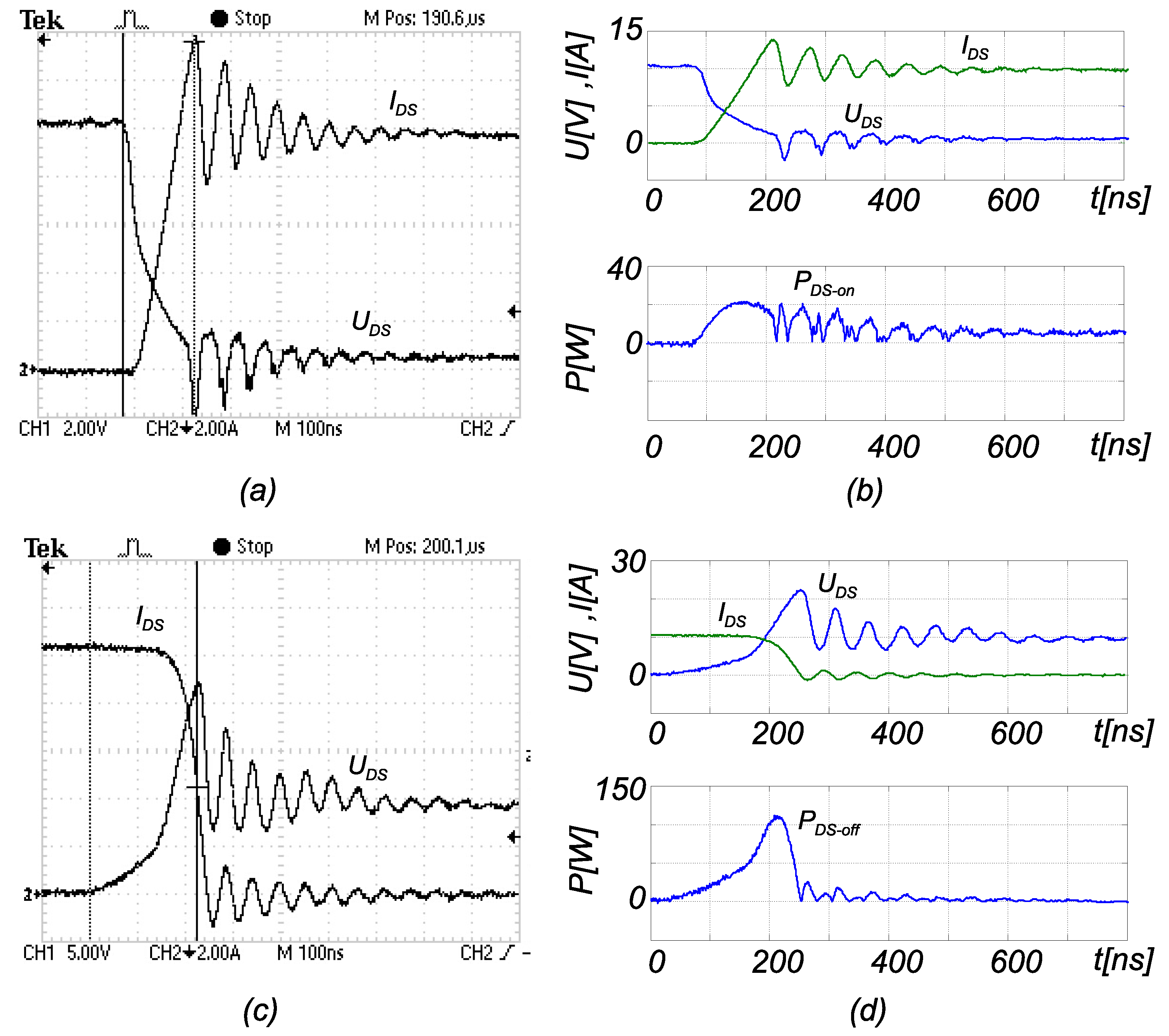
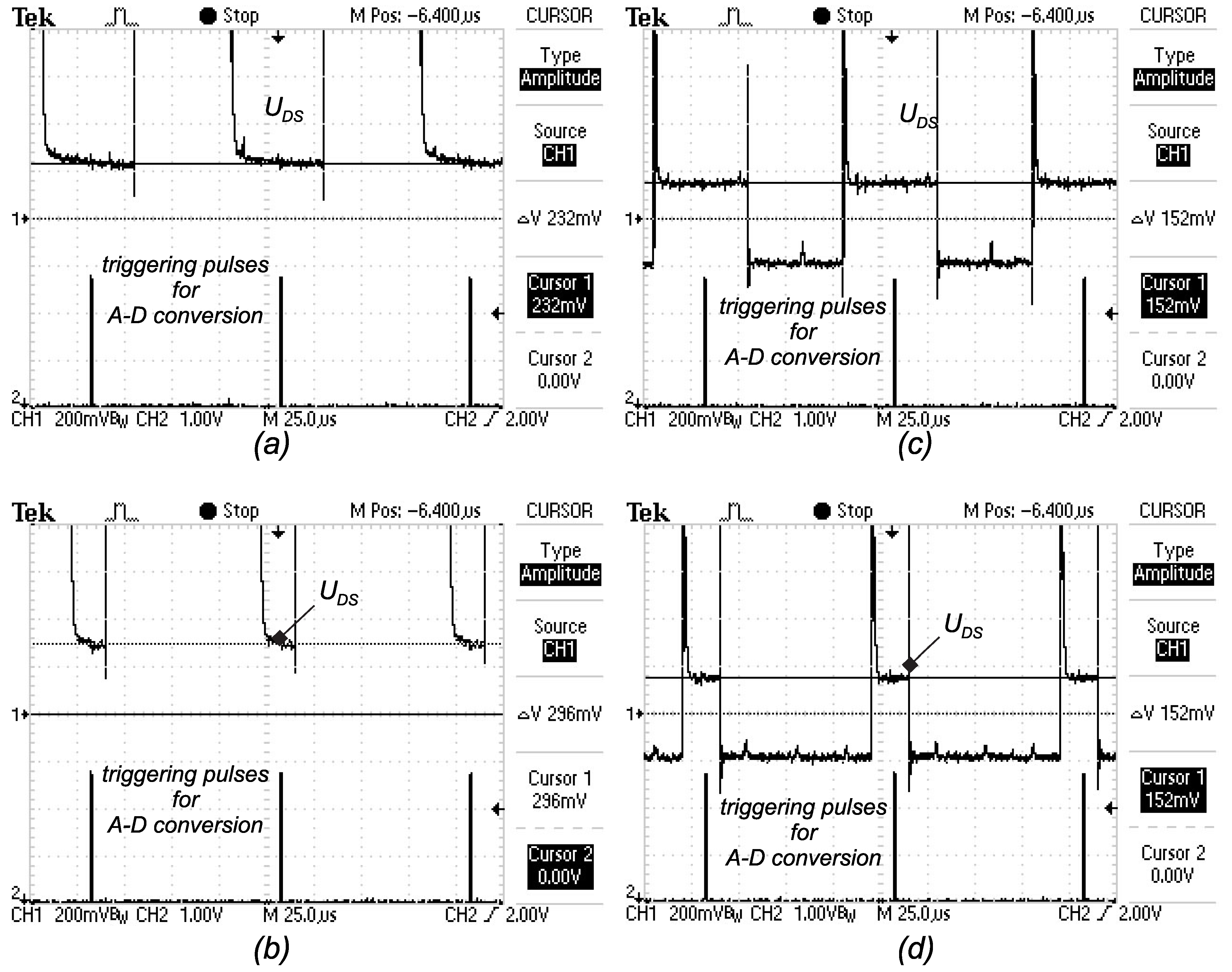
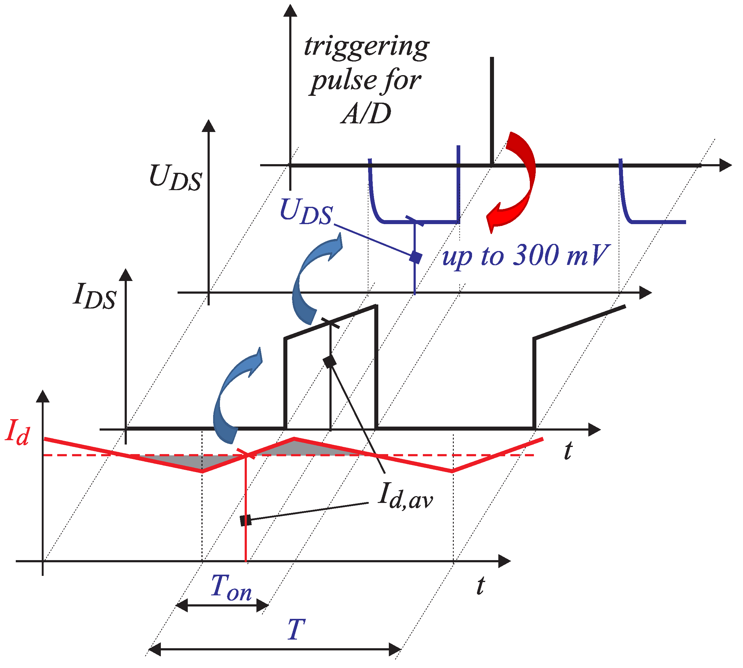
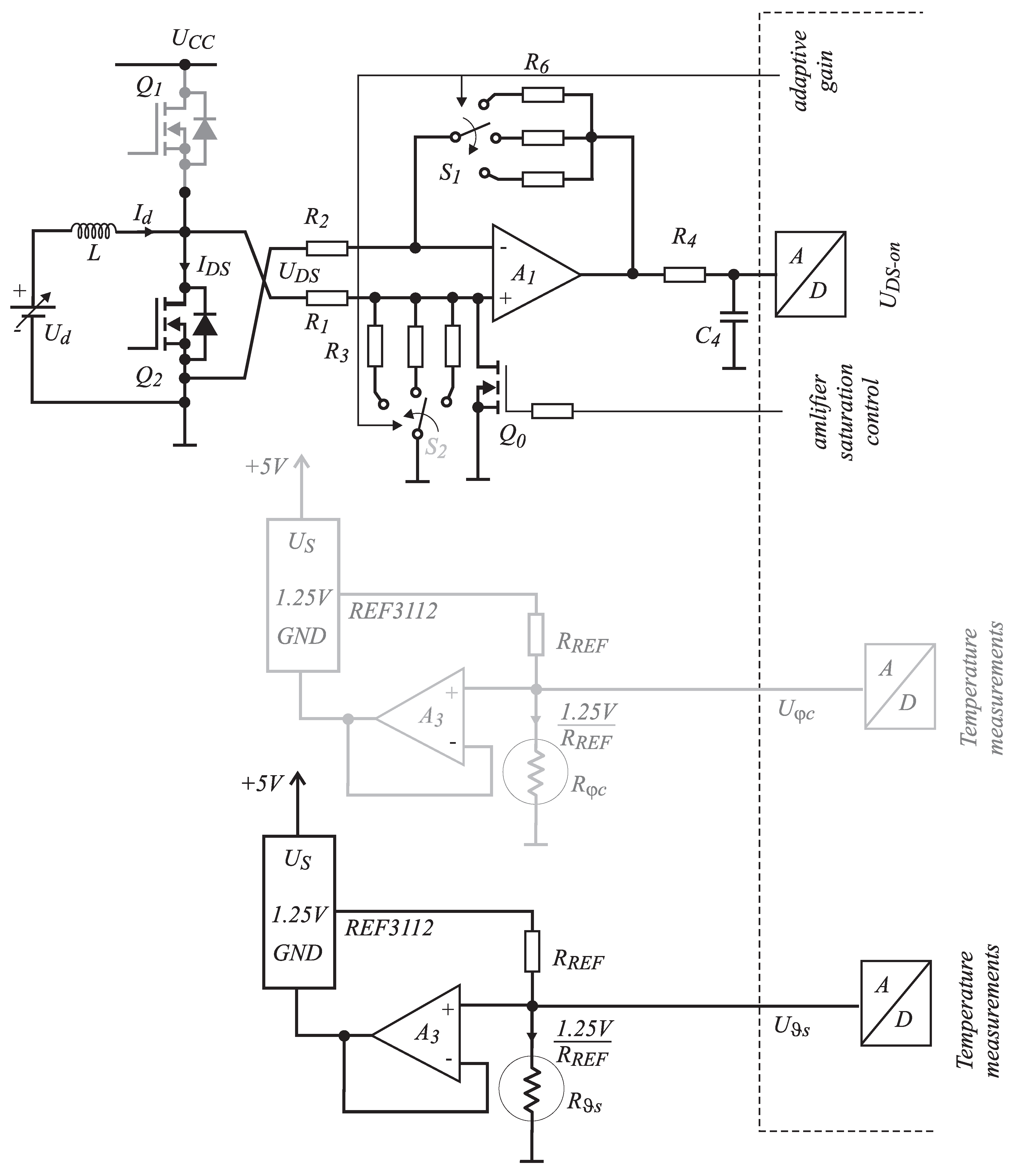
Figure 7 shows waveforms during MOS-FET turn-off at the current of 10 A and supply voltage of 10 V. The waveforms were recorded with a Tektronix oscilloscope, that has a bandwidth of 100 MHz, and the current probe was Tektronix TCP305A with amplifier TCPA300. The probe’s bandwidth is 50 MHz, and the signal propagation delay is 19 ns. The problem also occurs in the
voltage measurement, that is inaccurate because of the parasitic inductances of terminals and bonding wires in the transistor. The switching losses were calculated from the acquired waveforms, by using:
where
and
are the instantaneously-measured voltage and current values over equidistant time intervals of
. Index
suggests that the equation can be used in turn-on or turn-off cases. The data were obtained from the oscilloscope in the form of a CSV (Comma Separated Value) file and transferred to MATLAB for further processing. The calculation was performed under the MATLAB framework, where the current signal delay had also to be accounted for by moving the waveform left, considering the propagation delay of 19 ns. In
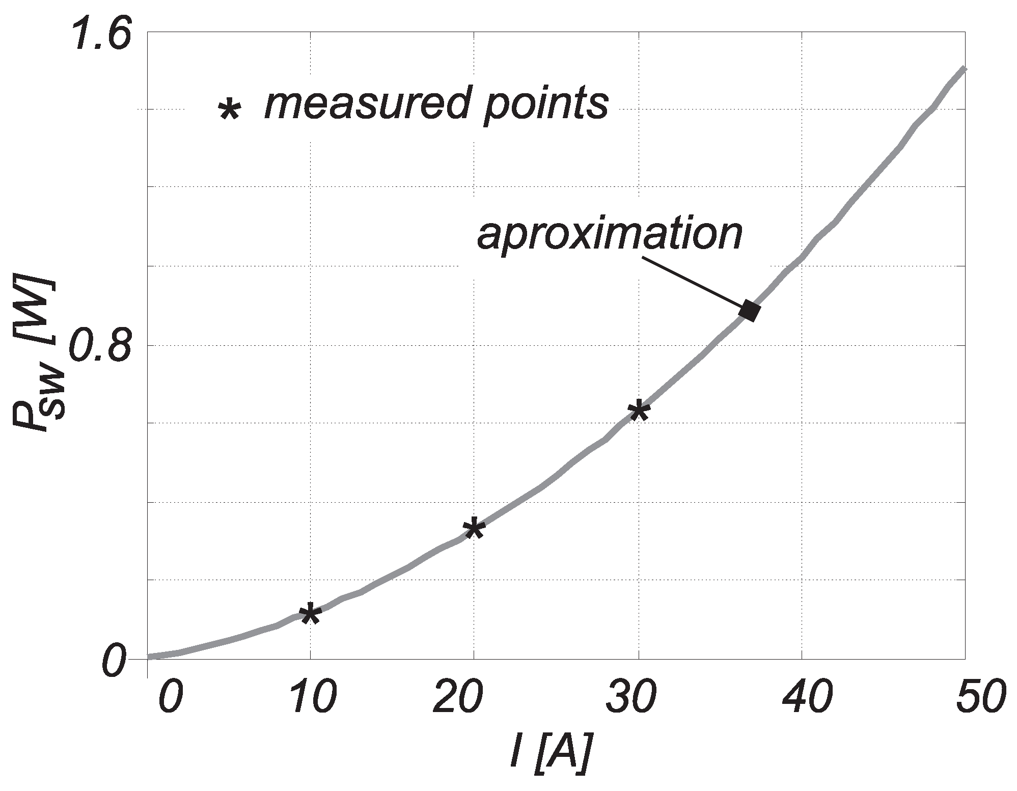
Figure 7b,d, the instantaneous losses’ waveforms’ are shown during the switching on and off. The total value of the switching losses was calculated by Equation (
10). This procedure was used to measure the turn-on and turn-off losses at three different currents
A, as collected in
Table 4.
Figure 8 shows the switching losses depending on current
(
), when the voltage is kept constant at 10 V. It was approximated by a second order polynomial, calculated from the measurement results from
Table 4 as follows:
Figure 6.
Parasitic elements in the boost converter.
Figure 7.
MOS-FET’s turn-on/-off waveforms; (a) oscillogram of voltage and current during the switching-on; (b) oscillogram exported to the MATLAB frame for the calculation of switching on dissipation; (c) oscillogram of voltage and current during the switching off; (d) oscillogram exported to the MATLAB frame for calculation of switching off dissipation.
Figure 8.
The MOS-FET’s switching losses.
The constant supply voltage is assumed for power converters. When powered from batteries, the voltage can vary, but within a narrow range.


