Article

Aqueous Solution-Grown Crystalline Phosphorus Doped Indium Oxide for Thin-Film Transistors Applications

1
Department of Physics, School of Science, Jimei University, Xiamen 361021, China
2
College of Materials Science and Engineering, Shenzhen University, Shenzhen 518000, China
3
Shenzhen Key Laboratory of Ultraintense Laser and Advanced Material Technology, Center for Advanced Material Diagnostic Technology, and College of Engineering Physics, Shenzhen Technology University, Shenzhen 518118, China
4
Department of Electrical and Electronic Engineering, Xi’an Jiaotong-Liverpool University, Suzhou 215123, China
*
Authors to whom correspondence should be addressed.
Int. J. Mol. Sci. 2022, 23(21), 12912; https://doi.org/10.3390/ijms232112912
Submission received: 6 September 2022 / Revised: 20 October 2022 / Accepted: 23 October 2022 / Published: 26 October 2022

Abstract

:
Solution-grown indium oxide (In2O3) based thin-film transistors (TFTs) hold good prospects for emerging advanced electronics due to their excellent mobility, prominent transparency, and possibility of low-cost and scalable manufacturing; however, pristine In2O3 TFTs suffer from poor switching characteristics due to intrinsic oxygen-vacancy-related defects and require external doping. According to Shanmugam’s theory, among potential dopants, phosphorus (P) has a large dopant–oxygen bonding strength (EM-O) and high Lewis acid strength (L) that would suppress oxygen-vacancy related defects and mitigate dopant-induced carrier scattering; however, P-doped In2O3 (IPO) TFTs have not yet been demonstrated. Here, we report aqueous solution-grown crystalline IPO TFTs for the first time. It is suggested that the incorporation of P could effectively inhibit oxygen-vacancy-related defects while maintaining high mobility. This work experimentally demonstrates that dopant with high EM-O and L is promising for emerging oxide TFTs.

1. Introduction

Transparent oxide semiconductors have emerged as promising materials for a wide range of applications, including thin-film transistors (TFTs) [1,2,3]; besides, oxide semiconductors could be solution-processed in an ambient atmosphere, showing great potential for scalable manufacturing [4,5,6,7,8]. In2O3 is a representative transparent oxide semiconductor with high mobility due to the large overlap of In 5 s orbital; however, the low binding energy of In-O (320.1 KJ/mol) favors oxygen-vacancy formation, resulting in high carrier density [9]. This often leads to high off-state-current and poor subthreshold swing when used as channel material for TFT applications. Previous investigations suggest that doping/alloying is an effective approach to solve this issue [10,11,12,13,14,15,16,17].
Based on Shanmugam’s theory, a promising dopant should have a large dopant–oxygen bonding strength (EM-O) and high Lewis acid strength (L) [11,12]. The large EM-O is able to suppress oxygen-vacancy related defects; however, the introduction of extrinsic dopant would act as scattering centers, causing a drop in mobility [12]. The L can be described as: L = Z/r2 −7.7χz + 8.0, where Z represents the atomic nucleus charge number, r is the ionic radius, and χz designates the element electronegativity [12]. The high L could polarize electron charge away from the oxygen 2p valence band, weakening its activity as scattering centers and, hence, maintaining high mobility [11,12]; therefore, large EM-O and high L are essential for the dopant element. Table 1 tabulated the EM-O and L of common dopants for In2O3 host metal oxides [12]. Of all the potential dopants, phosphorus (P) has a large EM-O (599.1 KJ/mol) and high L (10.082), showing great potential for controlling oxygen-vacancy related defects and alleviating dopant impurity carrier scattering. Unfortunately, P-doped In2O3 (IPO) TFTs have not yet been demonstrated and, hence, are worth investigating.
In this contribution, we first report the use of P as an efficient dopant for In2O3 TFTs. The IPO channel is fabricated via an aqueous solution route, which enables potential low-cost and expedient manufacturing. The impact of P incorporation is thoroughly investigated. The results show that the incorporation of P could effectively inhibit oxygen-vacancy-related defects while maintaining good mobility. The optimized IPO device (6% P) shows a decent mobility of 6.33 cm2/V s, threshold voltage of 2.97 V, subthreshold swing of 0.60 V/dec, and an excellent ION/OFF of ~108, respectively.

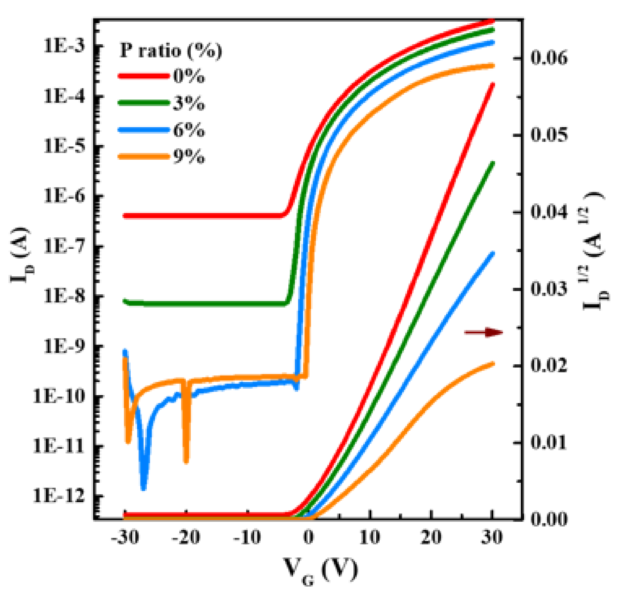
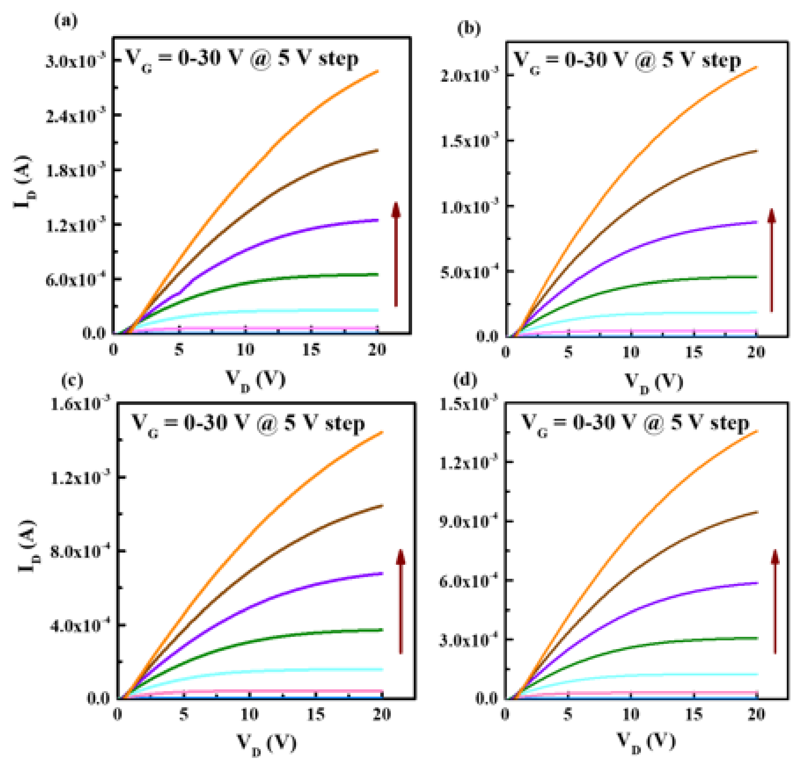
2. Results and Discussion

We performed grazing incidence XRD diffraction analysis on the crystalline structure of IPO films with different P proportions. As shown in Figure 1, the broad peaks at ~22.4° are attributed to the substrate. The characteristic diffraction peaks of (222) (dominant peak), (400), (440), and (622) are assignable to bixbyite In2O3 (JCPDS 06-0416). No P2O5 or other phases are observed from the diffraction pattern, which means that P addition does not break the In2O3 matrix crystalline structure [18,19]. We suppose that the added P replaces the In sites and maintains the cubic In2O3 structure when the P doping amount is relatively low; however, the diffraction peak intensity gradually decreases, suggesting the reduction of crystallinity after P incorporation [20]. This is because the P element would enhance the local distortions of the InO polyhedral and suppress the number of coordinate In atoms [13,20]. Previous studies also suggest that the addition of different-sized metal cations into the In2O3 could destroy the In2O3 lattice and reduce the crystallinity [10,11,13,20].
AFM measurements shown in Figure 2 indicate that the series of IPO films are highly smooth with RMS roughness of 0.27, 0.24, 0.31, and 0.26 nm for P ratio of 0, 3, 6, and 9%, respectively. The results suggest the absence of prominent grain boundaries in the crystalline IPO films and that P doping has little impact on the surface topography. It should be mentioned that the atomic smooth surface of the channel material is essential for transistor applications.
Figure 3a represents the optical transmittance spectra of IPO films with a range of P-doping contents. All the IPO films demonstrate excellent transparency (>79% at a wavelength of 550 nm). By using Tauc equation, the optical bandgaps of IPO films (Figure 3b) are calculated to be 3.61 eV (0% P), 3.66 eV (3% P), 3.88 eV (6% P), and 4.19 eV (9% P), respectively. The increased bandgap with P addition could be due to the fact that P can inhibit the formation of oxygen-vacancy defects in In2O3 [19]. The increased bandgap is more in line with the larger binding strength of P-O (599.1 KJ/mol) than that of In-O bonding (320.1 KJ/mol), indicating the effective oxygen-vacancy-related defects suppression [21].
XPS is supplemented for further verification. The corresponding P 2p spectra were demonstrated in Figure 4a. Previous reports have summarized the P 2p peak energies [22]. The peaks at ~135.6 eV, 133.5 eV, 128.6 eV, and 129.9 eV correspond to P2O5, phosphate, phosphide, and elemental P, respectively [22]; therefore, in the present work, the characteristic peak at ~133.5 eV is assigned to phosphate (PO43-). In addition, as shown in Figure 4b, the P/In+ P ratio in the thin film steadily increases from 0 to 3.1, 5.6, and 8.4%, as the P ratio in the precursor increases from 0 to 3%, 6%, and 9%, respectively.
Figure 5 and Figure 6 show the representative transfer and output curves of the IPO TFTs with different P ratios, with electrical parameters summarized in Table 2. The pristine In2O3 TFT shows a good mobility of 16.2 cm2/V s, but high off-state current and poor subthreshold slope, which is typical behavior for an undoped-In2O3 device. The P incorporation leads to the great improvement of off-state-current and subthreshold swing, as well as positive shift of threshold voltage; besides, the trap density (including interface and bulk region, see Table 2) also improves after P incorporation, indicating that P doping weakens carrier scattering in IPO [23]. This is because the addition of P could inhibit the oxygen-vacancy-related defects due to the larger EM-O.
Unfortunately, P introduction would reduce the In 5 s orbital interaction near the conduction band, and, hence, decrease the mobility [10]; however, P has a high Lewis acid strength L, which could polarize electron charge away from the oxygen 2p valence band, weakening carrier scattering centers and, hence, relatively high mobility could be maintained [11,12]. The overall best IPO device (6% P) demonstrates a μ of 6.33 cm2/V s, Ion/Ioff of 1.1 × 10⁸, S of 0.60 V/dec, and Vth of 2.97 V, respectively, which is sufficient for transistor applications. The mobility of 6.33 cm2/Vs is relatively high since mobility larger than 5 cm2/V s is sufficient for liquid crystal display (LCD) applications (the mobility of commercial a-Si is 1 cm2/V s). Although P doping reduces the mobility of pristine In2O3, the other device parameters, especially on/off ratio, is greatly improved.
As shown in Table 3, we have provided the comparison with reported IGZO-related devices in the literature. Our newly designed IPO TFTs are among some of the best results. The newly designed IPO TFTs can be used in flat-panel displays and non-display applications, such as biosensors, photodetectors, memory, and neuromorphic devices.

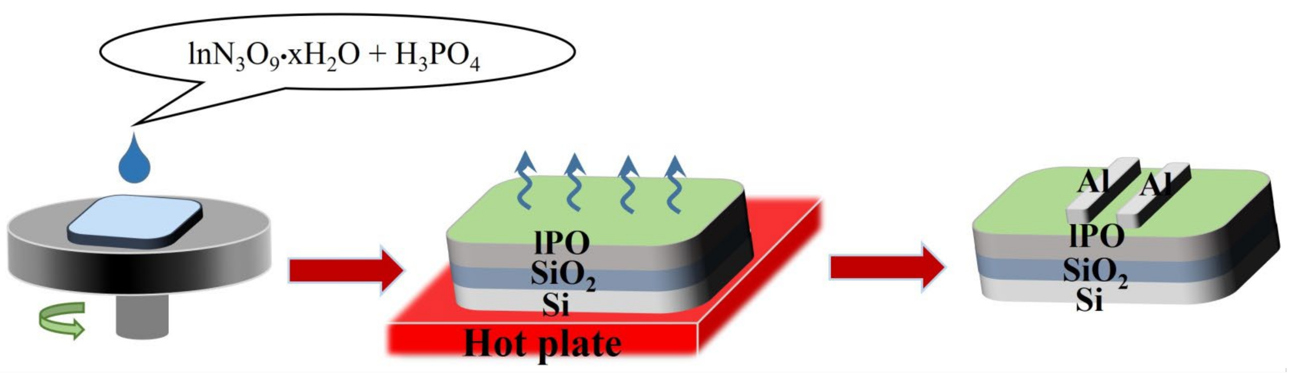
3. Experimental Section

Indium nitrate and phosphoric acid were dissolved in DI water with total concentration of 0.2 M and stirred for 2 h before deposition. The desired P/(In + P) atomic contents of 0, 3, 6, and 9% were produced. The IPO layers (~6 nm) were one-step spun at 4500 r.p.m. for 30 s on Si/SiO2 substrates and, then, thermally annealed at 300 °C for 120 min in ambient air. IPO TFTs (W/L = 1500/100 μm) fabrications were completed by evaporating Al source and drain electrodes. The IPO TFT device fabrication process is shown in Figure 7.
Grazing incidence XRD was performed on a Rigaku workstation (Austin, TX, USA). The surface topography information of IPO film was measured via AFM using Bruker Dimension Icon (Beijing, China). The chemical bonding states of IPO were analyzed via X-ray photoelectron spectroscopy (XPS, Thermo Microlab 350, Antigo, WI, USA). The transmittance information of the IPO layer was observed by UV-Vis spectrophotometry with PerkinElmer Lambda 950 (Waltham, MA, USA). Electrical current-voltage measurements of the transistors were carried out in air with a Keithley 2614B digital source meter (San Diego, CA, USA).

4. Conclusions

An efficient and tunable aqueous approach is reported to enhance In2O3 TFTs performance via P doping. It is suggested that P doping in In2O3 TFTs could suppress oxygen-vacancy-related defects that cause electron generation and trapping. The optimal IPO TFTs show enhanced switching characteristics. This work experimentally demonstrates that dopant with high dopant–oxygen bonding strength and Lewis acid strength is a promising candidate and opens a new way to fabricate high performance TFTs at low processing temperature.

Author Contributions

Conceptualization, W.X.; Funding acquisition, W.X. and F.X.; Investigation; T.P. and Y.L.; Project administration, W.X.; Supervision, W.X.; Writing—original draft, W.X.; Writing—review & editing, W.X., S.Z., Q.L., W.H., F.X., C.Z. and D.Z. All authors have read and agreed to the published version of the manuscript.

Funding

This research was funded by the National Natural Science Foundation of China (61704111, 12074263 and 62001308), the Scientific Research Starting Foundation of Jimei University (C622124), and the Natural Science Foundation of Top Talent of SZTU (20200219).

Conflicts of Interest

The authors declare no conflict of interest.

References

  1. Fortunato, E.; Barquinha, P.; Martins, R. Oxide semiconductor thin-film transistors: A review of recent advances. Adv. Mater. 2012, 24, 2945–2986. [Google Scholar] [CrossRef] [PubMed]
  2. Yu, X.; Marks, T.J.; Facchetti, A. Metal oxides for optoelectronic applications. Nat. Mater. 2016, 15, 383–396. [Google Scholar] [CrossRef] [PubMed]
  3. Kamiya, T.; Hosono, H. Material characteristics and applications of transparent amorphous oxide semiconductors. NPG Asia Mater. 2010, 2, 15–22. [Google Scholar] [CrossRef] [Green Version]
  4. Xu, W.; Li, H.; Xu, J.B.; Wang, L. Recent Advances of Solution-Processed Metal Oxide Thin-Film Transistors. ACS Appl. Mater. Interfaces 2018, 10, 25878–25901. [Google Scholar] [CrossRef]
  5. Chen, R.; Lan, L. Solution-processed metal-oxide thin-film transistors: A review of recent developments. Nanotechnology 2019, 30, 312001. [Google Scholar] [CrossRef]
  6. Cochran, E.A.; Woods, K.N.; Johnson, D.W.; Page, C.J.; Boettcher, S.W. Unique chemistries of metal-nitrate precursors to form metal-oxide thin films from solution: Materials for electronic and energy applications. J. Mater. Chem. A 2019, 7, 24124–24149. [Google Scholar] [CrossRef]
  7. Park, J.W.; Kang, B.H.; Kim, H.J. A Review of Low-Temperature Solution-Processed Metal Oxide Thin-Film Transistors for Flexible Electronics. Adv. Funct. Mater. 2019, 30, 1904632. [Google Scholar] [CrossRef]
  8. Hwan Hwang, Y.; Seo, J.-S.; Moon Yun, J.; Park, H.; Yang, S.; Ko Park, S.-H.; Bae, B.-S. An ‘aqueous route’ for the fabrication of low-temperature-processable oxide flexible transparent thin-film transistors on plastic substrates. NPG Asia Mater. 2013, 5, e45. [Google Scholar] [CrossRef] [Green Version]
  9. Lee, J.; Moon, J.; Pi, J.-E.; Ahn, S.-D.; Oh, H.; Kang, S.-Y.; Kwon, K.-H. High mobility ultra-thin crystalline indium oxide thin film transistor using atomic layer deposition. Appl. Phys. Lett. 2018, 113, 112102. [Google Scholar] [CrossRef]
  10. Li, Y.; Zhu, D.; Xu, W.; Han, S.; Fang, M.; Liu, W.; Cao, P.; Lu, Y. High-mobility nanometer-thick crystalline In–Sm–O thin-film transistors via aqueous solution processing. J. Mater. Chem. C 2020, 8, 310–318. [Google Scholar] [CrossRef]
  11. Zhang, X.; Wang, B.; Huang, W.; Chen, Y.; Wang, G.; Zeng, L.; Zhu, W.; Bedzyk, M.J.; Zhang, W.; Medvedeva, J.E.; et al. Synergistic Boron Doping of Semiconductor and Dielectric Layers for High-Performance Metal Oxide Transistors: Interplay of Experiment and Theory. J. Am. Chem. Soc. 2018, 140, 12501–12510. [Google Scholar] [CrossRef]
  12. Parthiban, S.; Kwon, J.-Y. Role of dopants as a carrier suppressor and strong oxygen binder in amorphous indium-oxide-based field effect transistor. J. Mater. Res. 2014, 29, 1585–1596. [Google Scholar] [CrossRef] [Green Version]
  13. Smith, J.; Zeng, L.; Khanal, R.; Stallings, K.; Facchetti, A.; Medvedeva, J.E.; Bedzyk, M.J.; Marks, T.J. Cation Size Effects on the Electronic and Structural Properties of Solution-Processed In-X-O Thin Films. Adv. Electron. Mater. 2015, 1, 1500146. [Google Scholar] [CrossRef]
  14. Li, Y.; Xu, W.; Liu, W.; Han, S.; Cao, P.; Fang, M.; Zhu, D.; Lu, Y. High-Performance Thin-Film Transistors with Aqueous Solution-Processed NiInO Channel Layer. ACS Appl. Electron. Mater. 2019, 1, 1842–1851. [Google Scholar] [CrossRef]
  15. Kim, H.J.; Je, S.Y.; Won, J.Y.; Baek, J.H.; Jeong, J.K. Effect of antimony doping on the low-temperature performance of solution-processed indium oxide thin film transistors. Phys. Status Solidi (RRL)-Rapid Res. Lett. 2014, 8, 924–927. [Google Scholar] [CrossRef]
  16. Kim, T.; Jang, B.; Lee, S.; Lee, W.Y.; Jang, J. Improved Negative Bias Stress Stability of Sol-Gel-Processed Mg-Doped In2O3 Thin Film Transistors. IEEE Electron Device Lett. 2018, 39, 1872–1875. [Google Scholar] [CrossRef]
  17. Kim, Y.G.; Kim, T.; Avis, C.; Lee, S.H.; Jang, J. Stable and High-Performance Indium Oxide Thin-Film Transistor by Ga Doping. IEEE Trans. Electron Devices 2016, 63, 1078–1084. [Google Scholar] [CrossRef]
  18. Xu, W.; Xu, C.; Hong, L.; Xu, F.; Zhao, C.; Zhang, Y.; Fang, M.; Han, S.; Cao, P.; Lu, Y.; et al. Aqueous Solution-Processed Nanometer-Thin Crystalline Indium Ytterbium Oxide Thin-Film Transistors. Nanomaterials 2022, 12, 1216. [Google Scholar] [CrossRef]
  19. Xu, W.; Peng, T.; Li, Y.; Xu, F.; Zhang, Y.; Zhao, C.; Fang, M.; Han, S.; Zhu, D.; Cao, P.; et al. Water-Processed Ultrathin Crystalline Indium-Boron-Oxide Channel for High-Performance Thin-Film Transistor Applications. Nanomaterials 2022, 12, 1125. [Google Scholar] [CrossRef]
  20. Hong, L.; Xu, W.; Liu, W.; Han, S.; Cao, P.; Fang, M.; Zhu, D.; Lu, Y. High performance indium dysprosium oxide thin-film transistors grown from aqueous solution. Appl. Surf. Sci. 2020, 504, 144499. [Google Scholar] [CrossRef]
  21. Park, H.; Nam, Y.; Jin, J.; Bae, B.-S. Improvement of bias stability of oxyanion-incorporated aqueous sol–gel processed indium zinc oxide TFTs. J. Mater. Chem. C 2014, 2, 5998–6003. [Google Scholar] [CrossRef]
  22. Wager, J.F.; Ellsworth, D.L.; Goodnick, S.M.; Wilmsen, C.W. Composition and thermal stability of thin native oxides on InP. J. Vac. Sci. Technol. 1981, 19, 513–518. [Google Scholar] [CrossRef]
  23. Luo, D.; Lan, L.; Xu, M.; Xu, H.; Li, M.; Wang, L.; Peng, J. Role of Rare Earth Ions in Anodic Gate Dielectrics for Indium-Zinc-Oxide Thin-Film Transistors. J. Electrochem. Soc. 2012, 159, H502–H506. [Google Scholar] [CrossRef]
  24. Banger, K.K.; Yamashita, Y.; Mori, K.; Peterson, R.L.; Leedham, T.; Rickard, J.; Sirringhaus, H. Low-temperature, high-performance solution-processed metal oxide thin-film transistors formed by a ‘sol-gel on chip’ process. Nat. Mater. 2011, 10, 45–50. [Google Scholar] [CrossRef]
  25. Wang, B.; Zeng, L.; Huang, W.; Melkonyan, F.S.; Sheets, W.C.; Chi, L.; Bedzyk, M.J.; Marks, T.J.; Facchetti, A. Carbohydrate-Assisted Combustion Synthesis To Realize High-Performance Oxide Transistors. J. Am. Chem. Soc. 2016, 138, 7067–7074. [Google Scholar] [CrossRef]
  26. Yu, X.; Smith, J.; Zhou, N.; Zeng, L.; Guo, P.; Xia, Y.; Alvarez, A.; Aghion, S.; Lin, H.; Yu, J.; et al. Spray-combustion synthesis: Efficient solution route to high-performance oxide transistors. Proc. Natl. Acad. Sci. USA 2015, 112, 3217–3222. [Google Scholar] [CrossRef] [Green Version]
  27. Rim, Y.S.; Jeong, W.H.; Kim, D.L.; Lim, H.S.; Kim, K.M.; Kim, H.J. Simultaneous modification of pyrolysis and densification for low-temperature solution-processed flexible oxide thin-film transistors. J. Mater. Chem. 2012, 22, 12491–12497. [Google Scholar] [CrossRef]
  28. Yoon, S.; Kim, S.J.; Tak, Y.J.; Kim, H.J. A solution-processed quaternary oxide system obtained at low-temperature using a vertical diffusion technique. Sci. Rep. 2017, 7, 43216. [Google Scholar] [CrossRef] [Green Version]
  29. Kim, Y.H.; Heo, J.S.; Kim, T.H.; Park, S.; Yoon, M.H.; Kim, J.; Oh, M.S.; Yi, G.R.; Noh, Y.Y.; Park, S.K. Flexible metal-oxide devices made by room-temperature photochemical activation of sol-gel films. Nature 2012, 489, 128–132. [Google Scholar] [CrossRef]
Figure 1. Grazing incidence XRD patterns for IPO films with indicated P ratio.
Ijms 23 12912 g001
Figure 2. AFM images of the surface topography of IPO films with indicated P ratio of (a) 0%, (b) 3%, (c) 6%, and (d) 9%.
Ijms 23 12912 g002
Figure 3. (a) Optical transmittance spectra of IPO films with various P ratios, and (b) corresponding optical bandgaps derived from the Tauc plots.
Ijms 23 12912 g003
Figure 4. XPS spectra for the IPO films with different P-doping contents. (a) P 2p. spectra, and (b) P-doping ratio between solution and film.
Ijms 23 12912 g004
Figure 5. Transfer characteristics measured for IPO TFTs with different P ratios.
Ijms 23 12912 g005
Figure 6. Output characteristics measured for IPO TFTs with P ratios of (a) 0%, (b) 3%, (c) 6%, and (d) 9%.
Ijms 23 12912 g006
Figure 7. The IPO TFT device fabrication process.
Ijms 23 12912 g007
Table 1. Metal-oxygen bonding strength (EM-O) and Lewis acid strength (L) of elements.
ElementsMetal-Oxygen Bonding
Strength (EM-O, KJ/mol)
Lewis Acid
Strength (L)
In3+320.11.026
Ga3+353.51.167
Ba2+502.91.163
Mg2+363.21.402
Al3+511.03.042
Sb5+434.33.559
P5+599.110.082
Table 2. Summary of electrical properties of IPO TFTs investigated.
P Ratio
(%)
Mobility
(cm2/V s)
On/Off
Ratio
Threshold
Voltage (V)
Subthreshold Swing (V/dec)Trap Densities
(cm−2 eV−1)
016.23.8 × 103−0.572.528.6 × 1012
310.83.1 × 1051.980.972.9 × 1012
66.331.1 × 1082.970.601.4 × 1012
93.526.4 × 1073.270.551.2 × 1012
Table 3. Recent advances of solution-processed IGZO-related TFTs.
Channel
Material
μ
(cm2/Vs)
Ion/IoffRef
IZO4107[24]
IGZO7.5107[25]
IGZO8.05107[26]
IZO2.43107[27]
IGZO1.38105[28]
IGZO2.64108[29]
IPO6.33108This work
Publisher’s Note: MDPI stays neutral with regard to jurisdictional claims in published maps and institutional affiliations.

