Abstract
This study proposes a high-performance organic–inorganic hybrid memristor for the development of neuromorphic devices in the memristor-based artificial synapse. The memristor consists of a solid polymer electrolyte (SPE) chitosan layer and a titanium oxide (TiOx) layer grown with a low-thermal-budget, microwave-assisted oxidation. The fabricated Ti/SPE–chitosan/TiOx/Pt-structured memristor exhibited steady bipolar resistive switching (BRS) characteristics and demonstrated excellent endurance in 100-cycle repetition tests. Compared to SPE–chitosan memristors without a TiOx layer, the proposed organic–inorganic hybrid memristor demonstrated a higher dynamic range and a higher response to pre-synaptic stimuli such as short-term plasticity via paired-pulse facilitation. The effect of adding the TiOx layer on the BRS properties was examined, and the results showed that the TiOx layer improved the chemical and electrical superiority of the proposed memristor synaptic device. The proposed SPE–chitosan organic–inorganic hybrid memristor also exhibited a stable spike-timing-dependent plasticity, which closely mimics long-term plasticity. The potentiation and depression behaviors that modulate synaptic weights operated stably via repeated spike cycle tests. Therefore, the proposed SPE–chitosan organic–inorganic hybrid memristor is a promising candidate for the development of neuromorphic devices in memristor-based artificial synapses owing to its excellent stability, high dynamic range, and superior response to pre-synaptic stimuli.
1. Introduction
Current state-of-the-art computing systems face enormous challenges when dealing with large amounts of unstructured data and real-time decision-making processes because of the von Neumann bottleneck limitations [1,2], which have necessitated the development of new intelligent computing platforms that can overcome these limitations. One such platform is the two-terminal metal-insulator-metal (MIM) structure memristor, which offers several advantages such as simplicity, nonvolatile memory, and computations using consecutive analog resistive switching (RS) in the insulator layer [3,4,5]. Several studies have investigated the development of computing systems capable of performing complex computations based on analog RS. The synaptic plasticity RS layer of memristors has been extensively studied using various materials, including inorganic, organic, and hybrid nanocomposites [6,7]. Numerous studies have reported on RS behaviors of bio-inspired organic materials, including chitosan, cellulose, albumen, and gelatin [8,9,10]. For compatibility with advanced biocompatible electronic devices, such as wearable devices that require high flexibility, stretchability, and transparency, potential materials must be low-temperature, processable, natural, organic materials based on a solution state, which offer diverse engineering platforms and are viable alternatives to inorganic-based solutions owing to their biodegradability, non-toxicity, biocompatibility, and bio-absorbability [6,11]. Among the various bio-inspired natural organic materials, chitosan electrolytes have several advantages suitable for solid polymer electrolyte (SPE)-based memristor devices. Firstly, chitin, the main ingredient of chitosan, is the second most abundant polysaccharide after cellulose. Secondly, chitosan’s amine and hydroxyl groups are particularly reactive with metal ions. Thirdly, although it naturally is an insulator, the ion conductivity can be modulated by adding an acidic solution. Fourthly, chitosan powder can be easily dissolved in a diluted acetic acid solution. Therefore, a thin film made from chitosan, which has low-cost solution processability, exhibits remarkable flexibility and transparency [12,13,14]. However, the low endurance and unstable retention of bio-organic-based memristors must be resolved. Therefore, RS layers using hybrid nanocomposites have been actively investigated in recent years [15,16]. The first report of chemical reactions via microwave irradiation (MWI) dates back to 1986 [17]. MWI induces friction and rotation of polar molecules, enabling direct and uniform internal heating, which has been considered an eco-friendly and high-efficiency heating method. MWI is effective in the manufacturing of various materials and in organic synthesis [18,19]. Furthermore, MWI provides more benefits than traditional heat treatment methods as it can selectively heat samples with a high heat transfer efficiency, a short processing time, low energy consumption, and cost-effectiveness [20,21,22].
In this study, we employed a low-thermal-budget microwave (MW)-assisted oxidation method to fabricate a titanium oxide (TiOx) layer, which has high carrier mobility and inherent chemical stability [23]. Inspired by the unique characteristics of chitosan and TiOx, we fabricated solid polymer electrolyte (SPE)-chitosan memristors with TiOx and evaluated their endurance in RS behavior and resistance distribution, as well as their artificial synaptic behaviors. To verify the efficiency of MW-assisted oxidation, we prepared an RS layer without TiOx for comparison. We evaluated the bipolar resistive switching (BRS) operation and memristive switching properties of the proposed devices. Additionally, we analyzed the short- and long-term plasticity for crucial artificial synaptic behaviors such as paired-pulse facilitation (PPF), spike-timing-dependent plasticity (STDP), and potentiation/depression. The results demonstrated the feasibility of using TiOx-based SPE–chitosan memristors as efficient and reliable synaptic devices for electronic synaptic systems.
2. Materials and Methods
2.1. Materials
The materials used to fabricate two-terminal memristors in this study included p-type (100) Si wafers with a resistivity range of 1–10 Ω·cm purchased from LG SILTRON Inc. (Gumi, Republic of Korea), Pt pellets (purity, >99.95%) and Ti pellets (purity, >99.99%) purchased from TIFINE Co. (Seoul, Republic of Korea), and chitosan powder (deacetylation degree, >75%) and acetic acid solution (purity > 99%) purchased from Sigma-Aldrich (Seoul, Republic of Korea).
2.2. Preparation of the Chitosan Solution
For the preparation of a biocompatible chitosan solution, a mixture of chitosan powder derived from shrimp shells and acetic acid solution was used. Specifically, 2 wt% chitosan powder was added to a 2 wt% acetic acid solution, which was then diluted with 10 mL of deionized water. The mixture was stirred constantly at 800 rpm for 6 h at 50 °C using a magnetic stirrer until the powder entirely dissolved. To remove various impurities, the solution was filtered using a polytetrafluoroethylene syringe filter with a pore size of 5 μm (Whatman International Ltd., Maidstone, UK).
2.3. Fabrication of the SPE–Chitosan Memristor with TiOx through MW-Assisted Oxidation
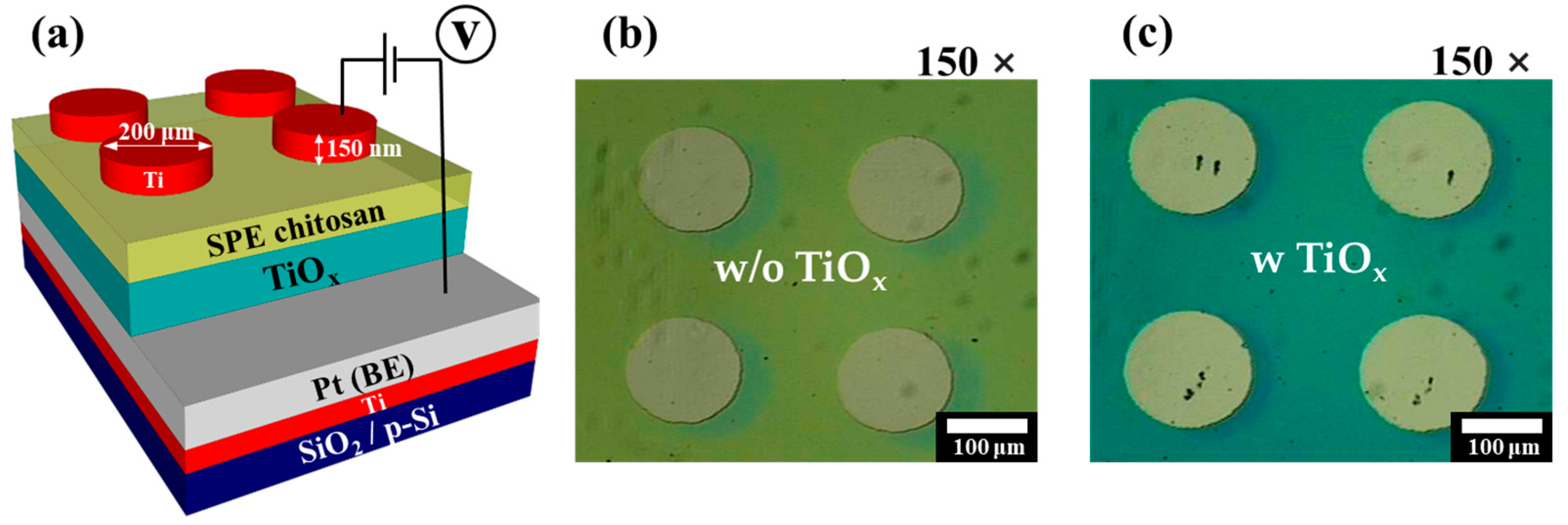
We fabricated highly stable SPE–chitosan memristors with an embedded TiOx layer through MW-assisted oxidation. The process started with cleaning the p-type Si wafer ((110) planes silicon wafers) with a 300 nm-thick thermally grown oxide using a standard Radio Corporation of America (New York, NY, USA) cleaning method. To form the bottom electrode (BE) of the memristor with a MIM structure, a 10 nm-thick Ti adhesive layer and a 100 nm-thick Pt layer were sequentially deposited using an electron beam (E-beam) evaporator deposition system. Then, to form the RS layer, a 150 nm-thick Ti layer was deposited using an E-beam evaporator. Subsequently, TiOx was formed with MW-assisted oxidation under the following conditions: rated power, 1800 W for 10 min and ambient O2, MW frequency, 2.45 GHz. The SPE–chitosan solution was spin-coated on the TiOx layer at 6000 rpm for 30 s, dried in ambient air for 24 h, and oven-baked at 80 °C for 10 min. The thickness of the baked chitosan layer was 80 nm. Finally, a 150 nm-thick and 200 μm diameter Ti top electrode (TE) was deposited onto the RS layer using the E-beam evaporator and a shadow mask. The effect of MW-assisted oxidation was verified by fabricating an SPE–chitosan memristor without the TiOx layer. Figure 1a depicts a schematic diagram of the SPE–chitosan memristor with a TiOx layer developed with MW-assisted oxidation, and Figure 1b,c show optical microscopy images of a SPE–chitosan memristor without and with the TiOx layer, respectively, at a magnification of 150×.
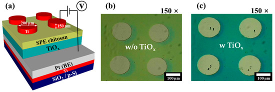
Figure 1.
(a) Schematic diagram of a SPE–chitosan memristor with an embedded TiOx layer developed with MW-assisted oxidation. Optical microscopy images of SPE–chitosan memristor without TiOx (b) and with TiOx (c) at a magnification of 150×.
2.4. Characterization
During measurement, the SPE–chitosan memristors with and without a TiOx layer developed with MW-assisted oxidation were placed on a two-point probe station within a dark shielded box to mitigate electrical noise and external light interference. The RS characteristics and memristive synaptic functions were measured using an Agilent 4156B Precision Semiconductor Parameter Analyzer (Hewlett-Packard Co., Palo Alto, CA, USA). To verify synaptic modulation behavior, electrical pulse stimulations were applied using an Agilent 8110A Pulse Generator (Hewlett-Packard Co.). The fabricated memristors were imaged under an optical microscope using a Sometech SV-55 microscope system (Seoul, Republic of Korea).
3. Results and Discussion
Fourier-transform infrared spectroscopy (FT-IR) was used to analyze the chemical composition of the chitosan electrolyte membrane, an insulating layer, prior to estimating the electrical properties and synaptic operation of the memristors. Figure 2a shows the FT-IR spectrum of the chitosan electrolyte film at wavelengths ranging from 4000 to 900 cm−1, revealing stretching peaks of O-H and C-H around 3350 and 2860 cm−1, respectively. The 1700–1600 cm−1 range was primarily influenced by the amide I region, with the peak at approximately 1640 cm−1 attributed to C=O stretching. The peaks at 1398 and 1101 cm−1 were owing to C-N and C-O stretching, respectively. In general, the spectrum of the chitosan electrolyte film displayed peaks related to amide and -OH groups, which are crucial components of proteins and contribute to the conductivity and mobility of protons [24,25]. Next, we used X-ray photoelectron spectroscopy (XPS) to investigate the Ti2p peak of the embedded TiOx layer. As shown in Figure 2b, the primary peaks in Ti4+ of Ti2p1/2, Ti4+ of Ti2p3/2, and Ti3+ of Ti2p3/2 signals that corresponded with the TiOx component were detected, with binding energies of 464.6, 459.1, and 457.2 eV, respectively. The Ti metallic peak was not observed, indicating nearly complete oxidation of TiOx. In Figure 2c, the O1s peak was deconvoluted using two peaks. The peaks at the binding energies of 529.9 and 530.6 eV may be attributed to oxygen bound to the TiOx layer lattice and oxygen ions near the oxygen vacancy (Vo) in the TiOx layer, respectively. The presence of Vo is a key factor in endowing this material system with RS performance [26,27,28].

Figure 2.
(a) FT-IR spectra of the SPE–chitosan film. XPS peaks of Ti2p (b) and O1s (c) in the TiOx layer developed from MW-assisted oxidation.
Figure 3a,b depict the endurance characteristics of SPE–chitosan memristors prepared without and with TiOx during 100 DC cycles. These characteristics were measured by applying DC bias while grounding the BE. When the TE voltage was applied in the positive direction (as indicated by green arrow 1), the memristor entered the SET (ON) state, indicating a change in resistance from a high-resistance state (HRS) to a low-resistance state (LRS). Conversely, when the voltage was swept in the negative direction (as indicated by green arrow 3), the device changed its resistance state from LRS to HRS, resulting in a RESET (OFF) operation. Thus, both SPE–chitosan memristors exhibited typical BRS properties. The contact between the electrode and the chitosan electrolyte can be utilized for cation-based electrochemical conversion owing to the redox reaction of mobile ions in the polymer electrolyte [6,29]. The electrochemical metallization reaction significantly affects the RS operation when an electric field is applied to the electrode of the chitosan–TiOx nanocomposite film. Metal electrodes that are reactive to electrochemistry supply and discharge mobility cations allow the development of highly conductive filaments [30]. The HRS and LRS were extracted from repetitive BRS I–V curves at a read voltage of 0.1 V, as shown in Figure 3c,d. For the SPE–chitosan memristor without TiOx, the average resistance values of the HRS and LRS were 1.03 × 10³ Ω and 1.55 × 10² Ω, respectively, with standard deviations (SDs) of 7.24 × 101 Ω and 8.15 Ω. In contrast, the average resistance values of the HRS and LRS for the SPE–chitosan memristor with embedded TiOx were 2.42 × 10³ Ω and 1.43 × 10² Ω, respectively, with SDs of 1.06 × 10² Ω and 6.71 Ω. This indicates that the SPE–chitosan memristor with TiOx has a larger RS memory window and lower SD than the one without TiOx. Furthermore, the RS window, defined as the minimum HRS/maximum LRS, increased from 4.1 to 12.0 due to the embedded TiOx. This can be attributed to the abundant oxygen lattice and ions in TiOx, leading to a stable RS operation and higher HRS, resulting in a larger memory window [31].
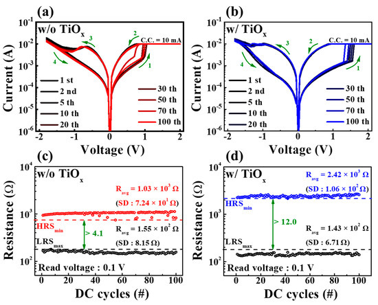
Figure 3.
RS endurance characteristics during 100 DC cycles. BRS I–V curves of SPE–chitosan memristors without (a) and with (b) TiOx. Resistance values of SPE–chitosan memristors without (c) and with (d) TiOx.
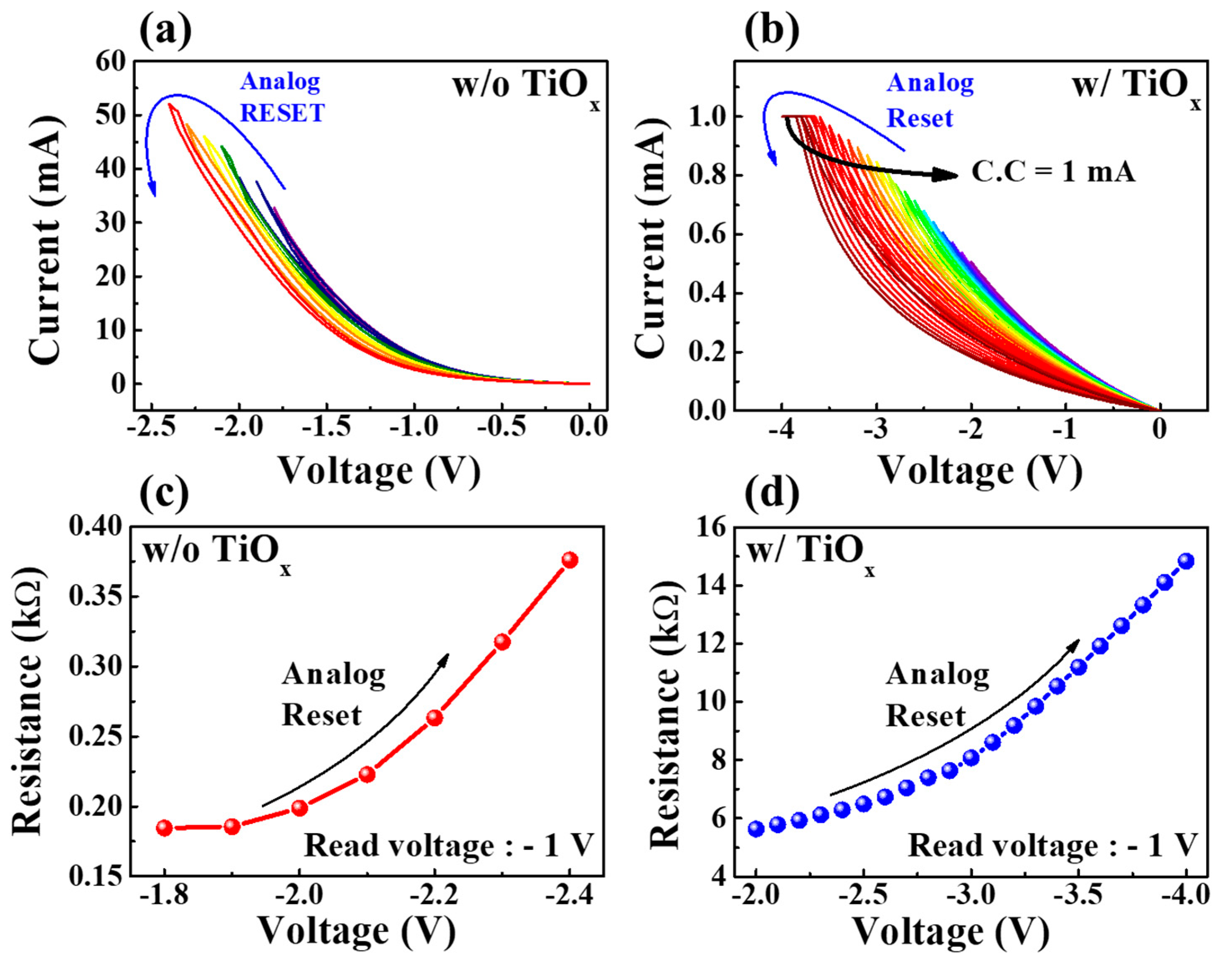
Modulating multi-step conduction is a key factor in achieving high-density memory storage for synaptic devices. Figure 4a,b demonstrate the analog RESET process of SPE–chitosan nanocomposite memristors without and with TiOx, respectively. The SPE–chitosan memristor without TiOx exhibited seven analog RESET states with a gradually decreasing range of the maximum negative RESET voltage between −1.8 and −2.4 V with an interval of −0.1 V after a single positive digital SET operation. In contrast, the SPE–chitosan memristor with TiOx had 21 analog RESET states with a compliance current of 1 mA, and a RESET voltage range of −2 to −4 V with an interval of −0.1 V after one positive digital SET operation. The storage capacity corresponding to the memory window of the memristor depends on the size of the Ion/Ioff changes. The results shown in Figure 4a,b demonstrate that our approach significantly increases the storage capacity density of a memristor device. Figure 4c,d depict the resistance change in each device, extracted at a read voltage of −1 V. Notably, the SPE–chitosan memristor with TiOx exhibited a significantly higher resistance change value (∆9.20 kΩ) than the SPE–chitosan memristor without TiOx (∆0.19 kΩ), indicating more stable and reliable memristive operation. Moreover, the SPE–chitosan–TiOx nanocomposite memristor displayed multi-level changes in resistance, allowing for the representation of multi-level weight changes in synapses. These findings suggest that the SPE–chitosan–TiOx nanocomposite memristor holds great potential for both memristive switching operation and artificial synaptic function [32].

Figure 4.
Analog RESET process for SPE–chitosan memristors without (a) and with (b) TiOx. Graphs (c,d) show the corresponding resistances extracted at a read voltage of −1 V.
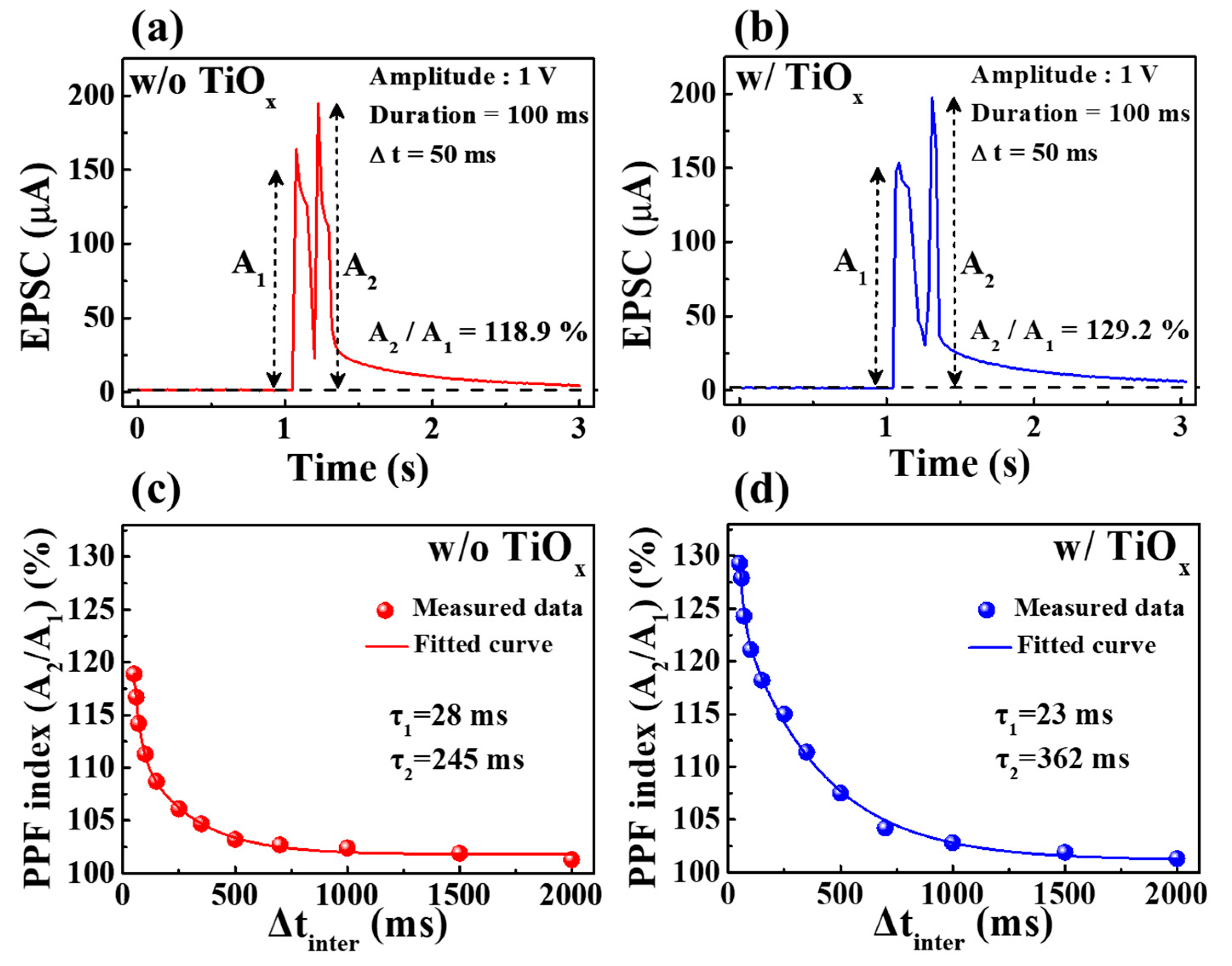
Neural facilitation, which is a dynamic increase in a transporter level and the decoding of biological information, such as visual or auditory data, is an important concept in biological neuroscience. PPF is a typical property of short-term synaptic plasticity and a form of neural facilitation, whereby the second pre-synaptic spike amplifies the first post-synaptic spike. Depending on the time interval (∆tinter) between two successive pre-synaptic spikes, the second synaptic spike causes a larger excitatory post-synaptic current (EPSC) for PPF. The proton transfer ions moved by the first spike accumulate between the electrolyte and the interface. At short ∆tinter, mobile protons accumulate continuously at the interface because they have insufficient time to return to their initial position [33,34]. Figure 5a,b depict the EPSC responses triggered by paired pre-synaptic spikes with an amplitude of 1 V and a duration of 100 ms applied at 50 ms intervals of SPE–chitosan memristors without and with TiOx, respectively. Both memristors showed a higher response in the second EPSC (A2) than in the first (A1), with the SPE–chitosan memristor with TiOx exhibiting a larger EPSC than the one without. The PPF index, calculated as the ratio of the EPSC peak amplitudes (A2/A1), is shown in Figure 5c,d as a function of ∆tinter. The PPF index increases for short ∆tinter and decreases for long ∆tinter, mimicking a biological synaptic response [35]. Notably, the SPE–chitosan memristor with TiOx had a higher PPF index value (~129.2%) than the one without (~118.9%). The PPF index values were fitted using a double-exponential decay function [36]:
where A is a constant fixed value, C1 and C2 indicate the initial facilitation magnitude values, and τ1 and τ2 represent typical relaxation times, respectively. The exponential decay process of PPF can be well modeled by a double exponential decay relation, as shown by the solid lines in Figure 5c,d [37]. For the SPE–chitosan memristor without TiOx, the values of τ1 and τ2 were 28 ms and 245 ms, respectively, whereas for the memristor with TiOx, the values were 23 ms and 362 ms, respectively. These values are in good agreement with those observed in biological synapses and demonstrate that the proposed devices can mimic the fast and slow timescales of synaptic events, which occur on the order of tens and hundreds of milliseconds, respectively [38].
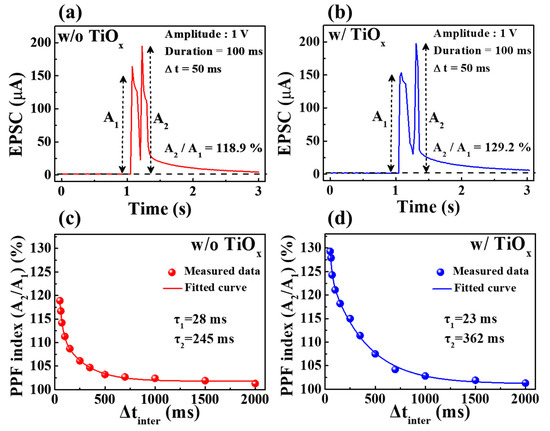
Figure 5.
EPSCs triggered by paired presynaptic spikes in SPE–chitosan memristors without (a) and with (b) TiOx. PPF index values of SPE–chitosan memristors without (c) and with (d) TiOx.
The short-term plasticity of synapses is temporary, whereas long-term plasticity allows for memory through changes in the synaptic weights. STDP is a crucial mechanism for memory and learning in biological neural networks and is determined by the temporal sequence of activity between pre- and post-synaptic neurons. STDP improves on Hebbian learning rules, which regulate neural connection strength, through temporal correlation neural learning. Its simplicity, biological relevance, and computational capabilities in neuroscience make STDP highly interesting [39,40]. Long-term potentiation (LTP) and long-term depression (LTD) in the proposed memristors are determined by STDP and characterized by a constant increase and sustained weakening of synaptic weight, respectively. Figure 6 illustrates the STDP features in the excitatory response mode, wherein the synaptic weight (ΔT = tpost − tpre) for precise time differences is influenced by the pre-synaptic arrival time (tpre) and the post-synaptic production time (tpost). The synaptic weight change (ΔW) is plotted as dots, showing asymmetric Hebbian learning STDP properties, which resemble biological STDP functions. When the post-synaptic spike follows the pre-synaptic spike (ΔT > 0), long-term potentiation occurs due to the strengthening of the synaptic weights, resulting from a decrease in |∆T|. Conversely, when the post-synaptic spike precedes the pre-synaptic spike (ΔT < 0), long-term depression properties occur due to a weakening of the synaptic weights. Additionally, as |∆T| increases, the synaptic weight change decreases. In the inverted STDP mode, the SPE–chitosan memristor’s response mode becomes inhibitory. The STDP learning function can be defined using the following equation [41,42]:
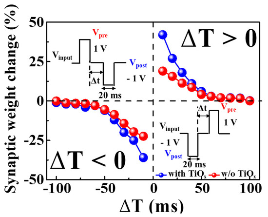
Figure 6.
STDP characteristics of excitatory response modes of SPE–chitosan memristors with and without TiOx. Insets represent timing differences between pre-synaptic and post-synaptic signals through a series of spikes.
The time constant τ± represents the range of ∆T within which synaptic connections can be either strengthened or weakened. When ΔT approaches zero, the maximal synaptic weight change is determined by A+. Consequently, the synaptic weight change values (in percentage) of SPE–chitosan memristors with TiOx exceed those of memristors without TiOx. These findings suggest that SPE–chitosan memristors with TiOx more accurately emulate the biological STDP operation than those without TiOx [43].
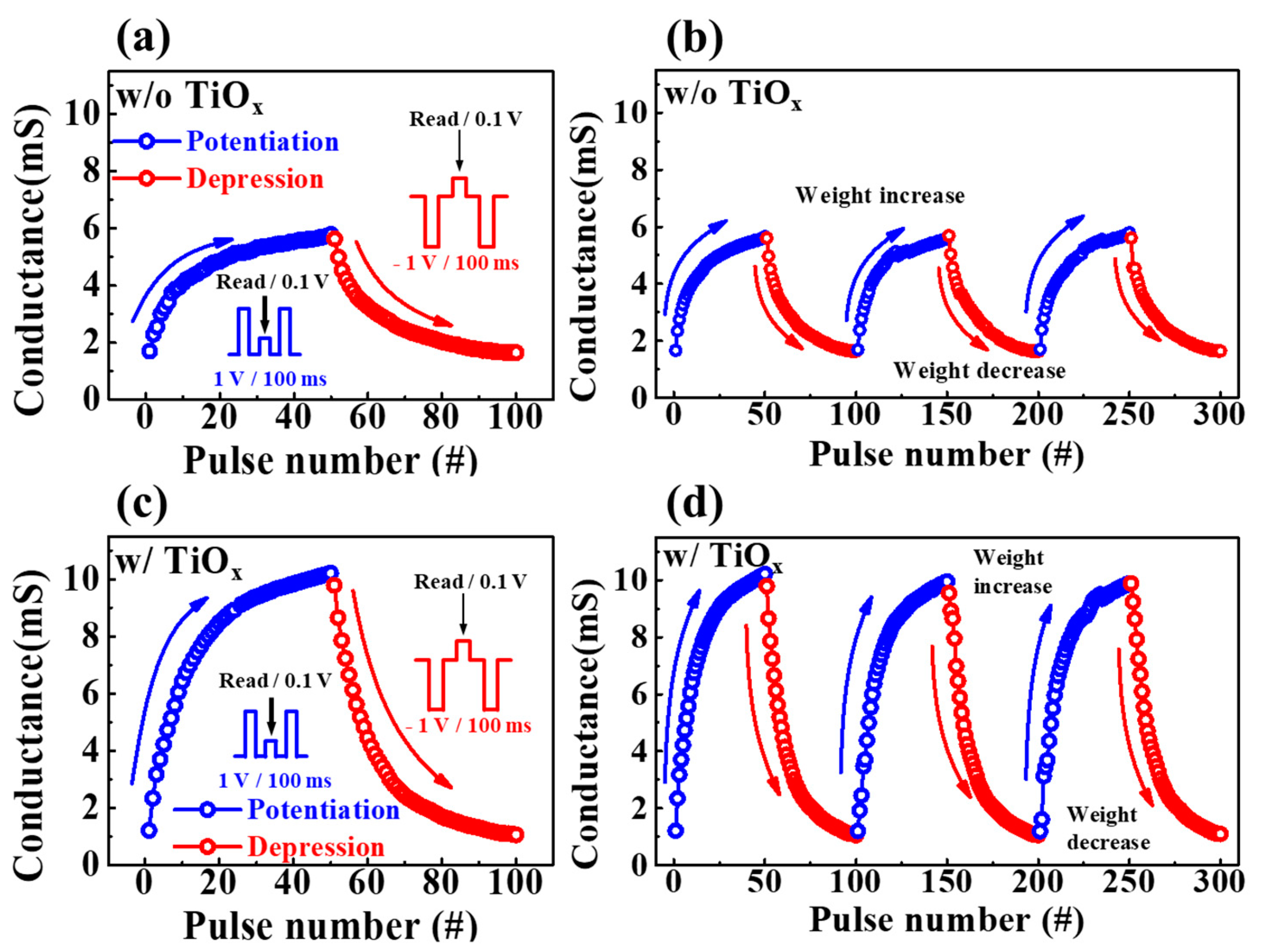
To investigate the gradual modulation of conductivity corresponding to crucial electrical pulse stimulation for memristive switching, the changes in synaptic weight during potentiation and depression were examined. Figure 7a,c illustrate the characteristics of conductance modulation in response to repetitive pre-synaptic spikes. One cycle of 50 potentiation pulses (1 V/100 ms) and 50 depression pulses (−1 V/100 ms) clearly induced conductivity changes. The inset schematics represent a single pre-spike indicating potentiation and depression read pulses. Figure 7c shows that the dynamic range of conductance modulation for SPE–chitosan memristors with TiOx was approximately 9.7 mS, whereas, for memristors without TiOx, it was approximately 5.6 mS, as shown in Figure 7a. The endurance properties for potentiation and depression over three cycles, which indicate the reliability of weight modulation, are depicted in Figure 7b,d. The results demonstrate that SPE–chitosan memristors with TiOx maintain stable operation with a wide conductance dynamic range during cycle repetition, whereas memristors without TiOx exhibit small changes in conductance. Therefore, the proposed SPE–chitosan memristor with TiOx is more effective in improving memory function and achieving uniform weight modulation in response to potentiation and depression pulses. Moreover, the high conductivity of the artificial synaptic device suggests its potential for enhanced learning effects, further validating its feasibility for practical applications [44,45,46].

Figure 7.
One cycle of 50 potentiation pulses and 50 depression pulses in SPE–chitosan memristors without (a) and with (c) TiOx. Three consecutive cycles of conductance modulation operations were successively performed by applying 300 pulses on SPE–chitosan memristors without (b) and with (d) TiOx.
All conductivity values were normalized to the maximum conductivity (G/Gmax) shown in Figure 7a,c. We determined the dynamic range (DR), asymmetric ratio (AR), and linearity, which are highly correlated with learning and recognition simulation, by examining the nonlinearity of the normalized conductance. The DR (Gmax/Gmin) of the SPE–chitosan memristor with TiOx was 9.64, and the DR of the SPE–chitosan memristor without TiOx was 3.5, which was 2.75 times that of the memristors without TiOx. Higher DR values indicate improved precision and recognition performance [47]. The AR represents the asymmetry of changes in conductance potentiation and depression. To evaluate the asymmetry of changes in conductance potentiation and depression, we calculated the AR using Equation (3), where Gp(n) and Gd(n) denote the conductance values during the nth pulse of potentiation and depression, respectively [48]. The AR is a key parameter that can provide insights into the learning and recognition performance of neuromorphic computing systems and can aid in optimizing the design of artificial synapses:
An AR value closer to 0 indicates a more symmetrical conductivity change, which can lead to optimal learning performance. The AR values for the SPE–chitosan memristors with and without TiOx were 0.7 and 0.72, respectively. The value of the device with TiOx was closer to 0, indicating a more symmetrical conductivity change. Furthermore, the linearity of the conductivity was confirmed by extracting the nonlinearity factor using Equation (4) [49]:
where Gmax and Gmin indicate the maximum and minimum conductivity, respectively, and w is an internal variable between 0 and 1. The nonlinearity factor, denoted as α, controls potentiation (αp) or depression (αd), with an ideal value of 1. The αp and αd values for the SPE–chitosan memristors with and without embedded TiOx were 2.91 and −0.9, respectively, indicating a higher linearity in the conductivity increase and decrease in the memristors with TiOx than in that without TiOx (αp = 4.85, αd = −2.12). The SPE–chitosan memristor with embedded TiOx allows for an efficient control of the conductivity through lower amplitudes and fewer pulse numbers. Therefore, the proposed device enables low-power and high-speed operation and is expected to achieve a more efficient learning effect. Consequently, the SPE–chitosan memristor with embedded TiOx is expected to demonstrate great potential as an artificial synapse for data processing compared to the memristor without TiOx.
4. Conclusions
We developed a high-performance organic–inorganic hybrid memristor with embedded TiOx, which was formed by applying low-thermal-budget MW-assisted oxidation to an SPE–chitosan layer. Two types of memristors, with and without the TiOx layer, were prepared to examine the effect of this layer on the organic–inorganic hybrid memristor synaptic device properties. We characterized their resistive and memristive switching properties, as well as various biological synapse functions. Both devices exhibited BRS behavior, endurance, and consistent resistance distribution over 100 DC cycles. However, the device with the TiOx layer demonstrated a larger memory window owing to the formation of highly conductive filaments at the interface with the chitosan layer through metal ion adsorption. Furthermore, the SPE–chitosan memristor with TiOx demonstrated improved memristive switching operation, effectively emulating short- and long-term synaptic plasticity through phenomena such as PPF, STDP, and potentiation properties. These improvements were attributed to the larger change in synaptic weights than in the device without TiOx. In conclusion, the SPE–chitosan memristor with an embedded TiOx layer, which effectively mimics biological artificial synapses, holds great promise for biocompatible and environmentally friendly neuromorphic systems.
Author Contributions
Conceptualization, D.-H.L. and W.-J.C.; investigation, D.-H.L. and W.-J.C.; writing—original draft preparation, D.-H.L. and W.-J.C.; writing—review and edition, D.-H.L., H.P., and W.-J.C.; supervision, W.-J.C.; project administration, W.-J.C.; funding acquisition, W.-J.C. All authors have read and agreed to the published version of the manuscript.
Funding
This work was supported by the Korea Institute for Advancement of Technology (KIAT) grant funded by the Korean government (MOTIE) (P0020967, The Competency Development Program for Industry Specialist).
Institutional Review Board Statement
Not applicable.
Informed Consent Statement
Not applicable.
Data Availability Statement
Not applicable.
Acknowledgments
This study was funded by a research grant of Kwangwoon University in 2023 and the Excellent Research Support Project of Kwangwoon University in 2023. The work reported in this paper was conducted during the sabbatical year of Kwangwoon University in 2023.
Conflicts of Interest
The authors declare no conflict of interest.
Sample Availability
Not applicable.
References
- Zanotti, T.; Puglisi, F.M.; Pavan, P. Smart logic-in-memory architecture for low-power non-von Neumann computing. IEEE J. Electron Devices Soc. 2020, 8, 757–764. [Google Scholar] [CrossRef]
- Indiveri, G.; Liu, S.C. Memory and information processing in neuromorphic systems. Proc. IEEE 2015, 103, 1379–1397. [Google Scholar] [CrossRef]
- Khalid, M. Review on various memristor models, characteristics, potential applications, and future works. Trans. Electr. Electron. Mater. 2019, 20, 289–298. [Google Scholar] [CrossRef]
- Yanagida, T.; Nagashima, K.; Oka, K.; Kanai, M.; Klamchuen, A.; Park, B.H.; Kawai, T. Scaling effect on unipolar and bipolar resistive switching of metal oxides. Sci. Rep. 2013, 3, 1657. [Google Scholar] [CrossRef] [PubMed]
- Rodgers, P. (Ed.) Nanoscience and Technology: A Collection of Reviews from Nature Journals; Nature Publishing Group: New York, NY, USA, 2009. [Google Scholar]
- Raeis-Hosseini, N.; Lee, J.S. Resistive switching memory using biomaterials. J. Electroceram. 2017, 39, 223–238. [Google Scholar] [CrossRef]
- Wang, Z.; Joshi, S.; Savel’ev, S.E.; Jiang, H.; Midya, R.; Lin, P.; Hu, M.; Ge, N.; Strachan, J.P.; Li, Z.; et al. Memristors with diffusive dynamics as synaptic emulators for neuromorphic computing. Nat. Mater. 2017, 16, 101–108. [Google Scholar] [CrossRef]
- Min, S.Y.; Cho, W.J. Memristive switching characteristics in biomaterial chitosan-based solid polymer electrolyte for artificial synapse. Int. J. Mol. Sci. 2021, 22, 773. [Google Scholar] [CrossRef] [PubMed]
- Zhou, G.; Ren, Z.; Wang, L.; Sun, B.; Duan, S.; Song, Q. Artificial and wearable albumen protein memristor arrays with integrated memory logic gate functionality. Mater. Horiz. 2019, 6, 1877–1882. [Google Scholar] [CrossRef]
- Hussain, T.; Abbas, H.; Youn, C.; Lee, H.; Boynazarov, T.; Ku, B.; Jeon, Y.R.; Han, H.; Lee, J.H.; Choi, C.; et al. Cellulose nanocrystal based bio-memristor as a green artificial synaptic device for neuromorphic computing applications. Adv. Mater. Technol. 2022, 7, 2100744. [Google Scholar] [CrossRef]
- Kim, D.H.; Viventi, J.; Amsden, J.J.; Xiao, J.; Vigeland, L.; Kim, Y.S.; Blanco, J.A.; Panilaitis, B.; Frechette, E.S.; Contreras, D.; et al. Dissolvable films of silk fibroin for ultrathin conformal bio-integrated electronics. Nat. Mater. 2010, 9, 511–517. [Google Scholar] [CrossRef]
- Madera-Santana, T.J.; Herrera-Méndez, C.H.; Rodríguez-Núñez, J.R. An overview of the chemical modifications of chitosan and their advantages. Green Mater. 2018, 6, 131–142. [Google Scholar] [CrossRef]
- Wu, G.; Zhang, J.; Wan, X.; Yang, Y.; Jiang, S. Chitosan-based biopolysaccharide proton conductors for synaptic transistors on paper substrates. J. Mater. Chem. C 2014, 2, 6249–6255. [Google Scholar] [CrossRef]
- Hosseini, N.R.; Lee, J.S. Biocompatible and flexible chitosan-based resistive switching memory with magnesium electrodes. Adv. Funct. Mater. 2015, 25, 5586–5592. [Google Scholar] [CrossRef]
- Rehman, M.M.; Siddiqui, G.U.; Gul, J.Z.; Kim, S.W.; Lim, J.H.; Choi, K.H. Resistive switching in all-printed, flexible and hybrid MoS2-PVA nanocomposite based memristive device fabricated by reverse offset. Sci. Rep. 2016, 6, 36195. [Google Scholar] [CrossRef] [PubMed]
- Jefferson, M.T.; Rutter, C.; Fraine, K.; Borges, G.V.; de Souza Santos, G.M.; Schoene, F.A.; Hurst, G.A. Valorization of sour milk to form bioplastics: Friend or foe? J. Chem. Educ. 2020, 97, 1073–1076. [Google Scholar] [CrossRef]
- Gedye, R.; Smith, F.; Westaway, K.; Ali, H.; Baldisera, L.; Laberge, L.; Rousell, J. The use of microwave ovens for rapid organic synthesis. Tetrahedron Lett. 1986, 27, 279–282. [Google Scholar] [CrossRef]
- Surati, M.A.; Jauhari, S.; Desai, K.R. A brief review: Microwave assisted organic reaction. Arch. Appl. Sci. Res. 2012, 4, 645–661. [Google Scholar]
- Ge, H.C.; Luo, D.K. Preparation of carboxymethyl chitosan in aqueous solution under microwave irradiation. Carbohydr. Res. 2005, 340, 1351–1356. [Google Scholar] [CrossRef]
- Bassyouni, F.A.; Abu-Bakr, S.M.; Rehim, M.A. Evolution of microwave irradiation and its application in green chemistry and biosciences. Res. Chem. Intermed. 2012, 38, 283–322. [Google Scholar] [CrossRef]
- Yu, H.P.; Zhu, Y.J.; Lu, B.Q. Highly efficient and environmentally friendly microwave-assisted hydrothermal rapid synthesis of ultralong hydroxyapatite nanowires. Ceram. Int. 2018, 44, 12352–12356. [Google Scholar] [CrossRef]
- Akbarian-Tefaghi, S.; Wiley, J.B. Microwave-assisted routes for rapid and efficient modification of layered perovskites. Dalton Trans. 2018, 47, 2917–2924. [Google Scholar] [CrossRef]
- Dong, C.; Liu, J.; Xing, M.; Zhang, J. Development of titanium oxide-based mesoporous materials in photocatalysis. Res. Chem. Intermed. 2018, 44, 7079–7091. [Google Scholar] [CrossRef]
- Amaral, I.F.; Granja, P.L.; Barbosa, M.A. Chemical modification of chitosan by phosphorylation: An XPS, FT-IR and SEM study. J. Biomater. Sci. Polym. Ed. 2005, 16, 1575–1593. [Google Scholar] [CrossRef]
- Movasaghi, Z.; Rehman, S.; ur Rehman, D.I. Fourier transform infrared (FTIR) spectroscopy of biological tissues. Appl. Spectrosc. Rev. 2008, 43, 134–179. [Google Scholar] [CrossRef]
- Zhao, J.; Zhang, M.; Wan, S.; Yang, Z.; Hwang, C.S. Highly flexible resistive switching memory based on the electronic switching mechanism in the Al/TiO2/Al/polyimide structure. ACS Appl. Mater. Interfaces 2018, 10, 1828–1835. [Google Scholar] [CrossRef] [PubMed]
- Bharti, B.; Kumar, S.; Lee, H.N.; Kumar, R. Formation of oxygen vacancies and Ti3+ state in TiO2 thin film and enhanced optical properties by air plasma treatment. Sci. Rep. 2016, 6, 32355. [Google Scholar] [CrossRef]
- Jackman, M.J.; Thomas, A.G.; Muryn, C. Photoelectron spectroscopy study of stoichiometric and reduced anatase TiO2 (101) surfaces: The effect of subsurface defects on water adsorption at near-ambient pressures. J. Phys. Chem. C 2015, 119, 13682–13690. [Google Scholar] [CrossRef]
- Waser, R.; Dittmann, R.; Staikov, G.; Szot, K. Redox-based resistive switching memories–nanoionic mechanisms, prospects, and challenges. Adv. Mater. 2009, 21, 2632–2663. [Google Scholar] [CrossRef]
- Ambrosi, E.; Bricalli, A.; Laudato, M.; Ielmini, D. Impact of oxide and electrode materials on the switching characteristics of oxide ReRAM devices. Faraday Discuss. 2019, 213, 87–98. [Google Scholar] [CrossRef]
- Peng, W.C.; Chen, Y.C.; He, J.L.; Ou, S.L.; Horng, R.H.; Wuu, D.S. Tunability of p-and n-channel TiOx thin film transistors. Sci. Rep. 2018, 8, 1–11. [Google Scholar] [CrossRef] [PubMed]
- Song, C.; Liu, B.; Wen, W.; Li, H.; Chen, Y. A quantization-aware regularized learning method in multilevel memristor-based neuromorphic computing system. In Proceedings of the IEEE 6th Non-Volatile Memory Systems and Applications Symposium (NVMSA), Hsinchu, Taiwan, 16–18 August 2017; pp. 1–6. [Google Scholar]
- Li, H.K.; Chen, T.P.; Liu, P.; Hu, S.G.; Liu, Y.; Zhang, Q.; Lee, P.S. A light-stimulated synaptic transistor with synaptic plasticity and memory functions based on InGaZnOx–Al2O3 thin film structure. J. Appl. Phys. 2016, 119, 244505. [Google Scholar] [CrossRef]
- Hu, W.; Jiang, J.; Xie, D.; Liu, B.; Yang, J.; He, J. Proton–electron-coupled MoS2 synaptic transistors with a natural renewable biopolymer neurotransmitter for brain-inspired neuromorphic learning. J. Mater. Chem. C 2019, 7, 682–691. [Google Scholar] [CrossRef]
- Guo, L.; Zhang, G.; Han, H.; Hu, Y.; Cheng, G. Light/electric modulated approach for logic functions and artificial synapse behaviors by flexible IGZO TFTs with low power consumption. J. Phys. D Appl. Phys. 2022, 55, 195108. [Google Scholar] [CrossRef]
- Zhao, S.; Ni, Z.; Tan, H.; Wang, Y.; Jin, H.; Nie, T.; Xu, M.; Pi, X.; Yang, D. Electroluminescent synaptic devices with logic functions. Nano Energy 2018, 54, 383–389. [Google Scholar] [CrossRef]
- Zhou, J.; Liu, Y.; Shi, Y.; Wan, Q. Solution-processed chitosan-gated IZO-based transistors for mimicking synaptic plasticity. IEEE Electron Device Lett. 2014, 35, 280–282. [Google Scholar] [CrossRef]
- Zucker, R.S.; Regehr, W.G. Short-term synaptic plasticity. Annu. Rev. Physiol. 2002, 64, 355–405. [Google Scholar] [CrossRef]
- Bliss, T.V.; Lømo, T. Long-lasting potentiation of synaptic transmission in the dentate area of the anaesthetized rabbit following stimulation of the perforant path. J. Physiol. 1973, 232, 331–356. [Google Scholar] [CrossRef]
- Yu, F.; Zhu, L.Q.; Xiao, H.; Gao, W.T.; Guo, Y.B. Restickable oxide neuromorphic transistors with spike-timing-dependent plasticity and Pavlovian associative learning activities. Adv. Funct. Mater. 2018, 28, 1804025. [Google Scholar] [CrossRef]
- Song, S.; Miller, K.D.; Abbott, L.F. Competitive Hebbian learning through spike-timing-dependent synaptic plasticity. Nat. Neurosci. 2000, 3, 919–926. [Google Scholar] [CrossRef]
- Kim, S.; Du, C.; Sheridan, P.; Ma, W.; Choi, S.; Lu, W.D. Experimental demonstration of a second-order memristor and its ability to biorealistically implement synaptic plasticity. Nano Lett. 2015, 15, 2203–2211. [Google Scholar] [CrossRef]
- Markram, H.; Lübke, J.; Frotscher, M.; Sakmann, B. Regulation of synaptic efficacy by coincidence of postsynaptic APs and EPSPs. Science 1997, 275, 213–215. [Google Scholar] [CrossRef] [PubMed]
- Royer, S.; Paré, D. Conservation of total synaptic weight through balanced synaptic depression and potentiation. Nature 2003, 422, 518–522. [Google Scholar] [CrossRef] [PubMed]
- Bliss, T.V.; Cooke, S.F. Long-term potentiation and long-term depression: A clinical perspective. Clinics 2011, 66, 3–17. [Google Scholar] [CrossRef] [PubMed]
- Wang, T.Y.; Meng, J.L.; He, Z.Y.; Chen, L.; Zhu, H.; Sun, Q.Q.; Ding, S.J.; Zhang, D.W. Atomic layer deposited Hf0.5Zr0.5O2-based flexible memristor with short/long-term synaptic plasticity. Nanoscale Res. Lett. 2019, 14, 1–6. [Google Scholar]
- Wang, C.; Li, Y.; Wang, Y.; Xu, X.; Fu, M.; Liu, Y.; Lin, Z.; Ling, H.; Gkoupidenis, P.; Yi, M.; et al. Thin-film transistors for emerging neuromorphic electronics: Fundamentals, materials, and pattern recognition. J. Mater. Chem. C 2021, 9, 11464–11483. [Google Scholar] [CrossRef]
- Yang, C.S.; Shang, D.S.; Liu, N.; Fuller, E.J.; Agrawal, S.; Talin, A.A.; Li, Y.Q.; Shen, B.G.; Sun, Y. All-solid-state synaptic transistor with ultralow conductance for neuromorphic computing. Adv. Funct. Mater. 2018, 28, 1804170. [Google Scholar] [CrossRef]
- Jang, J.W.; Park, S.; Burr, G.W.; Hwang, H.; Jeong, Y.H. Optimization of conductance change in Pr1–xCaxMnO3-based synaptic devices for neuromorphic systems. IEEE Electron Device Lett. 2015, 36, 457–459. [Google Scholar] [CrossRef]
Disclaimer/Publisher’s Note: The statements, opinions and data contained in all publications are solely those of the individual author(s) and contributor(s) and not of MDPI and/or the editor(s). MDPI and/or the editor(s) disclaim responsibility for any injury to people or property resulting from any ideas, methods, instructions or products referred to in the content. |
© 2023 by the authors. Licensee MDPI, Basel, Switzerland. This article is an open access article distributed under the terms and conditions of the Creative Commons Attribution (CC BY) license (https://creativecommons.org/licenses/by/4.0/).

