Article

Nanocrystalline Antiferromagnetic High-κ Dielectric Sr2NiMO6 (M = Te, W) with Double Perovskite Structure Type

1
Department of Chemistry, Josip Juraj Strossmayer Univesity of Osijek, Cara Hadrijana 8/A, HR-31000 Osijek, Croatia
2
Nanomaterials and System Lab, Major of Mechatronics Engineering, Faculty of Applied Energy Systems, Jeju National University, Jeju 63243, Korea
3
Institute of Mathematics, Physics and Mechanics, University of Ljubljana, Jadranska 19, SI-1000 Ljubljana, Slovenia
4
Faculty of Civil and Geodetic Engineering, University of Ljubljana, Jamova 2, SI-1000 Ljubljana, Slovenia
*
Author to whom correspondence should be addressed.
Molecules 2020, 25(17), 3996; https://doi.org/10.3390/molecules25173996
Submission received: 7 August 2020 / Revised: 28 August 2020 / Accepted: 1 September 2020 / Published: 2 September 2020

Abstract

:
Double perovskites have been extensively studied in materials chemistry due to their excellent properties and novel features attributed to the coexistence of ferro/ferri/antiferro-magnetic ground state and semiconductor band gap within the same material. Double perovskites with Sr2NiMO6 (M = Te, W) structure type have been synthesized using simple, non-toxic and costless aqueous citrate sol-gel route. The reaction yielded phase-pure nanocrystalline powders of two compounds: Sr2NiWO6 (SNWO) and Sr2NiTeO6 (SNTO). According to the Rietveld refinement of powder X-ray diffraction data at room temperature, Sr2NiWO6 is tetragonal (I4/m) and Sr2NiTeO6 is monoclinic (C12/m1), with average crystallite sizes of 49 and 77 nm, respectively. Structural studies have been additionally performed by Raman spectroscopy revealing optical phonons typical for vibrations of Te6+/W6+O6 octahedra. Both SNTO and SNWO possess high values of dielectric constants (341 and 308, respectively) with low dielectric loss (0.06 for SNWO) at a frequency of 1 kHz. These values decrease exponentially with the increase of frequency to 1000 kHz, with the dielectric constant being around 260 for both compounds and dielectric loss being 0.01 for SNWO and 0.04 for SNTO. The Nyquist plot for both samples confirms the non-Debye type of relaxation behavior and the dominance of shorter-range movement of charge carriers. Magnetic studies of both compounds revealed antiferromagnetic behavior, with Néel temperature (TN) being 57 K for SNWO and 35 K for SNTO.

1. Introduction

Complex metal oxides have a great fundamental and practical interest. They attract a great attention of the researchers due to the strong correlation between chemical composition, features of the crystal structure, magnetic, electrical and functional properties [1,2,3]. Nanostructured magnetic compounds have been investigated thoroughly as they can possess different physical and chemical properties compared to their bulk counterparts [4,5]. For example, many research groups [6,7,8,9,10,11,12] have shown that the transition temperature in antiferromagnetic materials (TN—Néel temperature) increases with the reduction of particle size. Sometimes, in the case of antiferromagnetic materials, additional transition might be observed [13] or spin canting effect might take place [14,15]. This behavior is usually not reported in bulk forms. Alterations can additionally be observed in dielectric properties and usually they are explained by changes in size, shape and particle or grain boundaries [16,17,18]. Concerning dielectric properties, it is desired to produce a material with high value of dielectric constant (permittivity) and low value of dielectric loss [19,20,21,22]. High-κ dielectric materials are materials with high value of dielectric permittivity. They are used in semiconductor manufacturing processes where they replace widely-used silicon dioxide as gate dielectrics. This allows the increase of the gate performance in term of capacitance [23]. However, most of these materials are manufactured as composites with polymers, such as PVA or PVDF, to increase the value of dielectric constant and decrease the value of dielectric loss [24]. High-κ dielectric polymer composites have been reported to be successful in various applications [25,26,27,28,29,30].
The other thing that can be tailored by particle size control is a value of optical band gap. This has shown a similar trend as transition temperature: It increases with a decrease in particle size [31]. Double perovskite materials are usually reported as semiconductors, with band gap values from 3 to 6 eV [32].
All of the above mentioned properties arise from specific crystal structure and are strongly correlated to it. Perovskite structure is summarized by general formula ABX3, where A is large cation such as alkali or earth alkali, B is small cation mostly transition metal and X stands for oxide, sulfide or halide anion [33]. Multiple substitutions could be performed at either A, B or X sites. In A2B’B’’O6 double perovskites, half of the B site is occupied by one transition metal cation, such as Ni2+ and the other half is occupied by some other transition metal cation, such as W6+ or a semimetal like Te6+ [34]. Here, Ni2+ possess a finite magnetic moment arising from unpaired d electrons, while Te6+ and W6+ are non-magnetic since their d orbitals are empty. This combination might produce some novel effects in single material, which is why these materials have been of a great interest during the last couple of decades.
Sr2NiWO6 (SNWO) and Sr2NiTeO6 (SNTO) have been studied since the 1960s and 1970s of the twentieth century and mostly were prepared in the bulk polycrystalline form or in the form of single crystals. SNWO was previously prepared only once in 2016 in nanocrystalline form using the sol-gel method by Xu et al. [35] and its photocatalytic activity was studied. It was first prepared by Fresia et al. [36] in 1959, then it was studied in the 1960s by Brixner [37], and Nomura [38,39], in the 1970s by Köhl [40] and later by Todate [41], Iwanaga [42], Gateshki [43], Tian [44] and more recently by Liu [45], Blum [46] and Rezaei [47]. SNTO was among first studied by Köhl [48], Lentz [49], Rossman [50] and later studied by Todate [41], Iwanaga [42], Ortega San-Martin [51] and Orayech [52].
Mostly the structure and magnetic properties have been investigated for these compounds with lack of knowledge in the dielectric part. Therefore, in this contribution our goal is to clarify dielectric properties and to investigate the effects that occur due to size reduction to nanoscale. For the first time we give a detailed explanation of dielectric properties for both compounds and show effects of size reduction on the magnetic properties.

2. Results and Discussion

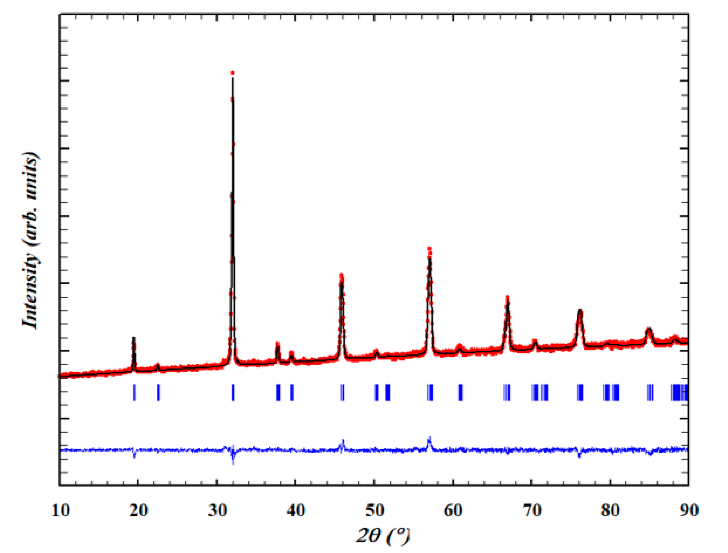
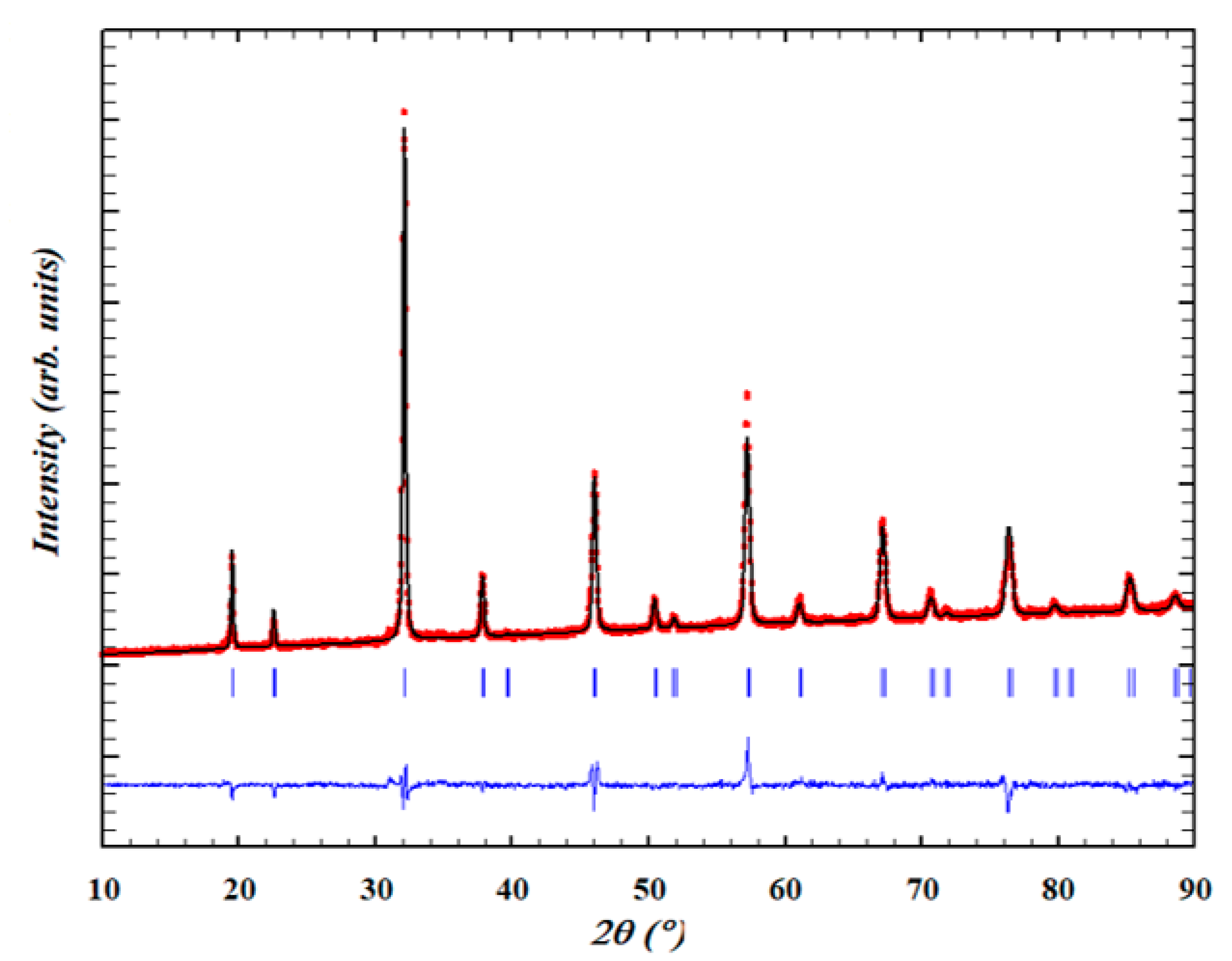
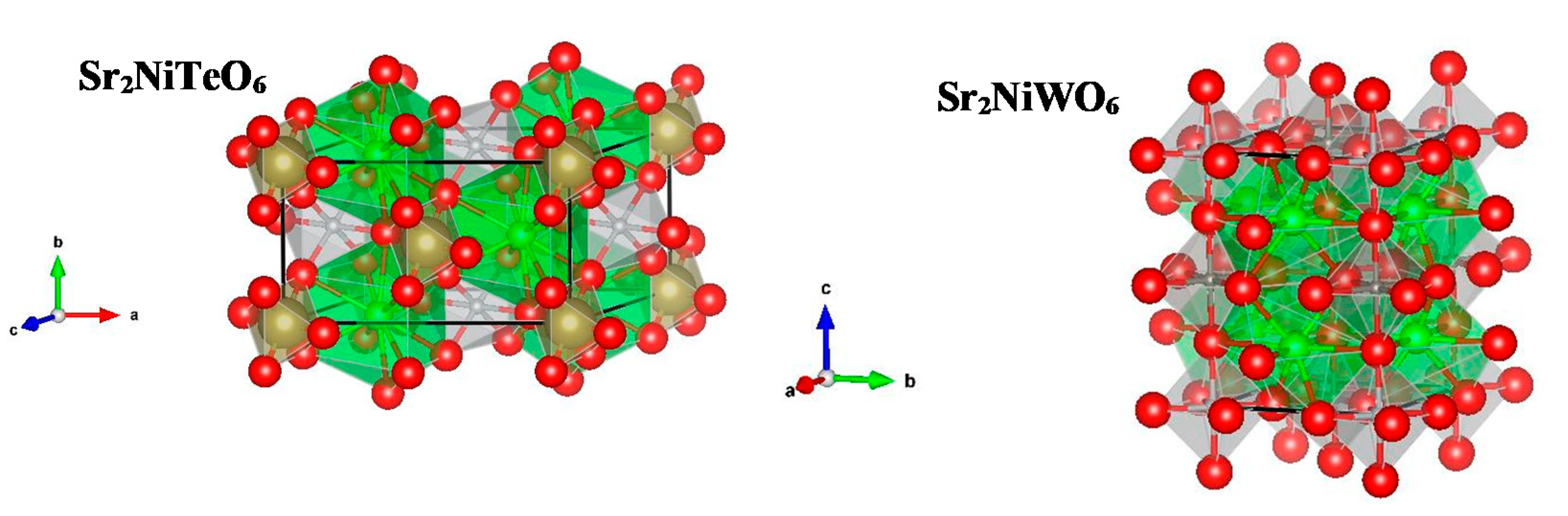
2.1. Powder X-ray Diffraction

Powder X-ray diffraction has been performed in order to investigate phase purity, crystal structure as well as microstructural parameters of as synthesized materials. The Rietveld refinement was conducted along with microstructural analysis [53], and the typical Rietveld output plots are given in Figure 1 and Figure 2 whilst the results of the refinement are summarized in Table 1, Table 2, Table 3 and Table 4. Both figures reveal phase purity of as synthesized double perovskites since all observed Bragg reflections were correctly described by the calculated curve based on the assumed structural models. Only in Figure 2 are several spikes in the difference curve observed; however, they are most probably attributed to some small preferred orientation.
Sr2NiWO6 crystallized in tetragonal centrosymmetric space group I4/m with lattice parameters equal to a = 5.5644(2), c = 7.9025(4) Å, while Sr2NiTeO6 crystallized in monoclinic centrosymmetric space group C12/m1 with lattice parameters: a = 9.663(1), b = 5.6132(2), c = 5.5833(2) Å, β = 125.32(1)°. Although investigated compounds differ significantly in terms of crystal symmetry, their unit cell volume values are quite close.
Comparison of atomic positions extracted by Iwanaga et al. [42] for bulk SNTO with this work, presented in Table 2, reveals quite different values, although they correspond to the same space group. As opposed to nanocrystalline SNTO reported in Table 2, in bulk as reported in [42] there are two different positions for magnetically-active Ni2+ cation (2a and 2d), which could result in different magnetic properties.
Figure 3 shows the crystal structures of as synthesized compounds visualized by VESTA software [54] and Table 4 shows selected interatomic distances calculated by the Rietveld method. SNTO shows structural arrangement consisting of layers of TeO6 octahedra centered in corners of bc planes, mutually linked with NiO6 octahedron, centered in the middle of bc rectangle. The 3D structure was further composed by alternate linking of tilted TeO6-NiO6 octahedra along the [100] direction. The voids formed with such stacking were filled by SrO12 cuboctahedron. SNWO is rock-salt ordered with the arrangements of a mutually slightly-rotated corner-sharing NiO6-WO6 octahedra along the c-axis due to the tetragonal distortion.
In monoclinic Sr2NiTeO6 there are two types of octahedra that differ according to their lengths: shorter (smaller volume) TeO6 octahedra and slightly larger NiO6 octahedra. Moreover, both octahedra are highly distorted since the apical line is not perpendicular to the equatorial plane. Tetragonal Sr2NiWO6 comprises NiO6 octahedra and WO6 octahedra that differ to each other according to their bond lengths: Equatorial bond lengths in NiO6 are visibly shorter compared to WO6, while the apical lengths of NiO6 are slightly longer than in WO6, as seen from the Table 4. It is noteworthy that SrO12 cuboctahedron is more distorted (more different Sn-O bond lengths) for SNTO in comparison with SNWO which is the result of lower symmetry of SNTO. The line broadening analysis performed within the Rietveld refinement reveals that SNTO shows higher crystallinity (average crystallite size equals to 77 nm) compared to SNWO (49 nm). Although the crystallinity is higher for SNTO, its microstrain level is also higher compared to SNWO, which is an unexpected and interesting finding.

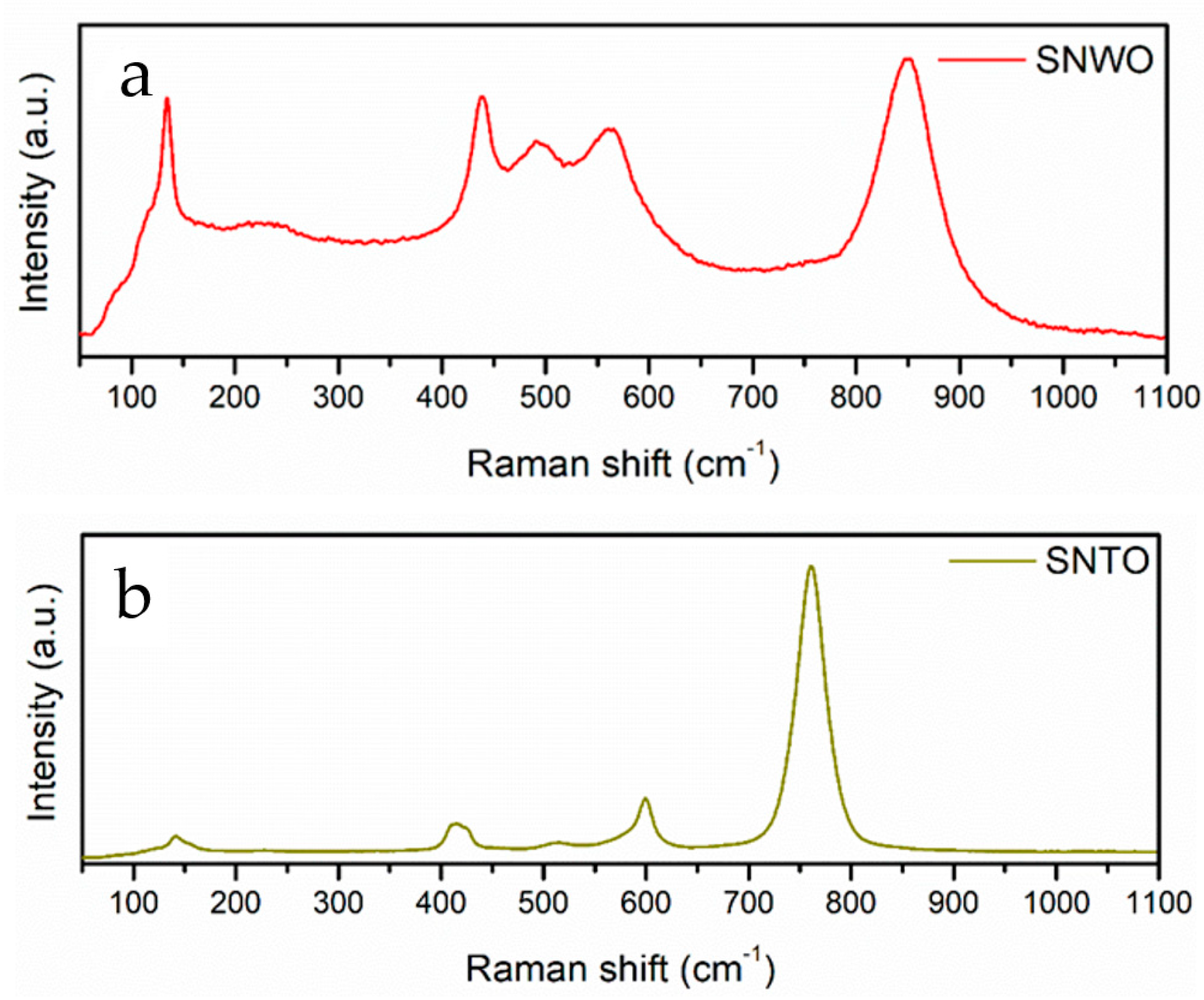
2.2. Unpolarized Raman Spectroscopy

Raman spectroscopy was conducted in order to inspect bond length stretching and possible phonon confinement effects that frequently occur in nanocrystalline materials. Figure 4 shows Raman spectra of double perovskites: tetragonal Sr2NiWO6 (SNWO in Figure 4a), and monoclinic Sr2NiTeO6 (SNTO in Figure 4b). According to Kroumova et al. [55] and based on the space group, Sr2NiTeO6 has 7Ag + 5Bg, 12 first-order Raman active modes (optical modes) in total. Sr2NiWO6 has 3Ag + 3Bg + 31Eg + 32Eg, which is also 12 first-order Raman active modes in total. Only four bands out of 12 for both SNWO and SNTO appear in Figure 4. Peaks appearing in the range from 100–150 cm−1 are assigned to lattice translational modes [51]. They are observed at 134 cm−1 for SNWO and at 142 cm−1 for SNTO. Peaks in the range 350–450 cm−1 are assigned to ν5 mode, which appears due to oxygen bending in octahedra [56,57]. It is observed at 440 cm−1 for SNWO and at 416 cm−1 for SNTO. Since the Te6+-O bond is the shortest bond for the studied SNTO, it is also the strongest bond for this compound and higher frequencies in the spectrum should be primarily assigned to ν1 and ν2 vibrations of the Te6+O6 octahedron. Hence, for SNTO, the frequencies corresponding to vibrations of Ni2+O6 octahedron are not expected and indeed were not observed. Peaks assigned to ν2 mode are due to asymmetric stretching that appear in the range 470–650 cm−1 according to Silva et al. [56]. This mode is represented by two peaks for both compounds, at 497 and 564 cm−1 for SNWO and at 510 and 600 cm−1 for SNTO. The highest wavenumber appearing within spectra (850 cm−1 for SNWO and 762 cm−1 for SNTO) is assigned to ν1, symmetric stretching of the WO6 and TeO6 octahedra, respectively. Optical phonons for both compounds are summarized in Table S1 in the Supporting file. Similar to Silva et al. [56], we also observe a larger difference in the ν1 vibration between Te6+- (d10) and W6+-based (d0) compounds. These authors correlated the increase of wavenumber in W-containing compounds compared to Te-containing compounds with the increase of the force constant (bonding energy) of the W-O bond in the WO6 octahedron. The Te6+ cation has a fully-occupied d10 orbital configuration, which avoids the formation of π-type Te-O bonds. On the other hand, the W6+ cation has a d0 orbital configuration, allowing the overlap of the t2g orbitals The increase of force constant/bonding energy occurs due to the overlapping of t2g orbitals of the octahedrally-coordinated W6+ cation [56]. Similar arguments are valid for the absence of vibrations of Ni2+O6 octahedron for SNWO. Although, the shortest bond in this compound is the equatorial Ni-O bond (1.873(2) Å), the formation of π-type W-O bonds occurred, which resulted in the increase of W-O bonding energy, thus Raman modes of W6+O6 dominate. Ayala et al. [58] studied tetragonal and monoclinic double perovskites and came to conclusion that these spectra resemble to those of cubic Fm-3m perovskites. The similarity comes from the fact that tetragonal and monoclinic structures arise from the small distortions of the cubic cell [56]. When comparing our SNWO spectrum in Figure 7a with the bulk SNWO reported by Manoun et al. [59], there is a progressive shift to lower wavenumbers (lower energies); line shapes are broadened and asymmetric on the lower energy side. Additionally, symmetry breaking becomes more emphasized. These effects occur due to the reduction of size and quantum confinement effect [60,61,62]. Actually, the impact of the size reduction on the Raman spectra is quite visible, since SNWO contains smaller crystals compared to SNTO and thus its Raman bands are also broader, reflecting a higher disorder in SNWO.

2.3. Scanning Electron Microscopy and Energy Dispersive X-ray Spectroscopy

To investigate the morphology and chemical composition of as-prepared compounds, scanning electron microscopy (SEM) and energy dispersive X-Ray spectroscopy (EDX) measurements were performed. SEM images are shown in Figure 5, EDX spectra for both compounds are shown in Figure S1 and Figure S2 in SI.
SEM images show irregularly round-shaped particle agglomerates for both SNTO and SNWO at the same magnification (1 μm). It is clearly visible that SNTO particles are larger than SNWO particles, which is in accordance with microstructural analysis conducted using the Rietveld refinement method. The surface morphology of the particles represents the random distribution of the various size of the grains and visible grain boundaries.
The energy dispersive X-ray spectrum and elemental mapping suggest the presence of all elements is similar to the base composition confirming that both synthesized compounds SNTO and SNWO are free from impurity. Figure S1 shows that Sr2NiWO6 consists of 61.2 at % O, 19.7 at % Sr, 10.8 at % Ni and 8.3 at % W, which nearly corresponds to the proposed chemical formula. It is similar with Sr2NiTeO6, which consists of 63.4 at % O, 18.1 at % Sr, 9.9 at % Ni and 8.6 at % Te (Figure S2).

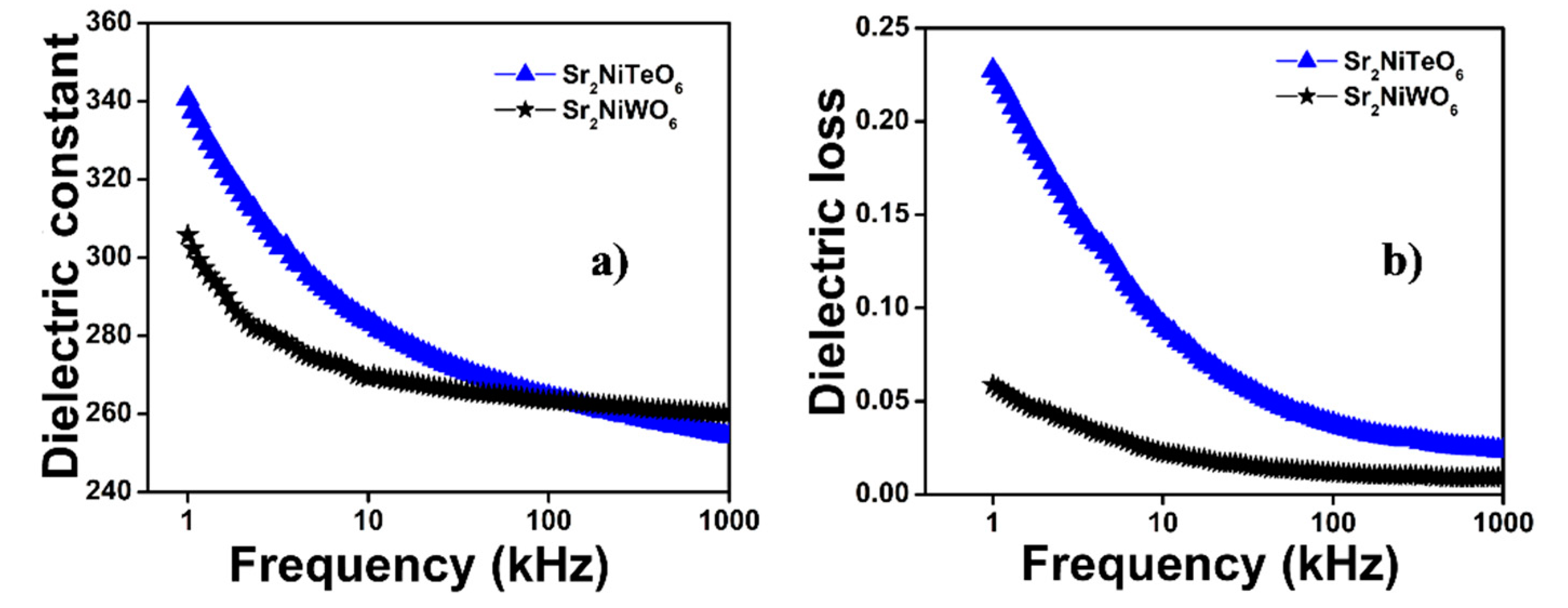
2.4. Dielectric Properties

Figure 6a displays dielectric constant and Figure 6b dielectric loss versus frequency for SNTO and SNWO ceramic samples at room temperature. It is observed that the dielectric constant (εr) and dielectric loss (tan δ) are high at lower frequency regime and decreases at higher frequency regime, indicating that the familiar dielectric dispersion phenomenon as observed in the case of normal ferroelectrics. Frequency-temperature dependence of εr and tan δ is associated with various polarization effects, such as ionic, dipolar, electronic and space charge that appears at multiple levels of material reaction due to short and long-range movement of mobile charges. At low-frequency regions, the space charge and dipolar polarization are at the peak and interfacial polarizations efficiently add to the upper value of εr. In the high-frequency region, the electronic polarizations become most significant compared to other polarizations, leading to invariant dielectric constant. The decrease in the value of dielectric constant with the rise in frequency may be due to the dipoles unable to follow the rapid oscillating field [63]. The dielectric loss has a similar type of trend as εr in the low-frequency regime, where the loss is high due to the influence of compositional disorder, leading to a relaxation phenomenon [64]. Mutual comparison between SNTO and SNWO reveals that SNWO has a lower value of εr (308 compared to 341 at 1 kHz), while its dielectric loss is significantly lower (0.06 compared to 0.23). Moreover, frequency-dependent quantities show milder decrease for SNWO, indicating its better perspective for electronic applications.

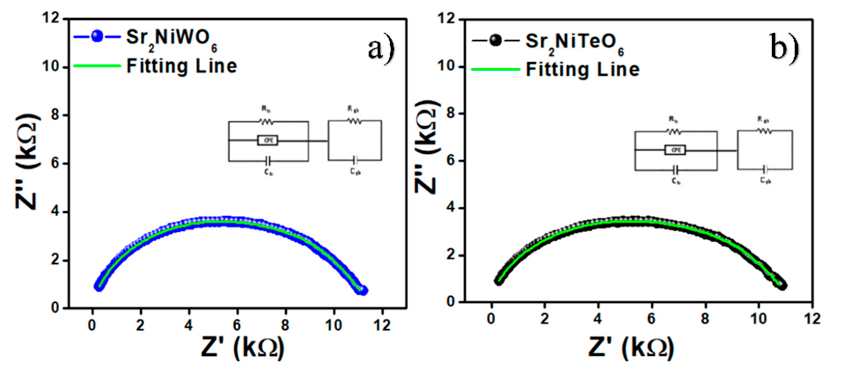
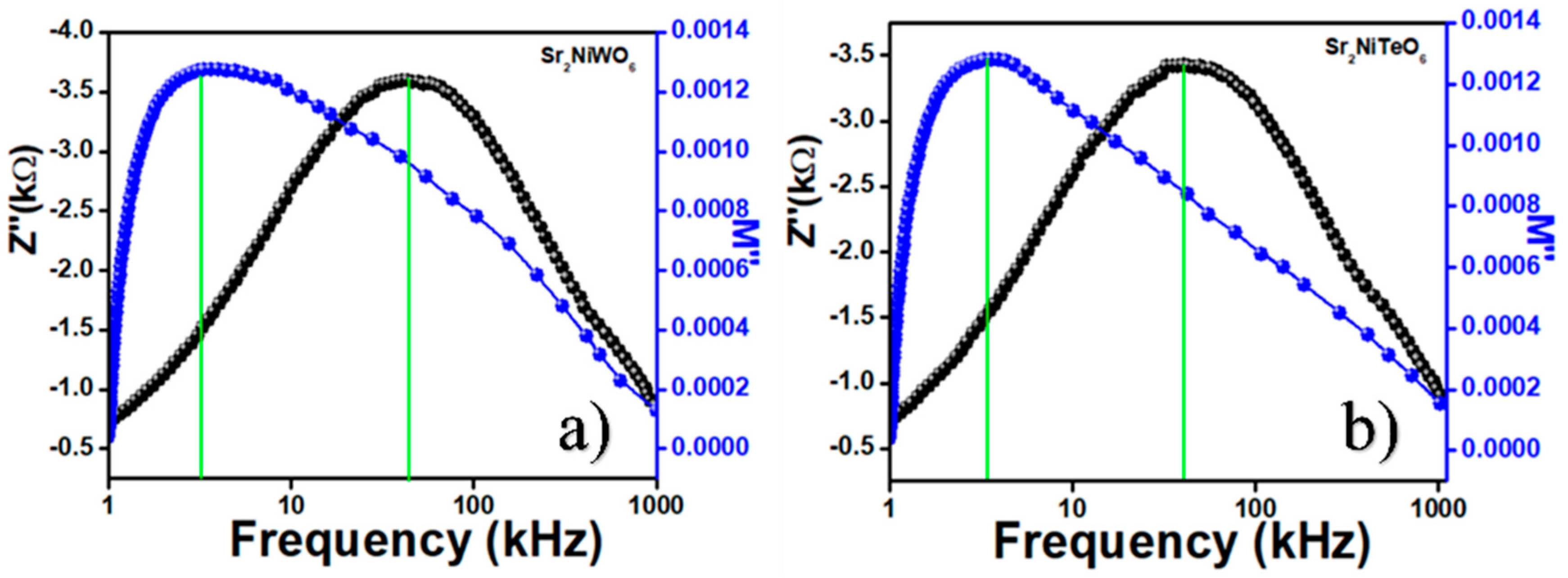
2.5. Impedance Spectroscopy

The Nyquist plot in general has several semicircular arcs, whereby the first circle (higher frequency) represents the grain/bulk effect, the second circle (intermediate frequency) represents the grain boundary effect and the third circle (lower frequency) represents the electrode effect. Normally, depressed semicircular arcs are obtained with the center below the abscissa implying departure from Debye type behavior. There are several factors, such as atomic defect distribution, stress–strain phenomena, grain boundary, and grain orientation, which can be correlated to the above-described non-ideal behavior. The depressed semicircles also provide evidence of polarization phenomena with the allocation of relaxation times. In Debye-type behavior, the center of the circle lies exactly on the real Z-axis [65]. Figure 7 shows the depressed semicircle and the non-Debye type of relaxation phenomena are occurring for both synthesized materials. The commercial Z Smipwin software is used to fit the experimental impedance data to an equivalent circuit model bearing a constant phase element (CPE). The parameters derived from fitting are grain resistance, grain capacitance, grain boundary resistance, and grain boundary capacitance and corresponding values are listed in Table 5. Figure 8 shows the frequency-dependent M′′ and Z′′ plot of (a) SNTO and (b) SNWO ceramics. It represents the effect of longer- and shorter-range movement of charge carriers on the relaxation process. The shorter-range charge carrier dominancy is interpreted by the M′′ and Z′′ peaks mismatch, whereas if the M′′ and Z′′ peaks exactly match then it is related to the long-range motion of charge carriers [66]. In Figure 8a,b, it is depicted that the peaks of the M′′ and Z′′ of SNWO and SNTO coincides in the same position, suggesting the dominance of shorter-range movement of charge carriers.

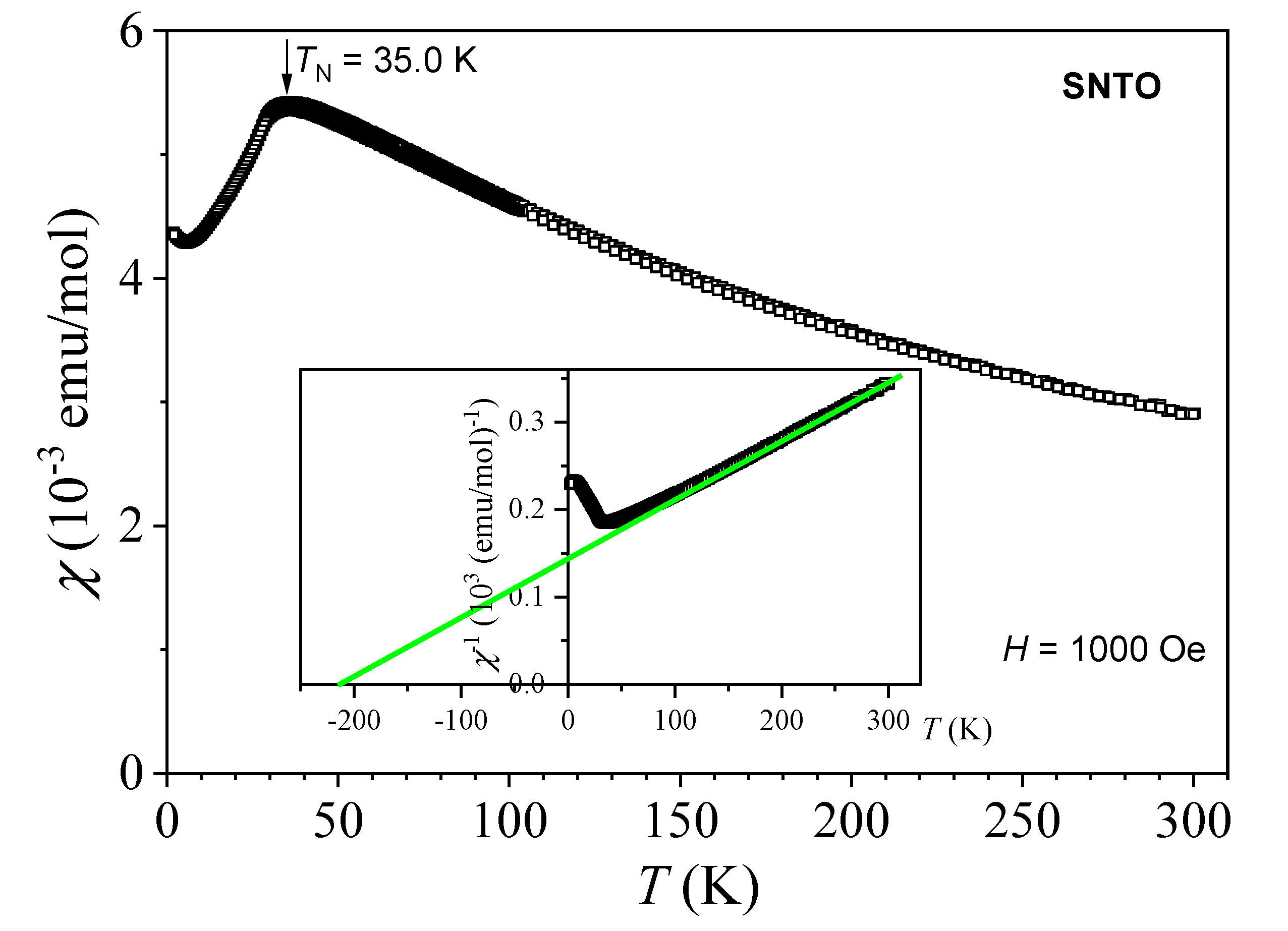
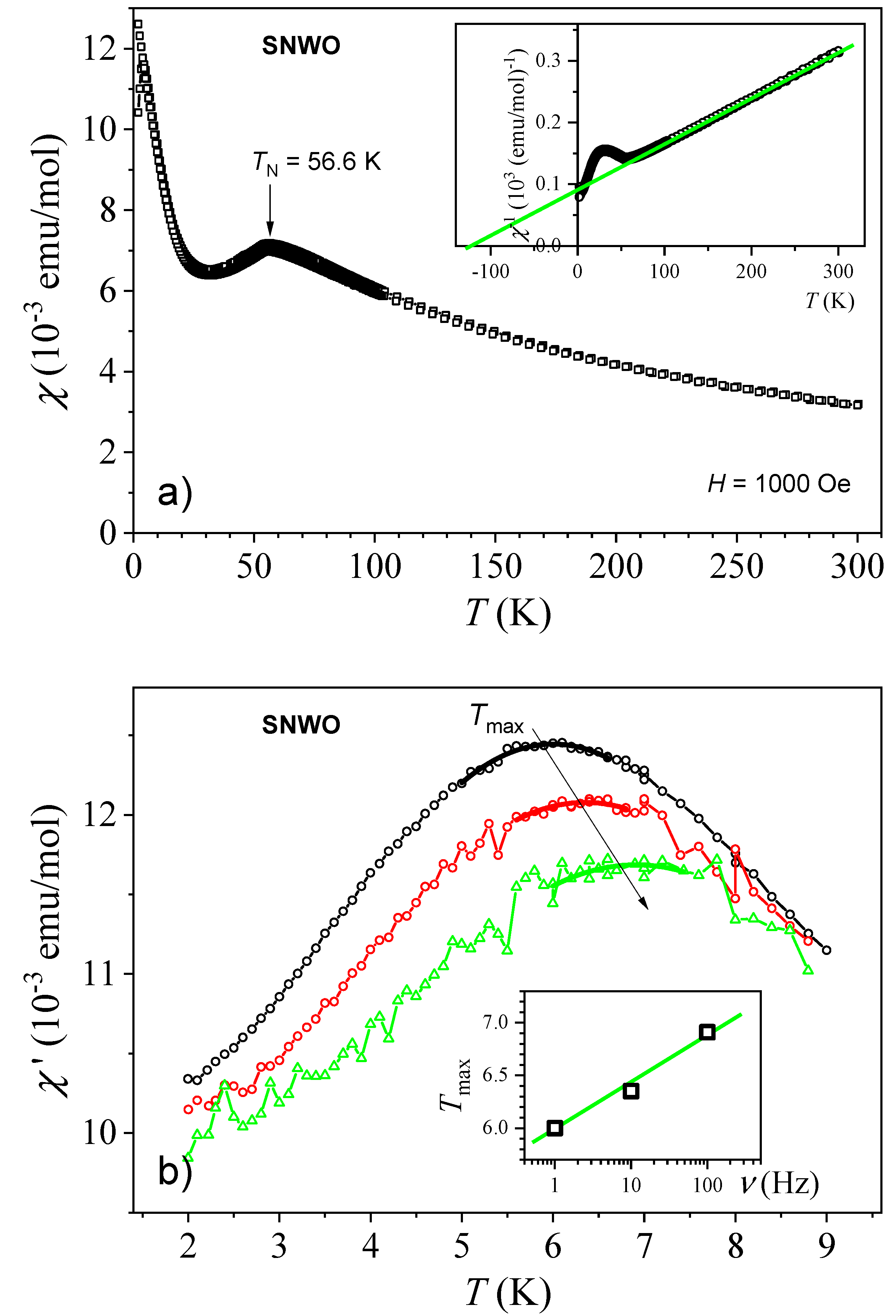
2.6. Magnetic Properties

Temperature-dependent susceptibility of SNTO measured in a magnetic field of 1000 Oe is shown in Figure 9. The susceptibility increases as temperature decreases from room temperature down to 35 K. At Néel temperature (TN) = 35.0 K, the susceptibility exhibits a maximum, in agreement with already reported antiferromagnetic ground state of SNTO [42]. No difference between zero-field-cooled (ZFC) and field-cooled (FC) susceptibility was observed. The measured susceptibility in high temperature region (T > 100 K) was analyzed using a Curie-Weiss law χ = C/(T−ϑ). The result, presented as a full line in χ−1 vs. T plot (inset in Figure 9), gave the Curie constant C = 1.4 emu K/mol and Curie–Weiss temperature ϑ = −210 K. The effective magnetic moment μ   =   8   C = 3.3 μ B in agreement with the expected value for Ni(II) ions with non-zero orbital contribution L [67]. The magnetization curve M(H) at 2 K (Figure S3) is linear up to the maximal magnetic field of 50 kOe with very small magnetization (0.04 μB at 50 kOe), as expected for the antiferromagnetic ground state.
In Figure 10a the temperature-dependent magnetic susceptibility is shown for SNWO. A local maximum of susceptibility (Néel temperature) appears here at a higher Néel temperature (TN) = 56.6 K. The magnetization M(H) curve at 2 K is linear as in SNTO (Figure S3), with a very small value of the magnetization in a maximal field of 50 kOe. Both results speak in favor of antiferromagnetic ground state in SNWO, as already reported in the literature [42,46]. A slightly higher Néel temperature (56.6 K) than the literature data for bulk material (53 K in [42], 54 K in [46]) might be ascribed to a nanosized material in our case. Various researchers have already described that Néel temperature increases with the decrease in crystallite size [6,7,8,9,10,11,12].
Above TN, the susceptibility follows the Curie–Weiss law (inset in Figure 10). The same analyses as performed in the case of SNTO (Curie-Weiss fit), which gave the Curie–Weiss temperature ϑ = −125 K and effective magnetic moment of 3.2 μB. These values are similar to the literature data [42,46].
However, below TN, the susceptibility starts to increase once again. The ZFC/FC splitting can be observed below 6 K, which was, to our knowledge, not reported yet in literature. In order to investigate this low temperature signal in more detail, we performed additional AC susceptibility measurements (susceptibility in alternating magnetic field) shown in Figure 10b. The AC susceptibility has been measured at three different frequencies of the applied magnetic field—1, 10, and 100 Hz. The amplitude of AC magnetic field was 6 Oe. The maximum of AC susceptibility is at approximately Tmax = 6 K for the frequency of the applied field of 1 Hz, and shifts to higher temperatures with frequency. This feature is typical for a frustrated magnetic system, where both ferromagnetic and antiferromagnetic interaction are present in the system simultaneously, and (or) there is some degree of disorder in a distribution of magnetic moments. [68] The relative shift of Tmax with frequency (inset in Figure 10b), Г   =   Δ T max T max ( 1   Hz )   Δ log v = 0.07 , falls somewhere between the values of typical spin glasses and superparamagnetic systems [69]. A very similar signal can be found also in NiO nanoparticles [68]. We tentatively ascribe this low temperature signal to the magnetism of uncompensated nickel ions on the surface of nanoparticles, where the perfect antiferromagnetically-ordered environment around the magnetic ions, as established in bulk compounds, is corrupted.

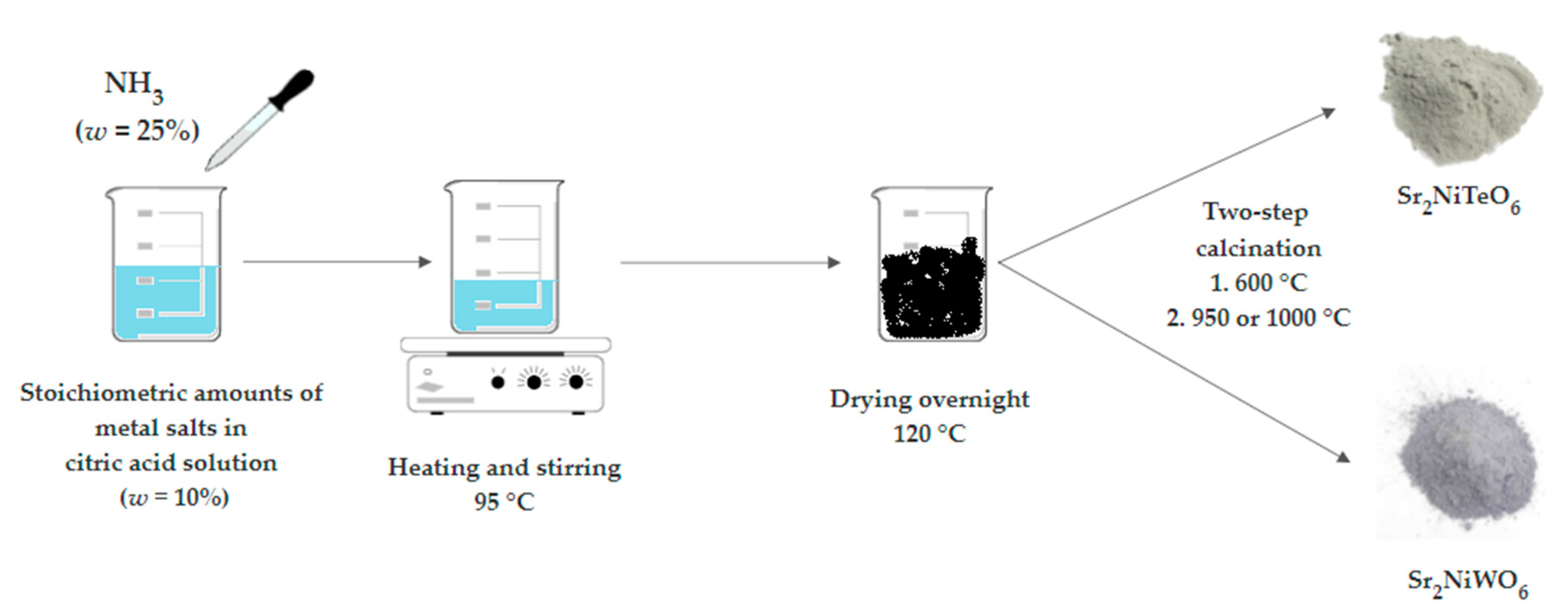
3. Materials and Methods

Materials. The following commercially available chemicals were used without further purification: Ammonium tungsten oxide hydrate and ammonium tellurate from Alfa Aesar, Germany; strontium(II) nitrate, and nickel(II) nitrate hexahydrate from Sigma Aldrich, Germany; citric acid monohydrate 99.9% from T.T.T., Croatia; and concentrated ammonia solution 25% from Gram-Mol, Croatia.
Synthesis. Double perovskites were synthesized using aqueous sol-gel citrate method, previously reported for triple perovskites [57,70]. Stoichiometric amounts were dissolved in 10% citric acid solution (10 g of citric acid in 100 mL of MiliQ water) for synthesis of SNTO: A total of 2 mmol of strontium(II) nitrate, 1 mmol of nickel(II) nitrate hexahydrate and 1 mmol of ammonium tellurate. For synthesis of SNWO, instead of ammonium tellurate, 1/12 mmol of ammonium tungsten oxide (molecular formula: H40N10O41W12•xH2O) was used. The value of pH was adjusted to 5 using concentrated ammonia solution (pH-meter 211, HANNA, Zagreb, Croatia). Reaction mixture was then evaporated at 95 °C, with constant stirring on a magnetic stirrer (IKA RCT Basic, Staufen, Germany), until black resin was formed. Black resin was further dried in a drying oven (Instrumentaria ST-05, Sesvete, Croatia) at 120 °C for 24 h and grinded in a mortar with a pestle. Obtained black powder was first calcined at 600 °C for 8 h and then at 950 °C (SNTO) or 1000 °C (SNWO) for 12 h (Furnace SN 342689, Nabertherm GmbH, Lilienthal, Germany). Heating rate for both calcination steps was 2 °Cper minute. Synthesis procedure is represented in Scheme 1 below.
Preparation of pellets for dielectric measurements. The calcined powder was converted into fine particles and 5 wt % of binder polyvinyl alcohol (PVA) was mixed. Further, disk-shape pellets comprising a diameter of 10 mm and a thickness of 1.2 mm were sieved employing a hydraulic press (Model number: 220-93614-01, Shimadzu, Kyoto, Japan) with cold pressure of 4.0 × 10⁶ Nm−2. Subsequently, the green pellets were sintered at 1250 °C for 4 h at a heating rate of 8 °C/min in a tube furnace (Model number: SH-FU-50TS, SH Scientific, Daejeon, Korea). One of the pellets of each composition was taken and rubbed with zero emery paper to make the opposite sides smooth and parallel. The high-quality silver paint was painted on both opposite sides of each pellet that served as an electrode and further electrical characterization was performed.
Methods. Powder X-Ray diffraction patterns were collected on a Panalytical XPert Pro Diffractometer with θ–2θ geometry (Malvern Panalytical, Malvern, UK), using monochromatized CuKα radiation (40 kV, 40 mA) at 292(2) K, in the range of 2θ from 10°–90° with the step size of 0.02.
Unpolarized Raman spectroscopy was performed at room temperature in backscattering geometry using a Renishaw inVia Raman microscope system (Reinshaw GmbH, Pliezhausen, Germany) with a HeNe laser (633 nm) for excitation, in the range 50–1100 cm−1 with 2 mW laser power. Samples were placed on the microscope slides in a powder form.
The surface morphology was investigated using a scanning electron microscope (M/S TESCAN Mira 3, Brno, Czech Republic).
The resistive and capacitive parameters were fetched from a computer-coupled phase-sensitive meter (Hioki IM3570, Nagano, Japan). The electrical properties of the prepared pellets were examined over a frequency sweep (1 kHz–1 MHz) and at room temperature.
Magnetic properties were investigated using a MPMS-XL-5 magnetometer (Quantum Design, San Diego, CA, USA). All presented data were corrected for diamagnetic contribution estimated from Pascal’s constants [71].

4. Conclusions

This study was performed to clarify the impact of size reduction on magnetic properties and to investigate dielectric properties of synthesized Ni-based double perovskites. Most of the reported literature deal with bulk materials and their magnetic properties along with detailed crystal structure analysis. Since miniaturizing and enhancing the performance has become a trend in the production of electronic devices, our motivation was to decrease crystallite size of already known compounds and to shed some light on their magnetic and electrical properties.
Double perovskites Sr2NiTeO6 and Sr2NiWO6 both possess magnetically active Ni2+ cation and magnetically inactive d10 Te6+ (diameter of 0.56 Å for coordination number 6 [72]) and d0 W6+ (diameter of 0.60 Å for coordination number 6 [72]) cations, respectively. Coexistence of these two species in a single-phase material is one of the conditions for coupling of magnetic and dielectric properties within the same material, which leads to multifunctionality.
So far, we have successfully synthesized, using modified sol-gel route phase pure Ni-based perovskites, Sr2NiTeO6 and Sr2NiWO6. Since the ionic radii values of octahedrally-coordinated Te6+ and W6+ are similar [72], it would be expected that their crystal structures are also similar. The value of their Goldschmidt tolerance factors are the same up to fourth decimal digit (t = 0.9889) [33]. However, even the small difference in ionic radii can produce different structures. Thus, Sr2NiWO6 is crystalized in the tetragonal crystal system (I4/m) with an average crystallite size of 49 nm, while Sr2NiTeO6 is monoclinic (C12/m1) with 77 nm the average crystallite size. On the other hand, monoclinic and tetragonal structures are both formed because of small distortions of the cubic cell, so their similarity is still preserved.
Both compounds are antiferromagnetically ordered, as it has already been reported before for their bulk and single crystal forms. Sr2NiTeO6 behaves the same as nanocrystalline and bulk material, having the same value of Néel temperature (TN = 35 K). However, Sr2NiWO6 possesses a slightly larger value of TN (56.6) than single crystal (53 K) and bulk (54 K) forms, which often occurs due to size reduction.
For the first time we reported the results of dielectric measurements for these compounds. Both compounds have high values of dielectric constants (341 for Sr2NiTeO6 and 308 for Sr2NiWO6) at room temperature and low frequency (1 kHz), which classifies them as high-κ dielectrics. Moreover, the W-containing compound is promising for application in electronic devices, since its dielectric loss of 0.06 at 1 kHz is significantly lower compared to its Te counterpart. Impedance spectroscopy results point out that the non-Debye type of relaxation phenomena are occurring for both compounds, suggesting also the dominance of the shorter-range movement of charge carriers.
These materials could be promising candidates to use in electronic devices because they possess both dielectric and antiferromagnetic behavior. Additionally, the size reduction to nanoscale favors the production of smaller devices with enhanced functionality.

Supplementary Materials

The following are available online, Table S1: Optical phonons (in cm−1) of phase pure SNWO and SNTO, Figure S1: EDX spectrum of SNWO, Figure S2: EDX spectrum of SNTO, Figure S3: Magnetization curves of SNTO and SNWO at 2 K.

Author Contributions

Conceptualization, supervision, funding acquisition, review and editing and project administration, I.D.; methodology, formal analysis and original draft preparation, J.B.; synthesis and investigation, D.T.; the study of dielectric properties and supervision, S.H., M.S. and S.J.K.; the study of magnetic properties, Z.J. All authors have read and agreed to the published version of the manuscript.

Funding

This research has been fully funded by the Croatian Science Foundation under the project number IP-2016-06-3115, entitled “Solution chemistry routes towards complex multiferroic materials” partially by the Slovenian Research Agency (Grant No. P2-0348). S.H., M.S., S.J.K. were supported by the Basic Science Research Program through the National Research Foundation of Korea (NRF) grant funded by the Korean government (MSIT) (2018R1A4A1025998, 2019R1A2C3009747).

Acknowledgments

Authors are thankful to Pascal Cop and Sebastian Werner from the AG Smarsly, Institute for Physical Chemistry, Justus Liebig University of Giessen for fruitful discussions, useful advices and great support with powder XRD measurements. J.B., D.T. and I.D. are also thankful to their master student Marina Sekulić for helping with various sample preparations.

Conflicts of Interest

Authors declare no competing financial interests. The funders had no role in the design of the study; in the collection, analyses, or interpretation of data; in the writing of the manuscript, or in the decision to publish the results.

References

  1. Ketsko, V.A.; Beresnev, E.N.; Kop’Eva, M.A.; Elesina, L.V.; Baranchikov, A.E.; Stognii, A.I.; Trukhanov, A.V.; Kuznetsov, N.T. Specifics of pyrohydrolytic and solid-phase syntheses of solid solutions in the (MgGa2O4)x (MgFe2O4)1 − x system. Russ. J. Inorg. Chem. 2010, 55, 427–429. [Google Scholar] [CrossRef]
  2. Vinnik, D.; Klygach, D.; Zhivulin, V.; Malkin, A.; Vakhitov, M.; Gudkova, S.; Galimov, D.M.; Zherebtsov, D.A.; Trofimov, E.; Knyazev, N.; et al. Electromagnetic properties of BaFe12O19:Ti at centimeter wavelengths. J. Alloys Compd. 2018, 755, 177–183. [Google Scholar] [CrossRef]
  3. Almessiere, M.; Slimani, Y.; Tashkandi, N.; Baykal, A.; Saraç, M.; Trukhanov, A.; Ercan, I.; Belenli, I.; Ozçelik, B. The effect of Nb substitution on magnetic properties of BaFe12O19 nanohexaferrites. Ceram. Int. 2019, 45, 1691–1697. [Google Scholar] [CrossRef]
  4. Lead, J.R.; Wilkinson, K.J. Aquatic Colloids and Nanoparticles: Current Knowledge and Future Trends. Environ. Chem. 2006, 3, 159–171. [Google Scholar] [CrossRef]
  5. Hough, R.; Noble, R.; Reich, M. Natural gold nanoparticles. Ore Geol. Rev. 2011, 42, 55–61. [Google Scholar] [CrossRef]
  6. Tang, Z.X.; Hadjipanayis, G.C.; Sorensen, C.M.; Klabunde, K.J. Size-dependent Curie temperature in nanoscale MnFe2O4 particles. Phys. Rev. Lett. 1991, 67, 3602–3605. [Google Scholar] [CrossRef]
  7. Kulkarni, G.U.; Kannan, K.R.; Arunarkavalli, T.; Rao, C.N.R.; Joshi, S.K.; Mashelkar, R.A. Particle-size effects on the value of Tc of MnFe2O4: Evidence for finite-size scaling. Linus Pauling—Selected Sci. Pap. 1995, 49, 528–531. [Google Scholar] [CrossRef]
  8. van der Zaag, P.J.; Noordermeer, A.; Johnson, M.T.; Bongers, P.F. Comment on “Size-dependent Curie temperature in nanoscale MnFe2O4 particles”. Phys. Rev. Lett. 1992, 68, 3112. [Google Scholar] [CrossRef]
  9. van der Zaag, P.J.; Brabers, V.A.M.; Johnson, M.T.; Noordermeer, A.; Bongers, P.F. Comment on “Particle-size effects on the value of TC of MnFe2O4: Evidence for finite-size scaling.”. Phys. Rev. B 1995, 51, 12009–12011. [Google Scholar] [CrossRef] [Green Version]
  10. Chen, J.-P.; Sorensen, C.M.; Klabunde, K.J.; Hadjipanayis, G.C.; Devlin, E.; Kostikas, A. Size-dependent magnetic properties of MnFe2O4 fine particles synthesized by coprecipitation. Phys. Rev. B 1996, 54, 9288–9296. [Google Scholar] [CrossRef]
  11. Yang, A.; Chinnasamy, C.N.; Greneche, J.M.; Chen, Y.; Yoon, S.D.; Hsu, K.; Vittoria, C.; Harris, V.G. Large tunability of Néel temperature by growth-rate-induced cation inversion in Mn-ferrite nanoparticles. Appl. Phys. Rev. 2009, 94, 113109. [Google Scholar] [CrossRef] [Green Version]
  12. Gajbhiye, N.; Balaji, G.; Ghafari, M. Magnetic Properties of Nanostructured MnFe2O4 Synthesized by Precursor Technique. Phys. Status Solidi A 2002, 189, 357–361. [Google Scholar] [CrossRef]
  13. Yao, Q.; Tian, C.; Lu, Z.; Wang, J.; Zhou, H.; Rao, G. Antiferromagnetic-ferromagnetic transition in Bi-doped LaFeO3 nanocrystalline ceramics. Ceram. Int. 2020, 46, 20472–20476. [Google Scholar] [CrossRef]
  14. Li, D.; Han, Z.; Zheng, J.G.; Wang, X.L.; Geng, D.; Li, J.; Zhang, Z.D. Spin canting and spin-flop transition in antiferromagnetic Cr2O3 nanocrystals. J. Appl. Phys. 2009, 106, 053913. [Google Scholar] [CrossRef]
  15. Javed, Q.-U.-A.; Feng-Ping, W.; Rafique, M.Y.; Toufiq, A.M.; Iqbal, M.Z. Canted antiferromagnetic and optical properties of nanostructures of Mn2O3 prepared by hydrothermal synthesis. Chin. Phys. B 2012, 21, 117311. [Google Scholar] [CrossRef]
  16. Dhaouadi, H.; Ghodbane, O.; Hosni, F.; Touati, F. Mn3O4 Nanoparticles: Synthesis, Characterization, and Dielectric Properties. ISRN Spectrosc. 2012, 2012, 1–8. [Google Scholar] [CrossRef] [Green Version]
  17. Gopalan, E.V.; Malini, K.A.; Saravanan, S.; Kumar, D.S.; Yoshida, Y.; Anantharaman, M.R. Evidence for polaron conduction in nanostructured manganese ferrite. J. Phys. D Appl. Phys. 2008, 41, 185005. [Google Scholar] [CrossRef]
  18. Shenoy, S.; Joy, P.; Anantharaman, M.R. Effect of mechanical milling on the structural, magnetic and dielectric properties of coprecipitated ultrafine zinc ferrite. J. Magn. Magn. Mater. 2004, 269, 217–226. [Google Scholar] [CrossRef] [Green Version]
  19. Sahu, M.; Hajra, S.; Choudhary, R.N.P. Structural, Bulk Permittivity, and Magnetic Properties of Lead-Free Electronic Material: Ba1Bi1Cu1Fe1Ni1Ti3O12. J. Supercond. Nov. Magn. 2019, 32, 2613–2621. [Google Scholar] [CrossRef]
  20. Prasad, B.V.; Rao, G.N.; Chen, J.-W.; Babu, D. Abnormal high dielectric constant in SmFeO3 semiconductor ceramics. Mater. Res. Bull. 2011, 46, 1670–1673. [Google Scholar] [CrossRef]
  21. Mahmoud, A.E.-R.; Afify, A.S.; Parashar, S.K.S. Dielectric, tunability, leakage current, and ferroelectric properties of (K0.45Na0.55)0.95Li0.05NbO3 lead free piezoelectric. J. Mater. Sci. Mater. Electron. 2019, 30, 2659–2668. [Google Scholar] [CrossRef]
  22. Babeer, A.M.; El-Sadek, M.S.A.; Mahmoud, A.E.-R.; Afify, A.S.; Tulliani, J.-M.; El-Sadek, M.S.A. Structural, humidity sensing and dielectric properties of Ca-modified Ba(Ti0.9Sn0.1)O3 lead free ceramics. J. Mater. Sci. Mater. Electron. 2016, 27, 7622–7632. [Google Scholar] [CrossRef]
  23. Hoefflinger, B. ITRS: The International Technology Roadmap for Semiconductors. In CHIPS 2020, New Vistas in Nanoelectronics, 2nd ed.; The Frontiers Collection; Springer: Cham, Switzerland, 2016. [Google Scholar]
  24. Wang, D.; Bao, Y.; Zha, J.-W.; Zhao, J.; Dang, Z.-M.; Hu, G.-H. Improved Dielectric Properties of Nanocomposites Based on Poly(vinylidene fluoride) and Poly(vinyl alcohol)-Functionalized Graphene. ACS Appl. Mater. Interfaces 2012, 4, 6273–6279. [Google Scholar] [CrossRef] [PubMed]
  25. Niu, Y.; Wang, H. Dielectric Nanomaterials for Power Energy Storage: Surface Modification and Characterization. ACS Appl. Nano Mater. 2019, 2, 627–642. [Google Scholar] [CrossRef]
  26. Jiang, J.; Shen, Z.; Qian, J.; Dan, Z.; Guo, M.; He, Y.; Lin, Y.; Nan, C.-W.; Chen, L.; Shen, Y. Synergy of Micro-/Mesoscopic Interfaces in Multilayered Polymer Nanocomposites Induces Ultrahigh Energy Density for Capacitive Energy Storage. Nano Energy 2019, 62, 220–229. [Google Scholar] [CrossRef]
  27. Liu, F.; Li, Q.; Cui, J.; Li, Z.; Yang, G.; Liu, Y.; Dong, L.; Xiong, C.; Wang, H.; Wang, Q. High-Energy-Density Dielectric Polymer Nanocomposites with Trilayered Architecture. Adv. Funct. Mater. 2017, 27, 1606292. [Google Scholar] [CrossRef]
  28. Huang, X.; Sun, B.; Zhu, Y.; Li, S.; Jiang, P. High-κ Polymer Nanocomposites with 1D Filler for Dielectric and Energy Storage Applications. Prog. Mater. Sci. 2019, 100, 187–225. [Google Scholar] [CrossRef]
  29. Dang, Z.-M.; Zha, J.-W.; Zheng, M.-S. 1D/2D Carbon Nanomaterial-Polymer Dielectric Composites with High Permittivity for Power Energy Storage Applications. Small 2016, 12, 1688–1701. [Google Scholar] [CrossRef]
  30. Zeraati, A.S.; Arjmand, M.; Sundararaj, U. Silver Nanowire/MnO2 Nanowire Hybrid Polymer Nanocomposites: Materials with High Dielectric Permittivity and Low Dielectric Loss. ACS Appl. Mater. Interfaces 2017, 9, 14328–14336. [Google Scholar] [CrossRef]
  31. Deotale, A.J.; Nandedkar, R. Correlation between Particle Size, Strain and Band Gap of Iron Oxide Nanoparticles. Mater. Today Proc. 2016, 3, 2069–2076. [Google Scholar] [CrossRef]
  32. Sun, Q.; Wang, J.; Yin, W.-J.; Yan, Y. Bandgap Engineering of Stable Lead-Free Oxide Double Perovskites for Photovoltaics. Adv. Mater. 2018, 30, e1705901. [Google Scholar] [CrossRef]
  33. West, A.R. Crystal Structures and Crystal Chemistry. Solid State Chemistry and its Applications, 2nd ed.; Wiley: Chichester, UK, 2014; pp. 54–63. [Google Scholar]
  34. Vasala, S.; Karppinen, M. A2B′B″O6 perovskites: A review. Prog. Solid State Chem. 2015, 43, 1–36. [Google Scholar] [CrossRef]
  35. Xu, L.; Qin, C.; Wan, Y.; Xie, H.; Huang, Y.; Qin, L.; Seo, H.J. Sol–gel preparation, band structure, and photochemical activities of double perovskite A2NiWO6 (A = Ca, Sr) nanorods. J. Taiwan Inst. Chem. Eng. 2017, 71, 433–440. [Google Scholar] [CrossRef]
  36. Fresia, E.J.; Katz, L.; Ward, R. Cation Substitution in Perovskite-like Phases1,2. J. Am. Chem. Soc. 1959, 81, 4783–4785. [Google Scholar] [CrossRef]
  37. Brixner, L.H. Preparation and Structure Determination of Some New Cubic and Tetragonally-Distorted Perovskites. J. Phys. Chem. 1960, 64, 165–166. [Google Scholar] [CrossRef]
  38. Nomura, S.; Kawakubo, T.T. Phase Transition in Sr(NiW)0.5O3-Ba(NiW)0.5O3 System. J. Phys. Soc. Jpn. 1962, 17, 1771–1776. [Google Scholar] [CrossRef]
  39. Nomura, S.; Nakagawa, T. Magnetic Properties and Optical and Paramagnetic Spectra of Divalent Nickel in Sr2(NiW)O6. J. Phys. Soc. Jpn. 1966, 21, 1679–1684. [Google Scholar] [CrossRef]
  40. Köhl, P. Die Kristallstruktur von Perowskiten A2IINiIIMVIO6II. Das Sr2NiWO6. Z. Anorg. Allg. Chem. 1973, 401, 121–131. [Google Scholar] [CrossRef]
  41. Todate, Y. Exchange interactions in antiferromagnetic complex perovskites. J. Phys. Chem. Solids 1999, 60, 1173–1175. [Google Scholar] [CrossRef]
  42. Iwanaga, D.; Inaguma, Y.; Itoh, M. Structure and magnetic properties of Sr2NiAO6 (A = W, Te). Mater. Res. Bull. 2000, 35, 449–457. [Google Scholar] [CrossRef]
  43. Gateshki, M.; Igartua, J.M.; Hernandez-Bocanegra, E. X-ray powder diffraction results for the phase transitions in Sr2MWO6 (M = Ni, Zn, Co, Cu) double perovskite oxides. J. Phys. Condens. Matter 2003, 15, 6199–6217. [Google Scholar] [CrossRef]
  44. Tian, S.; Zhao, J.; Qiao, C.; Ji, X.; Jiang, B. Structure and properties of the ordered double perovskites Sr2MWO6 (M=Co, Ni) by sol-gel route. Mater. Lett. 2006, 60, 2747–2750. [Google Scholar] [CrossRef]
  45. Liu, Y.P.; Fuh, H.R.; Wang, Y.K. Expansion research on half-metallic materials in double perovskites of Sr2BB′O6 (B = Co, Cu, and Ni; B′ = Mo, W, Tc, and Re; and BB′ = FeTc). Comp. Mater. Sci. 2014, 92, 63–68. [Google Scholar] [CrossRef]
  46. Blum, C.; Holcombe, A.; Gellesch, M.; Sturza, M.I.; Rodan, S.; Morrow, R.; Maljuk, A.; Woodward, P.; Morris, P.; Wolter, A.; et al. Flux growth and characterization of Sr2NiWO6single crystals. J. Cryst. Growth 2015, 421, 39–44. [Google Scholar] [CrossRef]
  47. Rezaei, N.; Hashemifar, T.; Alaei, M.; Shahbazi, F.; Hashemifar, S.J.; Akbarzadeh, H. Ab initio investigation of magnetic ordering in the double perovskite Sr2NiWO6. Phys. Rev. B 2019, 99, 104411. [Google Scholar] [CrossRef] [Green Version]
  48. Schultze-Rhonhof, E.; Reinen, D. Die Kristallstruktur von Perowskiten A2IINiIIMVIO6I. Das Sr2[NiTe]O6. Z. Anorg. Allg. Chem. 1970, 378, 129–143. [Google Scholar] [CrossRef]
  49. Lentz, A. Schwingungsspektroskopische Untersuchungen an Hexaoxotelluraten vom Perowskittyp. Z. Anorg. Allg. Chem. 1972, 392, 218–226. [Google Scholar] [CrossRef]
  50. Rossman, G.R.; Shannon, R.D.; Waring, R.K. Origin of the yellow color of complex nickel oxides. J. Solid State Chem. 1981, 39, 277–287. [Google Scholar] [CrossRef]
  51. Ortega-San-Martin, L.; Chapman, J.P.; Cuello, G.; Gonzalez-Calbet, J.M.; Arriortua, M.I.; Rojo, T. Crystal Structure of the Ordered Double Perovskite, Sr2NiTeO6. Zeitschrift für Anorganische und Allgemeine Chemie 2005, 631, 2127–2130. [Google Scholar] [CrossRef]
  52. Orayech, B.; Ortega-San-Martín, L.; Urcelay-Olabarria, I.; Lezama, L.; Rojo, T.; Arriortua, M.I.; Igartua, J.M. The effect of partial substitution of Ni by Mg on the structural, magnetic and spectroscopic properties of the double perovskite Sr2NiTeO6. Dalton Trans. 2016, 45, 14378–14393. [Google Scholar] [CrossRef]
  53. Rodriguez-Carvajal, J. Recent advances in magnetic-structure determination by neutron powder diffraction. Phys. B 1993, 192, 55–69. [Google Scholar] [CrossRef]
  54. Momma, K.; Izumi, F. VESTA 3 for three-dimensional visualization of crystal, volumetric and morphology data. J. Appl. Crystallogr. 2011, 44, 1272–1276. [Google Scholar] [CrossRef]
  55. Kroumova, E.; Aroyo, M.I.; Mato, J.M.; Kirov, A.; Capillas, C.; Ivantchev, S.; Wondratschek, H. Bilbao Crystallographic Server: Useful Databases and Tools for Phase-Transition Studies. Phase Transit. 2003, 76, 155–170. [Google Scholar] [CrossRef]
  56. Silva, E.N.; Guedes, I.; Ayala, A.P.; López, C.A.; Augsburger, M.S.; del Viola, M.C.; Pedregosa, J.C. Optical-active phonons in A3Fe2B″O9 (A=Ca, Sr; B″=Te, W) double perovskites. J. Appl. Phys. 2010, 107, 043512. [Google Scholar] [CrossRef]
  57. Bijelic, J.; Stanković, A.; Medvidović-Kosanović, M.; Markovic, B.; Cop, P.; Sun, Y.; Hajra, S.; Sahu, M.; Vukmirovic, J.; Markovic, D.; et al. Rational Sol–Gel-Based Synthesis Design and Magnetic, Dielectric, and Optical Properties Study of Nanocrystalline Sr3Co2WO9 Triple Perovskite. J. Phys. Chem. C 2020, 124, 12794–12807. [Google Scholar] [CrossRef]
  58. Ayala, A.P.; Guedes, I.; Silva, E.N.; Augsburger, M.S.; Viola, M.D.C.; Pedregosa, J.C. Raman investigation of A2CoBO6 (A=Sr and Ca, B=Te and W) double perovskites. J. Appl. Phys. 2007, 101, 123511. [Google Scholar] [CrossRef]
  59. Manoun, B.; Igartua, J.M.; Lazor, P. High temperature Raman spectroscopy studies of the phase transitions in Sr2NiWO6 and Sr2MgWO6 double perovskite oxides. J. Mol. Struct. 2010, 971, 18–22. [Google Scholar] [CrossRef]
  60. Kumar, C.S.S.R. Raman Spectroscopy for Nanomaterials Characterization; Springer: Berlin/Heidelberg, Germany, 2012; pp. 379–387. [Google Scholar]
  61. Arora, A.K.; Rajalakshmi, M.; Ravindran, T.R.; Sivasubramanian, V. Raman spectroscopy of optical phonon confinement in nanostructured materials. J. Raman Spectrosc. 2007, 38, 604–617. [Google Scholar] [CrossRef]
  62. Campbell, I.; Fauchet, P. The effects of microcrystal size and shape on the one phonon Raman spectra of crystalline semiconductors. Solid State Commun. 1986, 58, 739–741. [Google Scholar] [CrossRef]
  63. Hajra, S.; Sahu, M.; Purohit, V.; Panigrahi, R.; Choudhary, R.N.P. Investigation of structural, electrical and magnetic characterization of erbium substituted lead free electronic materials. Mater. Res. Express 2019, 6, 096319. [Google Scholar] [CrossRef]
  64. Dai, Z.; Akishige, Y. Electrical properties of multiferroic BiFeO3 ceramics synthesized by spark plasma sintering. J. Phys. D Appl. Phys. 2010, 43, 445403. [Google Scholar] [CrossRef]
  65. Hajra, S.; Sahu, M.; Purohit, V.; Choudhary, R. Dielectric, conductivity and ferroelectric properties of lead-free electronic ceramic: 0.6Bi(Fe0.98Ga0.02)O3-0.4BaTiO3. Heliyon 2019, 5, e01654. [Google Scholar] [CrossRef] [PubMed] [Green Version]
  66. Setter, N.; Waser, R. Electroceramic materials. Acta Mater. 2000, 48, 151–178. [Google Scholar] [CrossRef]
  67. Mabbs, F.E.; Machin, D.J. Magnetism and Transition Metal Complexes; Dover Publications, Inc. Mineola: New York, USA, 1973. [Google Scholar]
  68. Jagodic, M.; Jagličić, Z.; Jelen, A.; Lee, J.B.; Kim, Y.M.; Kim, H.J.; Dolinšek, J. Surface-spin magnetism of antiferromagnetic NiO in nanoparticle and bulk morphology. J. Phys. Condens. Matter 2009, 21, 215302. [Google Scholar] [CrossRef] [PubMed]
  69. Mydosh, J.A. Spin Glasses: An Experimental Introduction; Taylor & Francis: London, UK, 1993. [Google Scholar]
  70. Bijelić, J.; Stankovic, A.; Matasović, B.; Marković, B.; Bijelić, M.; Skoko, Ž.; Popović, J.; Stefanic, G.; Jagličić, Z.; Zellmer, S.; et al. Structural characterization and magnetic property determination of nanocrystalline Ba3Fe2WO9 and Sr3Fe2WO9 perovskites prepared by a modified aqueous sol–gel route. CrystEngComm 2019, 21, 218–227. [Google Scholar] [CrossRef]
  71. Bain, G.A.; Berry, J.F. Diamagnetic Corrections and Pascal’s Constants. J. Chem. Educ. 2008, 85, 532. [Google Scholar] [CrossRef]
  72. Shannon Database of Ionic Radii. Available online: http://abulafia.mt.ic.ac.uk/shannon/ptable.php (accessed on 14 April 2020).
Sample Availability: Samples of the compounds Sr2NiTeO6 and Sr2NiWO6 are available on demand from the authors.
Figure 1. Calculated (black) vs. experimental (red) powder X-ray diffraction pattern for Sr2NiTeO6.
Molecules 25 03996 g001
Figure 2. Calculated (black) vs. experimental (red) powder X-ray diffraction pattern for Sr2NiWO6.
Molecules 25 03996 g002
Figure 3. Crystal structures of the synthesized compounds visualized by VESTA [49].
Molecules 25 03996 g003
Figure 4. Raman spectra of the Sr2NiWO6 (SNWO, (a)) and the Sr2NiTeO6 (SNTO, (b)).
Molecules 25 03996 g004
Figure 5. SEM images of SNTO (a) and SNWO (b).
Molecules 25 03996 g005
Figure 6. (a) Dielectric constant and (b) dielectric loss of Sr2NiWO6 and Sr2NiTeO6 ceramics at room temperature.
Molecules 25 03996 g006
Figure 7. Nyquist plot of (a) Sr2NiWO6 and (b) Sr2NiTeO6 ceramics at room temperature. In the inset, the equivalent electrical circuits are displayed.
Molecules 25 03996 g007
Figure 8. Frequency dependent imaginary part of impedance and modulus: (a) Sr2NiWO6 and (b) Sr2NiTeO6 ceramics.
Molecules 25 03996 g008
Figure 9. Temperature-dependent susceptibility and inverse susceptibility (inset) of SNTO.
Molecules 25 03996 g009
Figure 10. Temperature-dependent susceptibility and inverse susceptibility (inset) of SNWO (a). AC susceptibility (susceptibility in alternating magnetic field) around the low temperature peak (b) and shift of the maximum of AC susceptibility with frequency (inset in (b)).
Molecules 25 03996 g010
Scheme 1. Schematic representation of sol-gel synthesis of double perovskites Sr2NiTeO6 and Sr2NiWO6.
Molecules 25 03996 sch001
Table 1. Crystallographic data and Rietveld refinement parameters obtained from the XRD patterns of the synthesized compounds.
Chemical FormulaSr2NiTeO6Sr2NiWO6
Space groupC12/m1 (12)I4/m (87)
Molecular weight457.53513.77
Z2
Crystal systemMonoclinicTetragonal
Lattice parameters (Å)a = 9.663(1)
b = 5.6132(2)
c = 5.5833(2)
β = 125.32(1)°
a = 5.5644(2)
c = 7.9025(4)
Cell volume (Å3)247.09(4)244.68(2)
Calculated density (g/cm3)6.156.97
Data collection range10–90°
No. of parameters refined2418
No. of bond lengths restrained110
No. of bond angles restrained00
Average apparent crystallite size (nm)7749
Average apparent microstrains (×10−4)17.46211.828
Phase composition (wt %)100
RB (%)5.846.1
Conventional Rp, Rwp, Re (%)27.0, 16.5, 11.819.9, 14.4, 9.31
χ21.9612.398
Table 2. Structural parameters for Sr2NiTeO6 extracted at room temperature (292 K). The site occupancies are expressed in terms of the ratio m:M—site multiplicity:multiplicity of a general position (8).
AtomWyckoff Positionx ay az aB (Å2) bOccupancy
Sr4i0.751(1)00.235(2)0.9(1) 1 2
Ni2d01/21/20.1(1) 1 4
Te2a0001.8(1) 1 4
O18j0.0264(9)0.2443(9)0.266(1)1.7(2)1
O24i0.2436(7)00.301(2)1.7(2) 1 2
a Atomic coordinates in 3D space; b Debye-Waller factor.
Table 3. Structural parameters for Sr2NiWO6 extracted at room temperature (292 K). The site occupancies are expressed in terms of the ratio m:M—site multiplicity:multiplicity of a general position (16).
AtomWyckoff Positionx ay az aB (Å2) bOccupancy
Sr4d01/21/41.30(7) 1 4
Ni2a0000.9(1) 1 8
W2b001/21.19(5) 1 8
O18h0.269(3)0.200(3)02.35(4) 1 2
O24e000.255(2)2.35(4) 1 4
a Atomic coordinates in 3D space; b Debye-Waller factor.
Table 4. Selected interatomic distances for synthesized compounds.
CompoundBond TypeBond Length (Å)
Sr2NiTeO6Sr-O1 x22.707(7)
Sr-O1 x22.689(1)
Sr-O1 x22.909(1)
Sr-O1 x22.900(8)
Sr-O2 x12.558(2)
Sr-O2 x13.026(1)
Sr-O2 x22.837(3)
Ni-O1 x42.052(7)
Ni-O2 x22.047(6)
Te-O1 x41.929(6)
Te-O2 x21.947(5)
Sr2NiWO6Sr-O1 x42.606(1)
Sr-O1 x42.988(2)
Sr-O2 x42.7825(1)
Ni-O1 x41.873(2)
Ni-O2 x22.0151(1)
W-O1 x42.099(2)
W-O2 x21.9361(1)
Table 5. The values of grain resistance and grain capacitance from the Nyquist plot fitting.
CompositionRg (Ω) aCg (F) bRgb (Ω) cCgb (F) d
Sr2NiWO61.054 × 1041.270 × 10−1011021.083 × 10−8
Sr2NiTeO61.016 × 1041.268 × 10−1011791.057 × 10−8
a Grain resistance; b Grain capacitance; c Grain boundary resistance; d Grain boundary capacitance.

