Article

Impact of the Deposition Temperature on the Structural and Electrical Properties of InN Films Grown on Self-Standing Diamond Substrates by Low-Temperature ECR-MOCVD

1
School of Physics, Dalian University of Technology, Dalian 116024, China
2
School of Renewable Energy, Shenyang Institute of Engineering, Shenyang 110136, China
*
Author to whom correspondence should be addressed.
Coatings 2020, 10(12), 1185; https://doi.org/10.3390/coatings10121185
Submission received: 31 October 2020 / Revised: 25 November 2020 / Accepted: 2 December 2020 / Published: 4 December 2020

Abstract

:
The progress of InN semiconductors is still in its infancy compared to GaN-based devices and materials. Herein, InN thin films were grown on self-standing diamond substrates using low-temperature electron cyclotron resonance plasma-enhanced metal organic chemical vapor deposition (ECR-PEMOCVD) with inert N2 used as a nitrogen source. The thermal conductivity of diamond substrates makes the as-grown InN films especially attractive for various optoelectronic applications. Structural and electrical properties which depend on deposition temperature were systematically investigated by reflection high-energy electron diffraction (RHEED), X-ray diffraction (XRD), scanning electron microscopy (SEM), atomic force microscopy (AFM), and Hall effect measurement. The results indicated that the quality and properties of InN films were significantly influenced by the deposition temperature, and InN films with highly c-axis preferential orientation and surface morphology were obtained at optimized temperatures of 400 °C. Moreover, their electrical properties with deposition temperature were studied, and their tendency was correlated with the dependence on micro- structure and morphology.

1. Introduction

Due to their current and potential applications in an extensive range of electronic and optoelectronic devices, group III nitride semiconductors (AlN, GaN, InN) have received significant attention in the last 10 years and are considered as important technical materials [1,2,3,4,5,6]. Indium nitride (InN), which has a narrow band gap (~0.7 eV) and other extraordinary attributes, plays the key role in expanding the working wavelengths of group III nitride devices from the visible and ultraviolet to the near-infrared spectrum [7,8,9,10]. Moreover, the band gaps of ternary alloys, such as InGaN and InAlN, which are composed of InN, GaN and AlN, can cover the whole range of visible light. This enables the design of various colored light-emitting diodes (LEDs) and solar cells with relatively high efficiency. Furthermore, with its good bandgaps and performances, InN has been widely employed in applications of photoelectric devices, semiconductor devices with good properties and high-performance infrared detectors [8,9,10,11,12,13,14]. However, the progress of InN semiconductors is still in its infancy. Actually, quantum efficiency inside a GaN/InGaN solar cell prepared on a sapphire substrate is as high as 60% [12]. Therefore, various methods have been used to prepare InN thin films with high quality to achieve wide practical applications [15,16,17,18,19,20,21,22,23]. Moreover, the wavelength emitted by InN-based materials can reach 1.55 μm, which belongs to a communication band with a long wavelength. They can enrich optional materials of optical communication equipment and can bring new breakthroughs to the development of optical communication devices. In terms of electricity, theoretical studies prove that InN has good properties, for example, better properties of electron transport in both transient and steady-state situations and higher mobility (14,000 cm2/V·s) and top rate (4.3 × 107 cm/s). All these features result in a unique advantage of InN in applications of high-frequency high-speed transistors and other electronic devices.
Although InN materials have unique photoelectric characteristics and potential applications, optimum-quality InN thin film growth is, to date, well developed than the nitrides of other third main group elements. This is mainly due to the following issues that need to be addressed. Firstly, it is difficult to prepare InN bulk materials because of the high pressure of nitrogen decomposition and low temperature of InN decomposition. Secondly, it is difficult to find substrate materials which can match the coefficient of expansion and lattice constant for film growth. Thirdly, optional substrates are hard to find with good performance of heat dissipation, due to the continuous durability and high heat dissipation required by high-power and high-frequency devices. Growth methods, such as metal organic chemical vapor deposition (MOCVD) [24,25], magnetron sputtering and plasma-enhanced molecular beam epitaxy (PE-MBE) [26,27,28,29,30,31], have already been adopted for the growth of InN films in recent years. Albeit these methods are used to grow InN thin films successfully on heterogeneous substrates such as α-Al2O3, the heat dissipation of these substrates is not ideal. With regard to the application of high-frequency and high-power devices, it is still challenging to find suitable substrates.
With good thermal stability and high heat conductivity, diamond has dramatically improved the solidity of devices with high frequency and high power. In recent years, much progress has been achieved in the preparation of diamond films by CVD [32,33,34,35]. Diamond films of high quality and large area have been successfully deposited on substrates of metal or silicon. However, these deposition methods usually need a high temperature with relatively high energy consumption. Therefore, growth by low temperature of optimum-quality InN thin films on self-standing diamond substrates is the main issue in applications of InN-based optoelectronics and electronic devices with high power and high frequency. Electron cyclotron resonance plasma-enhanced metal organic chemical vapor deposition is an innovative technology of thin film deposition, which absorbs the advancement of MOCVD and MBE, and this method uses microwave electron cyclotron resonance discharge to generate high-density charged and excited particles at low pressure.
As a new kind of thin film growth technology, ECR-PEMOCVD absorbs the advancement of MOCVD and MBE. A charge with high density and stimulated particles can be produced from this method by use of microwave electron cyclotron resonance discharge at low pressure. When active precursors were provided by the cavity-coupling ECR plasma source, the deposition temperature was effectively reduced and the reactivity of N2 can be significantly increased by the process of ECR [26]. The formation of InN thin films at a low temperature was achieved by this method. Charges with high density and excited particles can be generated at low pressure. Under such conditions, atmosphere is easy to complete in the chemical reaction on a substrate and then deposit as a thin film. The low decomposition temperature means that the growth temperature of the InN film is generally not higher than 600 °C. This is because the N equilibrium partial pressure in InN growth increases sharply with the increase in growth temperature. In order to inhibit the volatilization of N and In, InN must grow at a low temperature. Since the lattice constant of diamond is 0.357 nm and the lattice constant of InN with a-axis is 0.3533 nm, the mismatch of lattice between diamond (111) and InN (0002) is 19.2%. Therefore, compared with traditional plasma-enhanced chemical vapor deposition (PECVD), ECR-PEMOCVD is more suitable for the deposition of this kind of thin film [36,37,38]. In this study, InN thin films on a self-standing diamond substrate were successfully prepared by an electron cyclotron resonance plasma-enhanced metal organic chemical vapor deposition [36,37] system and their properties were also studied.

2. Experimental Methods

InN thin films were produced on a self-standing diamond substrate at various deposition temperatures by ECR-PEMOCVD. Independent CVD thick diamond films were adopted as substrates with thicknesses of 0.5–0.8 mm, which were prepared on Mo substrates by direct current (DC) glow discharge PCVD [33,34]. In order to acquire freestanding thick diamond films, the laser stripping was used to remove the Mo substrates. The independent diamond films cannot be adopted as InN deposition substrates because of the rough surfaces, therefore, diamond films with smooth nucleation surfaces were used for the growth surfaces. Firstly, diamond films with nucleation surfaces were mechanically polished to meet the demand of InN film deposition. Secondly, the diamond substrates were immersed in a mixture of 3:1 sulfuric acid and phosphoric acid at room temperature for 24 h, so a thin layer of metal carbide formed by high temperature for a long time was removed. Finally, toluene, acetone, ethanol and deionized water were used sequentially for substrate ultrasonic cleaning, N2 was used for drying, and the substrate was ultimately introduced into the reaction chamber. The substrate was polycrystalline diamond, which is diamond with a (111) and (220) preferential orientation. H2 was discharged through the microwave system. Under the conditions of plasma gas discharge, the self-standing diamond substrate was rinsed at a 60 sccm hydrogen flow rate and a 650 W microwave power for 0.5 h at room temperature. Finally, cleaned substrates were ready for the subsequent deposition.
The trimethyl indium (TMIn) and high-purity N2 were adopted as indium and nitrogen sources, respectively. The ionization reaction of N2 was dramatically improved by ECR with H2 as a carrier gas. A semiconductor cold trap was adopted to accurately keep the TMIn temperature at 20 ± 1 °C. The enhanced effect of ECR collects a large number of activated nitrogen ions on the substrate, which was crucial for the formation of InN films. The lattice mismatch between InN films and diamond substrates should be alleviated effectively, so a buffer layer was required. Buffer layer films were prepared under conditions of a 60 sccm N2 flow rate at room temperature, a trimethyl indium (TMIn) 0.3 sccm flow rate and 30 min of preparation. The growth was continued for 180 min under the conditions of a microwave power of 650 W and flow rates of TMIn and N2 of 0.6 and 100 sccm, respectively. When the temperature of deposition varied from 200 to 600 °C, the effects of temperatures on the structure and the thin film properties were studied. The temperature was accurately manipulated by a computer-based temperature controller. The thickness of the InN films was up to ~350 nm.
The properties of structure and preferential orientation of films were characterized by X-ray diffraction (XRD, D/Max-2400, Cu Kα1: λ = 0.15406 nm, Rigaku, Tokyo, Japan) and reflection high-energy electron diffraction (RHEED). Film surface morphology was analyzed by scanning electron microscopy (SEM) and atomic force microscopy (AFM). The electrical properties were obtained with a Hall effect measurement system (HL5500, Bio-red, Almada, Portugal) and X-ray photoelectron spectroscopy (XPS).

3. Results and Discussion

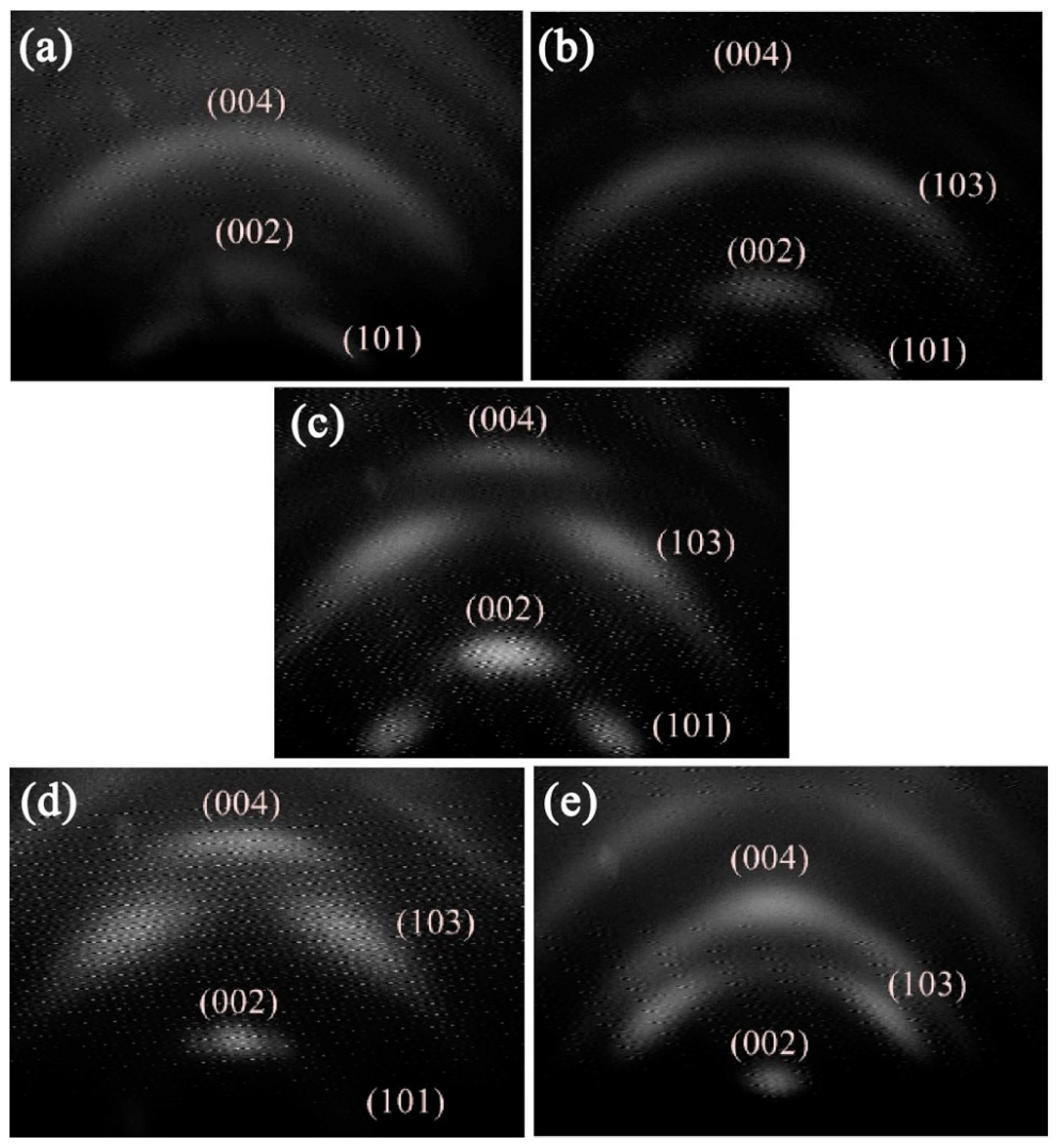
3.1. RHEED Measurement of InN Thin Films Prepared at Varying Temperatures

As shown in Figure 1, RHEED was used to characterize InN thin films prepared at different deposition temperatures. As the temperature increased from 200 to 400 °C, RHEED patterns of InN films gradually changed from continuous rings to broken rings, and the resolution of patterns became higher. However, if the temperature further increased from 400 to 600 °C, the RHEED patterns gradually changed from broken rings back to continuous rings, and the pattern resolution became lower. This indicates that the RHEED results were dramatically influenced by deposition temperature. For the temperature at 400 °C, the prepared films showed high-resolution RHEED patterns of broken rings. Further analysis reveals that only (002) and (004) diffractions appeared from the middle of the patterns. (101) and (103) crystal planes were also clearly observed at other l° cations. Prepared InN thin films showed preferential orientation at 400 °C. Their direction of growth was perpendicular to the substrate with a preferential orientation of high c-axis. Poor crystallization of prepared films was obtained at other temperatures, indicating that the optimal temperature was 400 °C.

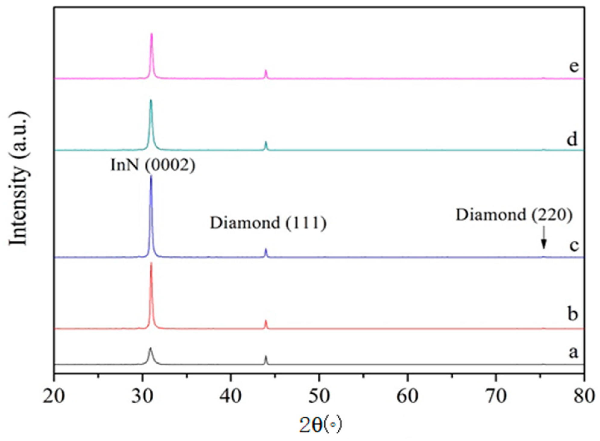
3.2. XRD of InN Thin Films Prepared at Varying Temperatures

The XRD pattern was adopted to characterize the crystallization properties of InN thin films, as shown in Figure 2. The lattice orientations at 43.9° and 75.4° are attributed to (111) and (220) diffraction peaks of the substrates. The strongest diffraction peak at 31.3° is the diffraction peak of the InN films, which is the InN (002) diffraction peak. The InN thin film sample showed a preferred orientation of high c-axis. The as-grown InN films were perpendicular to the self-standing diamond substrates. The effect of varying temperatures on the properties of the films was further studied according to Scherrer’s formula:
  d   =   0.94 λ B · cos   θ
where d is grain size, λ is wavelength of Cu Kα rays (0.15406 nm), θ is Bragg diffraction angle and B is full width at half maximum (FWHM) of the films. The stress of the films was calculated based on the stress formula:
  σ   =   2 c 13 2     c 33 ( c 11   +   c 12 ) 2 c 13 c     c 0 c 0     ( GPa )
where c11, c12, c13, c33 are elastic constants of InN crystal (c11 = 190 GPa, c33 = 182 GPa, c12 = 104 GPa, c13 = 121 GPa) [35] and c and c0 are the c-axis lattice constants of InN films and complete crystal. The variation of the stress on films prepared at different temperatures was studied. The c-axis diffraction peak positions, FWHM, grain size, tested c-axis lattice constants and calculated film stress under varying deposition temperatures are summarized in Table 1. Compared with the reported lattice constant in previous work [38], the lattice parameter is relatively large, and this is probably caused by the film stress. The increase in deposition temperature from 200 to 400 °C resulted in a gradual reduction in both c-axis lattice constant and FWHM and a gradual increase in grain size. However, a further increase in temperature from 400 to 600 °C led to a gradual growth in both c-axis lattice constant and FWHM, and a gradual decrease in grain size. Therefore, the films prepared at 400 °C have a larger grain size and smaller FWHM. Deposited by ECR-PEMOCVD system at lower temperatures, N2 (nitrogen source of the reaction) is not fully dissociated due to less efficient ionization. The dissociated particles could not move to proper positions due to lower migration energy, resulting in a poor crystallization quality of InN films. However, the films at higher temperatures exhibit higher stress, although higher temperatures improve both the ionization reaction efficiency of N2 and migration energy of particles, and the reason can be ascribed to the lattice and thermal mismatch between film and substrate [35]. According to the stress formula, the negative sign means that the value of c is larger than that of c0. This indicates that the lattice along the c-axis is lengthened and, correspondingly, the films have compression stress inside. This is probably caused by the difference in thermal expansion between InN (4 × 10⁻⁶/K) and diamond (3.7 × 10⁻⁶/K). Meanwhile, the films are InN and the substrate is diamond. They have different lattice parameters and thermal expansion. Thus, there exists a mismatch of the lattice parameter and thermal expansion during the heating process. Higher thermal stress generated interfacial defects between the films and the substrates. More importantly, a high temperature may cause the decomposition of InN films and the appearance of metal indium droplets, which would adversely deteriorate the film quality. Therefore, InN films prepared at 400 °C are of higher crystallinity, in good agreement with the RHEED results.

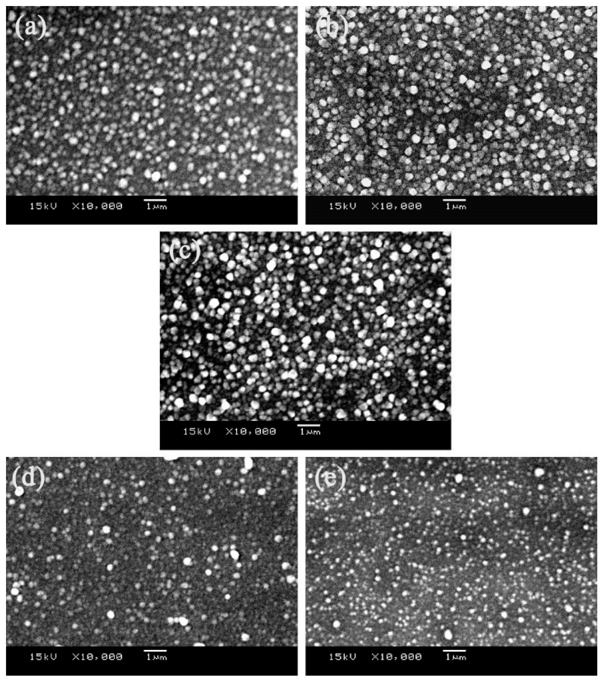
3.3. SEM Analysis of InN Thin Films Prepared at Varying Temperatures

Due to the great differences in lattice constants between InN films and self-standing diamond substrates, SEM was used to analyze InN films, as shown in Figure 3. The increase in temperature from 200 to 400 °C results in higher surface island densities of InN thin films. However, the further increase in temperature from 400 to 600 °C results in decreased surface island density of thin films, and disordered crystal grain. Figure 3 shows a typical Volmer–Weber growth mode. The corresponding process is proposed as follows. Some of the atoms which hit the substrate still have a lot of energy to return to the gas phase, while others are adsorbed on the surface of the substrate. Due to their own energy and the thermal energy gained on the substrate, atoms will drift on the substrate surface and collide with other atoms to form pairs or groups, which eventually form a condensation nucleus. When a certain concentration is reached, no new condensation nuclei are formed. The new adsorbed atoms will drift to the existing condensation nuclei, which leads to the growth of the condensation nuclei and they become small islands, and most of them form micrograins. As the islands grow, adjacent islands contact and combine with each other, so thin films with channels are formed. As the deposition continues, the adsorbed atoms fill empty channels. It is also possible to form new islands, which fill empty channels and, finally, a continuous film is formed. A proper temperature increases the migration energy of surface atoms, facilitating the formation of InN films. However, the atoms are likely to undergo secondary crystallization due to the excessively high migration energy at a relatively higher temperature.

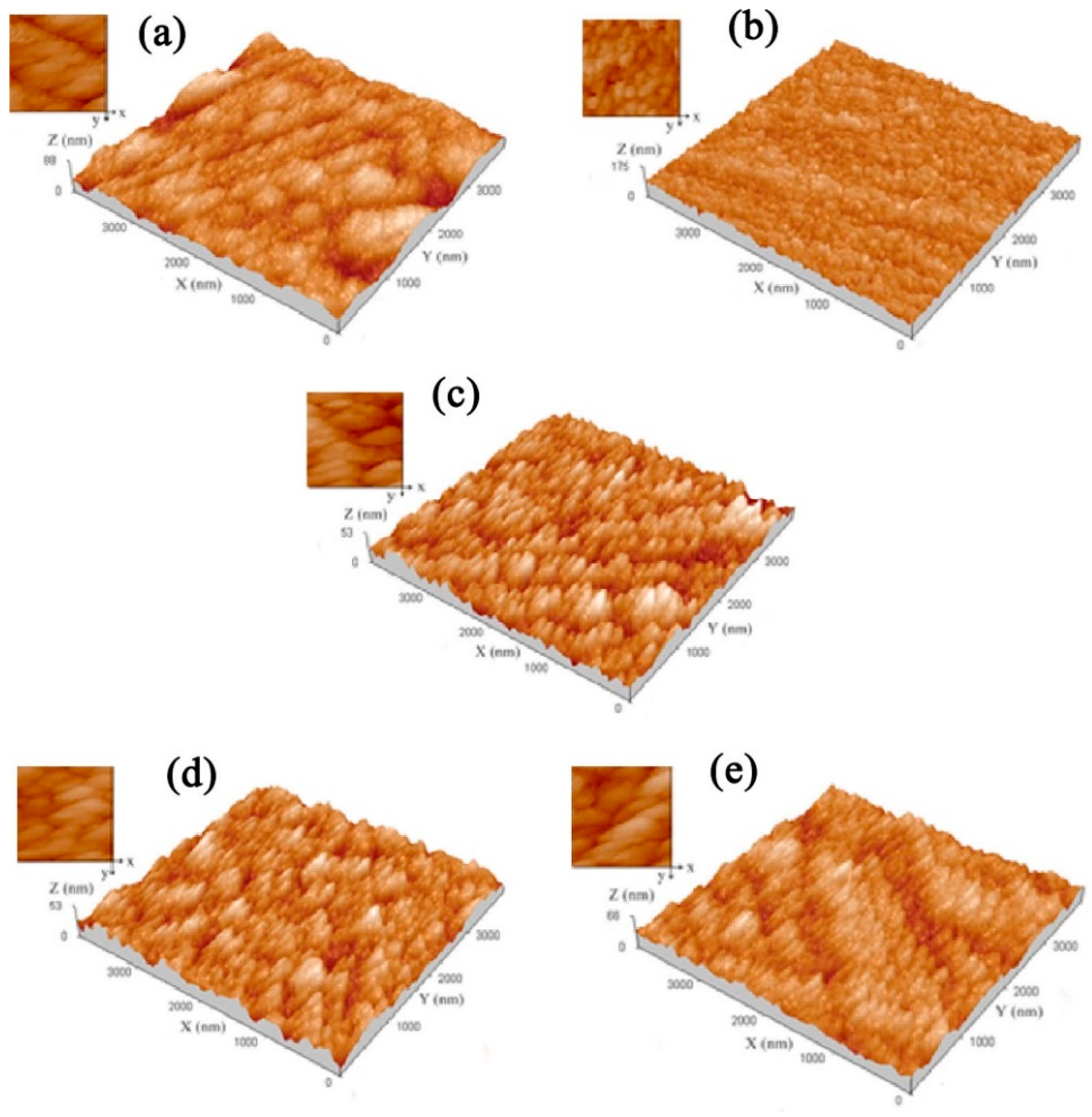
3.4. AFM Analysis of InN Thin Films Prepared at Varying Temperatures

For following up the development of photovoltaic devices based on InN, the flatness of the surface should be controlled to the nanometer level [39,40,41,42,43,44,45,46]. AFM is used to analyze surface morphology of thin films, as shown in Figure 4. The surface roughness of InN films is as low as 10 nm, fully meeting the requirements of surface flatness for a high-power infrared detector. Figure 4 shows a typical Volmer–Weber growth mode. Further analysis shows that surface island density increases as the temperature increases from 200 to 400 °C. However, a further increase in temperature from 400 to 600 °C results in reduced surface island density and disordered grains. This indicates that the temperature has a great influence on the surface morphology. At 400 °C, the prepared thin films show a smooth surface morphology formed by uniformly dense grains and visible crystal lattice boundaries. Further analysis is based on the root mean square of the surface flatness of the films. When the preparation temperature increases from 200 to 400 °C, the root mean square of the surface roughness decreases from 9.8 to 3.7 nm, and the grain size gradually becomes consistent with the same growth direction. When the temperature further increases to 600 °C, the root mean square of the surface roughness increases gradually with more disordered grain growth. Therefore, the InN film prepared at 400 °C has optimum morphological characteristics.

3.5. Electrical Properties of InN Thin Films Prepared at Varying Temperatures

The Hall effect system HL5500, manufactured by Accent, is used and the Van der Pauw method is adopted to test the electrical properties of InN thin films. Electrode contact is used and the magnetic field intensity is 0.338 T. The sample size is 1.2 cm × 1.2 cm, and four probes are located at a vertex angle of 1 cm × 1 cm in the middle of the sample surface. Because the self-standing diamond substrate is insulated, the electrical property data are all from the InN thin films. As shown in Table 2, all InN thin films exhibit the conductivity of an n-type semiconductor, which is supposed to be a unique feature of unintentionally doped InN thin films. This is related to the inherent defects in the thin films [13,14,15]. The increase in temperature from 200 to 400 °C leads to a gradual reduction in the carrier concentration but a gradual increase in the mobility of thin films. A further increase in temperature from 400 to 600 °C results in a gradual increase in the carrier concentration but a gradual decrease in the mobility of thin films. According to previous reports [14,15,16,17], higher nitrogen partial pressure leads to the generation of nitrogen vacancies, which is the main reason for the high carrier concentration during the preparation of InN thin films. InN thin films have been grown on various substrates in previous works, such as sapphire substrates [47], multicrystalline Si substrates [48] and AlN/Si substrates [49]. The mobility in InN films is mainly dominated by grain boundary scattering and defect scattering. Compared with previous reports [26,27,28], the mobility of InN films in this study is relatively low (0.68 cm2/(V·S)), but InN films could be prepared at a lower temperature by an ECR-PEMOCVD system. The inert gaseous nitrogen is used as a nitrogen source, increasing the difficulty of preparation. Subsequent work will continue to optimize the experimental parameters for the improvement of mobility. The electrical properties of prepared thin films are consistent with the XRD results. At 400 °C, InN thin films prepared on the self-standing diamond substrate show better electrical properties.

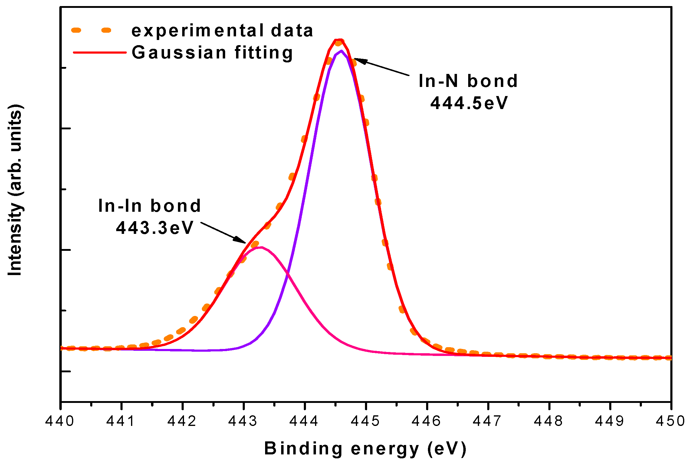
3.6. XPS Analysis of InN Thin Films Prepared at 400 °C

The above results show that the best performance of InN thin films was obtained when the deposition temperature was at 400 °C with a self-standing diamond substrate. XPS is used to study the bonding properties of our best films, as shown in Figure 5. Two peaks of 443.3 and 444.5 eV are observed, corresponding to the binding energies of In-In bonds and In–N bonds, respectively. The peak intensity of the In–N bond was significantly higher than that of the In–In bond [36,37]. This demonstrates that there are a large number of In–N bonds in our prepared films, indicating the good crystalline quality. The In–In bonds in the films correspond to indium particle formation, which originate from a large number of nitrogen vacancies generated by nitrogen atom volatilization during film preparation.

4. Conclusions

The temperature of deposition plays a key role in the preferential growth of the (0002) crystal plane of InN films. In this study, an electron cyclotron resonance plasma-enhanced metal organic chemical vapor deposition (ECR-PEMOCVD) system was used to prepare InN thin films on self-standing diamond substrates at different temperatures. The proper temperature is conducive to the optimum quality of InN films. At 400 °C, InN films with highly c-axis preferential orientations are obtained. A higher temperature results in a rougher film surface, deteriorating crystallization quality. XPS spectra show the bonding characterization of In–N and In–In in the films. The preferential orientation, optimum surface morphology and electrical properties of InN films can be obtained at a temperature of 400 °C. Given the better heat dissipation performance of self-standing diamond substrates, our achievement will be of special interest for the development of a wide range of InN-based electronic and optoelectronic devices with high power capability and sufficient power durability.

Author Contributions

Data curation, F.Q.; Formal analysis, S.W. and F.Q.; Methodology, D.Z.; Project administration, S.W.; Supervision, Y.B.; Writing–original draft, J.Z.; Writing–review & editing, J.Z.; All authors have read and agreed to the published version of the manuscript.

Funding

This work was supported by the National Natural Science Foundation of China under Grant No. 51872036, the fund of Science and Technology Project of Liaoning, China under Grant No. 2019JH8/10100057 and the innovation talent fund of Liaoning Province colleges, China under Grant No. LR2019046.

Conflicts of Interest

The authors declare no conflict of interest.

Data Availability

The data that support the findings of this study are available from the corresponding author upon reasonable request.

References

  1. Spitsyn, B.; Hsu, W.; Gorodetsky, A.; Zalavutdinov, R.; Zakharov, A.; Bouilov, L.; Stoyan, V.; Dvoryankin, V.; Chaplygin, G. AIN heteroepitaxial and oriented films grown on (111), (110) and (100) natural diamond faces. Diam. Relat. Mater. 1998, 7, 356–359. [Google Scholar] [CrossRef]
  2. Van Dreumel, G.; Buijnsters, J.; Bohnen, T.; Ter Meulen, J.; Hageman, P.; Van Enckevort, W.; Vlieg, E. Growth of GaN on nano-crystalline diamond substrates. Diam. Relat. Mater. 2009, 18, 1043–1047. [Google Scholar] [CrossRef]
  3. van Dreumel, G.W.G.; Tinnemans, P.T.; Heuvel, A.A.J.V.D.; Bohnen, T.; Buijnsters, J.G.; ter Meulen, J.J.; van Enckevort, W.J.P.; Hageman, P.R.; Vlieg, E. Realising epitaxial growth of GaN on (001) diamond. J. Appl. Phys. 2011, 110, 013503. [Google Scholar] [CrossRef] [Green Version]
  4. Dussaigne, A.; Malinverni, M.; Martin, D.; Castiglia, A.; Grandjean, N. GaN grown on (111) single crystal diamond substrate by molecular beam epitaxy. J. Cryst. Growth 2009, 311, 4539–4542. [Google Scholar] [CrossRef]
  5. Smith, M.; Cuenca, J.; Field, D.; Fu, Y. GaN-on-diamond technology platform: Bonding-free membrane manufacturing process. AIP Adv. 2020, 10, 035306. [Google Scholar] [CrossRef]
  6. Ahmed, R.; Siddique, A.; Anderson, J.; Gautam, C.; Holtz, M.; Piner, E.L. Integration of GaN and diamond using epitaxial lateral overgrowth. ACS Appl. Mater. Interfaces 2020, 12, 39397–39404. [Google Scholar] [CrossRef] [PubMed]
  7. Vo, D.D.; Vu, T.V.; Nhan, L.C.; Nguyen, C.V.; Phuc, H.V.; Tong, H.D.; Hoat, D.; Hoa, L.T.; Hieu, N.N. Theoretical prediction of electronic and optical properties of haft-hydrogenated InN monolayers. Superlattices Microstruct. 2020, 142, 106519. [Google Scholar] [CrossRef]
  8. Li, H.; Zhang, H.; Wu, H.; Hao, J.; Liu, C. Tree-like structures of InN nanoparticles on agminated anodic aluminum oxide by plasma-assisted reactive evaporation. Appl. Surf. Sci. 2019, 503, 144309. [Google Scholar] [CrossRef]
  9. Ahmad, Z.; Vernon, M.; Cross, G.B.; Deocampo, D.; Kozhanov, A. Supersaturation model for InN PA-MOCVD. arXiv 2003, arXiv:2003.10067. [Google Scholar]
  10. Pham, K.D.; Vu, T.V.; Pham, T.N.; Vo, D.D.; Dang, P.T.; Hoat, D.; Nguyen, C.V.; Phuc, H.V.; Tu, L.T.N.; Van, L.C.; et al. Tuning the electronic, photocatalytic and optical properties of hydrogenated InN monolayer by biaxial strain and electric field. Chem. Phys. 2019, 532, 110677. [Google Scholar] [CrossRef]
  11. Mekys, A.; Jurkevičius, J.; Kadys, A.; Kolenda, M.; Kovalevskij, V.; Tamulaitis, G. Influence of proton irradiation on carrier mobility in InN epitaxial layers. Thin Solid Film. 2019, 692, 137619. [Google Scholar] [CrossRef]
  12. Yamaguchi, T.; Sasaki, T.; Fujikawa, S.; Takahasi, M.; Araki, T.; Onuma, T.; Honda, T.; Nanishi, Y. In situ synchrotron X-ray diffraction reciprocal space mapping measurements in the RF-MBE growth of GaInN on GaN and InN. Crystals 2019, 9, 631. [Google Scholar] [CrossRef] [Green Version]
  13. Cui, H.; Zhang, X.; Li, Y.; Chen, D.; Zhang, Y. First-principles insight into Ni-doped InN monolayer as a noxious gases scavenger. Appl. Surf. Sci. 2019, 494, 859–866. [Google Scholar] [CrossRef]
  14. Adikimenakis, A.; Chatzopoulou, P.; Dimitrakopulos, G.P.; Kehagias, T.; Tsagaraki, K.; Androulidaki, M.; Doundoulakis, G.; Kuzmik, J.; Georgakilas, A. JSS focus issue on recent advances in wide bandgap III-nitride devices and solid state lighting: A tribute to Isamu Akasaki. ECS J. Solid State Sci. Technol. 2020, 9, 015006. [Google Scholar] [CrossRef]
  15. Weiszer, S.; Zeidler, A.; De La Mata, M.; Stutzmann, M. Growth of self-assembled and position-controlled InN nanowires on Si (111) by molecular beam epitaxy. J. Cryst. Growth 2019, 510, 56–64. [Google Scholar] [CrossRef]
  16. Dobrovolskas, D.; Arakawa, S.; Mouri, S.; Araki, T.; Nanishi, Y.; Mickevičius, J.; Tamulaitis, G. Enhancement of InN luminescence by introduction of graphene interlayer. Nanomaterials 2019, 9, 417. [Google Scholar] [CrossRef] [Green Version]
  17. An, Y.; He, Y.; Wei, H.; Liu, S.; Li, M.; Song, Y.; Qiu, P.; Rehman, A.; Zheng, X.; Peng, M. Metallic indium segregation control of InN thin films grown on Si(100) by plasma-enhanced atomic layer deposition. Results Phys. 2019, 12, 804–809. [Google Scholar] [CrossRef]
  18. Barick, B.K.; Rodríguez-Fernández, C.; Cantarero, A.; Dhar, S. Structural and electronic properties of InN nanowire network grown by vapor-liquid-solid method. AIP Adv. 2015, 5, 057162. [Google Scholar] [CrossRef] [Green Version]
  19. Kucera, M.; Adikimenakis, A.; Dobročka, E.; Kúdela, R.; Ťapajna, M.; Laurenčíková, A.; Georgakilas, A.; Kuzmík, J. Structural, electrical, and optical properties of annealed InN films grown on sapphire and silicon substrates. Thin Solid Film. 2019, 672, 114–119. [Google Scholar] [CrossRef]
  20. Miyoshi, M.; Yamanaka, M.; Egawa, T.; Takeuchi, T. Microstructure variation in thick AlInN films grown on c-plane GaN on sapphire by metalorganic chemical vapor deposition. J. Cryst. Growth 2019, 506, 40–44. [Google Scholar] [CrossRef]
  21. Fang, X.; Zheng, F.; Drachenko, O.; Zhou, S.; Zheng, X.; Chen, Z.; Wang, P.; Ge, W.; Shen, B.; Feng, J.; et al. Determination of electron effective mass in InN by cyclotron resonance spectroscopy. Superlattices Microstruct. 2019, 136, 106318. [Google Scholar] [CrossRef]
  22. Liu, J.; Liu, H.; Zhang, A.; Wang, J.; Tang, G.; Zhang, J.; Bai, D. Strain dependent electronic structure and optical properties tuning of InN/PtX2 (X = S, Se) van der waals heterostructures. Vacuum 2019, 168, 108805. [Google Scholar] [CrossRef]
  23. Akasaka, T.; Schied, M.; Kumakura, K. N-face GaN/InN/GaN double heterostructures emitting near-infrared photoluminescence grown by metalorganic vapor phase epitaxy. Appl. Phys. Express 2018, 11, 081001. [Google Scholar] [CrossRef]
  24. Xie, Z.; Zhang, R.; Liu, B.; Li, L.; Liu, C.; Xiu, X.; Zhao, H.; Han, P.; Gu, S.; Shi, Y.; et al. The high mobility InN film grown by MOCVD with GaN buffer layer. J. Cryst. Growth 2007, 298, 409–412. [Google Scholar] [CrossRef]
  25. Zhu, X.; Guo, L.W.; Peng, M.; Ge, B.; Zhang, J.; Ding, G.; Jia, H.; Chen, H.; Zhou, J. Characterization of a-plane InN film grown on r-plane sapphire by MOCVD. J. Cryst. Growth 2008, 310, 3726–3729. [Google Scholar] [CrossRef]
  26. Darakchieva, V.; Lorenz, K.; Barradas, N.P.; Alves, E.; Monemar, B.; Schubert, M.; Franco, N.; Hsiao, C.-L.; Chen, L.-C.; Schaff, W.J.; et al. Hydrogen in InN: A ubiquitous phenomenon in molecular beam epitaxy grown material. Appl. Phys. Lett. 2001, 79, 1489. [Google Scholar] [CrossRef] [Green Version]
  27. De, A.; Tangi, M.; Shivaprasad, S.M. Pre-nitridation induced In incorporation in InxGa1−xN nanorods on Si(111) grown by molecular beam epitaxy. J. Appl. Phys. 2015, 118, 025301. [Google Scholar] [CrossRef]
  28. Yamamoto, A.; Tanaka, T.; Koide, K.; Hashimoto, A. Improved electrical properties for metalorganic vapour phase epitaxial InN films. Phys. Status Solidi 2002, 194, 510–514. [Google Scholar] [CrossRef]
  29. Krischok, S.; Yanev, V.; Balykov, O.; Himmerlich, M.; Schaefer, J.; Kosiba, R.; Ecke, G.; Cimalla, I.; Cimalla, V.; Ambacher, O.; et al. Investigations of MBE grown InN and the influence of sputtering on the surface composition. Surf. Sci. 2004, 849, 566–568. [Google Scholar] [CrossRef]
  30. Wen-Cheng, K.; Chih-Yung, C.; Widi, S. InGaN-based light-emitting diodes grown on various aspect ratios of concave nanopattern sapphire substrate. Appl. Surf. Sci. 2018, 456, 967–972. [Google Scholar]
  31. Roul, B.; Rajpalke, M.K.; Bhat, T.N.; Kumar, M.; Kalghatgi, A.T.; Krupanidhi, S.B. GaAs metal-oxide-semiconductor based nonvolatile memory devices embedded with ZnO quantum dots. J. Cryst. Growth 2012, 354, 208. [Google Scholar] [CrossRef]
  32. Tallaire, A.; Mille, V.; Brinza, O.; Thi, T.N.T.; Brom, J.M.; Loguinov, Y.; Katrusha, A.; Koliadind, A.; Achard, J. Birefringence microscopy of unit dislocations in diamond. Diam. Relat. Mater. 2017, 77, 146. [Google Scholar] [CrossRef]
  33. Gicquel, A.; Hassouni, K.; Silva, F.; Achard, J. Polycrystalline diamond characterisations for high end technologies. Curr. Appl. Phys. 2020, 1, 479. [Google Scholar] [CrossRef]
  34. Schwander, M.; Partes, K. A review of diamond synthesis by CVD processes. Diam. Relat. Mater. 2011, 20, 1287–1301. [Google Scholar] [CrossRef]
  35. Lobaev, M.A.; Gorbachev, A.; Bogdanov, S.; Vikharev, A.; Radishev, D.; Isaev, V.; Chernov, V.; Drozdov, M. Influence of CVD diamond growth conditions on nitrogen incorporation. Diam. Relat. Mater. 2017, 72, 1–6. [Google Scholar] [CrossRef]
  36. Zhi, A.-B.; Qin, F.; Zhang, N.; Bian, J.; Yu, B.; Zhou, Z.-F.; Jiang, X. Low-temperature growth of highly c-oriented InN films on glass substrates with ECR-PEMOCVD. Vacuum 2012, 86, 1102–1106. [Google Scholar] [CrossRef]
  37. Bi, Z.; Ek, M.; Stankevič, T.; Colvin, J.; Hjort, M.; Lindgren, D.; Lenrick, F.; Johansson, J.; Wallenberg, R.; Timm, R.; et al. Self-assembled InN quantum dots on side facets of GaN nanowires. J. Appl. Phys. 2018, 16, 164302. [Google Scholar] [CrossRef]
  38. Zhang, N.; Qin, F.; Bai, Y.; Bian, J.; Li, S.; Pan, L.; Zhi, A.; Liu, X.; Jiang, X. Effect of buffer layer on the structural and morphological properties of GaN films grown with ECR-PEMOCVD. Diam. Relat. Mater. 2012, 21, 88–91. [Google Scholar] [CrossRef]
  39. Sun, J.; Bai, Y.; Yang, T.; Xu, Y.; Wang, X.; Du, G.; Wu, H. Deposition of ZnO films on freestanding CVD thick diamond films. Chin. Phys. Lett. 2006, 23, 1321. [Google Scholar]
  40. Sun, J.; Bai, Y.-Z.; Yang, T.-P.; Sun, J.-C.; Du, G.-T.; Jiang, X.; Wu, H.-H. Preparation and characteristics of ZnO films on freestanding diamond substrates. Diam. Relat. Mater. 2007, 16, 1597–1601. [Google Scholar] [CrossRef]
  41. Wang, K.; Reeber, R.R. Primary pyroelectric transition temperatures of binary nitrides. Appl. Phys. Lett. 2001, 79, 11. [Google Scholar]
  42. Lee, I.; Yu, C.; Shin, H.; Kim, J.; Lee, Y.; Hur, T.; Kim, H. Growth and nanostructure of InN thin films deposited by reactive magnetron sputtering. Thin Solid Films 2007, 515, 4691. [Google Scholar] [CrossRef]
  43. Takai, O.; Ikuta, K.; Inoue, Y. Some properties of group-III nitride thin films directly grown on non-single-crystalline substrates by using a molecular beam epitaxy apparatus. Thin Solid Films 1998, 318, 148. [Google Scholar] [CrossRef]
  44. Serrano, J.; Rubio, A.; Hernandez, E.; Munoz, A.; Mujica, A. First-principles investigations on metallic silicon allotropes. Phys. Rev. B. 2000, 62, 16612. [Google Scholar] [CrossRef] [Green Version]
  45. Qian, Z.; Shen, W.; Ogawa, H.; Guo, Q. Capacitance characteristics in InN thin films grown by reactive sputtering on GaAs. Prog. Phys. 2003, 23, 257–283. [Google Scholar]
  46. Novikov, M.V.; Maystrenko, A.L.; Kushch, V.I. Effect of metal catalyst thermal expansion on thermal stability of synthetic diamonds. Comput. Mater. Sci. 2012, 53, 409–415. [Google Scholar] [CrossRef]
  47. Cross, G.B.; Ahmad, Z.; Seidlitz, D.; Vernon, M.; Dietz, N.; Deocampo, D.; Gebregiorgis, D.; Lei, S.; Kozhanov, A. Kinetically stabilized high-temperature InN growth. J. Cryst. Growth 2020, 536, 125574. [Google Scholar] [CrossRef]
  48. Sato, Y.; Saito, S.; Shiraishi, K.; Taniguchi, S.; Izuka, Y.; Saito, T. Vertical alignment of InN- and GaN-based nanopillar crystals grown on a multicrystalline Si substrate. J. Cryst. Growth 2020, 537, 125603. [Google Scholar] [CrossRef]
  49. Chen, W.-C.; Chen, H.-P.; Lin, Y.-W.; Liu, D.-R. Growth of narrow substrate temperature window on the crystalline quality of InN epilayers on AlN/Si(111) substrates using RF-MOMBE. J. Cryst. Growth 2019, 522, 204–209. [Google Scholar] [CrossRef]
Figure 1. Reflection high-energy electron diffraction (RHEED) patterns of the InN thin films deposited at (a) 200 °C, (b) 300 °C, (c) 400 °C, (d) 500 °C and (e) 600 °C.
Coatings 10 01185 g001
Figure 2. XRD patterns of InN thin films deposited at (a) 200 °C, (b) 300 °C, (c) 400 °C, (d) 500 °C and (e) 600 °C.
Coatings 10 01185 g002
Figure 3. SEM patterns of the InN thin films deposited at (a) 200 °C, (b) 300 °C, (c) 400 °C, (d) 500 °C and (e) 600 °C.
Coatings 10 01185 g003
Figure 4. AFM patterns of the InN thin films deposited at (a) 200 °C, (b) 300 °C, (c) 400 °C, (d) 500 °C and (e) 600 °C.
Coatings 10 01185 g004
Figure 5. In 3d5/2 XPS spectra of the InN thin films deposited at 400 °C.
Coatings 10 01185 g005
Table 1. InN (0002) diffraction peak position, full width at half maximum (FWHM), grain size, lattice constant and stress.
SampleTemperature (°C)2θ (°)FWHM (°)Size (nm)Lattice Constant c0 (nm)Stress σ (GPa)
a20031.170.38260.5746−0.69
b30031.270.24310.5724−1.24
c40031.300.17470.5708−1.96
d50031.260.28310.5737−2.52
e60031.190.31280.5758−3.42
Table 2. Electrical properties of InN films on diamond substrates deposited at various temperatures.
SampleTemperature (°C)Mobility (cm2/(V·S))Carrier Concentration (1020 cm−3)Conductivity (Scm−1)
a20021.72.05711.8
b30032.51.24644.8
c40048.50.92713.9
d50038.41.15706.6
e60024.21.78689.2
Publisher’s Note: MDPI stays neutral with regard to jurisdictional claims in published maps and institutional affiliations.

