Article

Energy-Efficient Training of Memristor Crossbar-Based Multi-Layer Neural Networks

1
Center for Computational and Data Sciences, Independent University, Bangladesh, Dhaka 1229, Bangladesh
2
Department of Electrical and Computer Engineering, University of Dayton, Dayton, OH 45469, USA
*
Author to whom correspondence should be addressed.
Chips 2025, 4(3), 38; https://doi.org/10.3390/chips4030038
Submission received: 30 July 2025 / Revised: 26 August 2025 / Accepted: 2 September 2025 / Published: 5 September 2025
(This article belongs to the Special Issue IC Design Techniques for Power/Energy-Constrained Applications)

Abstract

Memristor crossbar-based neural network systems offer high throughput with low energy consumption. A key advantage of on-chip training in these systems is their ability to mitigate the effects of device variability and faults. This paper presents an efficient on-chip training circuit for memristor crossbar-based multi-layer neural networks. We propose a novel method for storing the product of two analog signals directly in a memristor device, eliminating the need for ADC and DAC converters. Experimental results show that the proposed system is approximately twice as energy efficient and 1.5 times faster than existing memristor-based systems for training multi-layer neural networks.

1. Introduction

With the emergence of IoT technology, computation is increasingly shifting toward edge devices [1]. Many applications require the execution of Artificial Intelligence (AI) algorithms on edge devices in real time. These devices are often constrained by size, weight, and power (SWaP). Neural networks are widely used in pattern recognition and signal processing applications. Specialized architectures for neural networks can provide high-throughput, low-power execution at the edge [2,3].
Frequent access to synaptic weight values from memory to processing units is a major source of performance and energy inefficiency in neural network execution [4]. Processing-in-memory computing systems offer a promising solution to this challenge. However, as device sizes continue to shrink, process variations and fault tolerance have become increasingly critical concerns in computing system design.
Memristor devices [5,6] have received significant interest as a synaptic element in a neuromorphic system [7,8]. Memristor devices, in a crossbar structure, perform multiple multiply–add operations in parallel in the analog domain. This inherent parallelism leads to the development of highly dense, computationally efficient neuromorphic systems [2].
To ensure the proper functionality of a memristor crossbar-based neural network (MCNN), an efficient training system is essential. Training can be performed either off-chip or on-chip. Off-chip training offers the advantage of implementing any training algorithm in software while leveraging the computational power of high-performance computer clusters. However, accurately modeling memristor crossbars in software remains challenging due to issues such as sneak paths and device variations [9,10].
On-chip training requires the hardware implementation of the training algorithm directly on the chip. Training data are applied to the system, and the conductivity of memristors—representing synaptic weights—is updated iteratively [7]. This method provides greater tolerance to device variations and faults. In this work, we present an efficient on-chip training circuit for multi-layer MCNNs based on the back-propagation (BP) learning algorithm.
IBM recently designed and fabricated a 64-core processing-in-memory chip based on phase-change memory devices for deep neural network inference. This system employs ex situ training and relies on analog-to-digital converter (ADC) circuits during inference [11]. Several prior studies have explored on-chip training of MCNNs [12,13,14]. Soudry et al. [12] proposed an in situ training system in which each synapse was implemented using two transistors and one memristor. In contrast, the proposed work implements each synapse using only two memristors in the neuron circuit.
During training, the synaptic weights of neurons are updated iteratively based on the corresponding input and delta/error term. The delta/error term of a neuron is computed as the product of two components: the back-propagated error and the derivative of the activation function. The work in [13] designed an on-chip training system for MCNNs using ADC and DAC circuits. Additionally, a digital multiplier was employed to evaluate the delta/error term of each neuron.
In this work, we propose a novel technique for storing the product of two analog signals directly in a memristor device. This technique is used to store the error term of a neuron as required by the training algorithm. We designed a complete training circuit and demonstrated successful training on several nonlinearly separable datasets. Unlike previous approaches, such as [13], the proposed technique eliminates the need for costly ADC and DAC converters. As a result, it enables faster training of MCNNs while significantly reducing energy consumption.
The rest of the article is organized as follows: Section 2 describes related work in the area. Section 3 describes a memristor-based neuron circuit and a memristor-based analog storage circuit. Section 4 describes the hardware implementation of the proposed training technique. Section 5 and Section 6 describe the experimental setup and results, respectively. Finally, Section 7 concludes the article.

2. Related Works

Boquet et al. proposed an ex situ training technique for MCNNs to mitigate the impact of device-to-device variation [15]. During training, they added some variation to the weights to make the network tolerant against that variation. Alibart et al. demonstrated ex situ and in situ training of memristor crossbar-based linear classifiers using the perceptron learning rule [16]. They have not examined the training of nonlinearly separable problems and have not provided details of the ex situ and in situ training circuits. IBM designed and fabricated a 64-core processing in-memory chip based on a phase-change memory device for the inference operation of deep neural networks [11]. They utilized ex situ training and the ADC circuit in the system.
Zhang et al. [17] designed a hybrid spiking neuron circuit combining memristor and CMOS devices. They demonstrated a fully hardware execution of a spiking neural network based on the hybrid neuron circuit. Singh et al. developed a hardware–software co-design framework for implementing memristor-based deep neural networks [18], which considered various non-idealities such as memristor device variations. The memristor crossbar circuit in the simulator utilized ADC, DAC converters, and peripheral circuitry for writing.
Shen et al. simulated a realistic memristor device by adding random noise to the Vteam memristor model [19]. They introduced a dynamic threshold technique to enhance the in situ training accuracy of an MCNN. However, they have not examined the design of the gradient calculation circuit. Zhang et al. developed a fully integrated memristor chip having on-chip learning capability [20]. They utilized a 1T1R crossbar array and ADC circuit in the design. Gao et al. developed a brain-like algorithm and architecture utilizing a 1T1R crossbar array [21]. They demonstrate in situ learning ability for the sound localization task on the system.
Work in [22] demonstrated in situ training of multi-layer MCNNs. For each layer of neurons, they proposed to use two instances of the synaptic weights in the hardware: one set for the forward pass and a transposed version for the backward pass. However, due to the stochastic behavior of memristor devices, it is practically difficult to create an exact copy of a memristor crossbar.
Soudry et al. [12] proposed an in situ method for memristor-based neural networks based on the gradient descent learning rule. They used two transistors and one memristor to implement a synaptic weight. Work in [13] designed an on-chip training system for multi-layer MCNNs based on the back-propagation learning algorithm. They used ADC and DAC circuits during training. In addition to that, a digital multiplier was used to evaluate the delta/error term of the neurons.
Work in [14] proposed a variant of the back-propagation learning algorithm for an efficient hardware implementation. In the training rule, they only considered the sign of the neuron error term. Fernando et al. explored the implementation of multi-layer MCNNs using 3D-stacked memristor crossbar arrays [23]. They used different layers of the 3D memristor array to implement different layers of a neural network and adopted a training technique similar to that used in [13].

3. Memristor-Based Neuron and Storage Circuit

A memristor is a nonvolatile device exhibiting a variable resistance state [5]. Several research groups have fabricated memristor devices using various materials. These devices are classified into electrical, optoelectronic, and ionic types based on their switching mechanisms. Electrical memristors operate through electron transport and conductive filament formation [9,24], making them suitable for artificial neural network implementation. Optoelectronic memristors respond to both electrical and optical stimuli [25], enabling applications in machine vision and photonic computing. Ionic memristors rely on ion migration within the device [26], providing analog switching behavior that closely mimics biological synapses for neuromorphic computing. In this work, an electrical memristor device is employed to implement a multi-layer artificial neural network.
Shimeng et al. fabricated an electrical memristor device using TiN/HfOx/AlOx/Pt thin-film stacks [9]. The thicknesses of the layers in this device are 50 nm, 5 nm, 5 nm, and 50 nm, respectively [27]. Table 1 presents the parameters for this device. Memristor devices arranged in a highly dense two-dimensional grid are referred to as a crossbar array [16].

3.1. Neuron Circuit

This work utilizes the memristor-based neuron circuit shown in Figure 1. The circuit has four inputs, with each synapse implemented using a pair of memristors. Each input is connected to two virtually grounded operational amplifiers (op-amps) through its corresponding pair of memristors. For a given input (x1), the synaptic weight is represented by the difference in conductance between the memristors connected to the first (Column+) and second (Column−) columns (σx1+ − σx1−).
In Figure 1, the bottoms of the memristor crossbar columns are connected to virtually grounded op-amps. As a result, the currents through the first and second column wires are, respectively, x 1 . σ x 1 + + + x 4 . σ x 4 +   and x 1 . σ x 1 + + x 4 . σ x 4 . The second op-amp (directly connected to Column−) generates the neuron output yj. In the non-saturating region of this op-amp, the output yj of the neuron circuit is expressed as
y j = R f x 1 . σ x 1 + + + x 4 . σ x 4 + { x 1 . σ x 1 + + x 4 . σ x 4 } = R f x 1 . σ x 1 + σ x 1 + + x 4 . σ x 4 + σ x 4
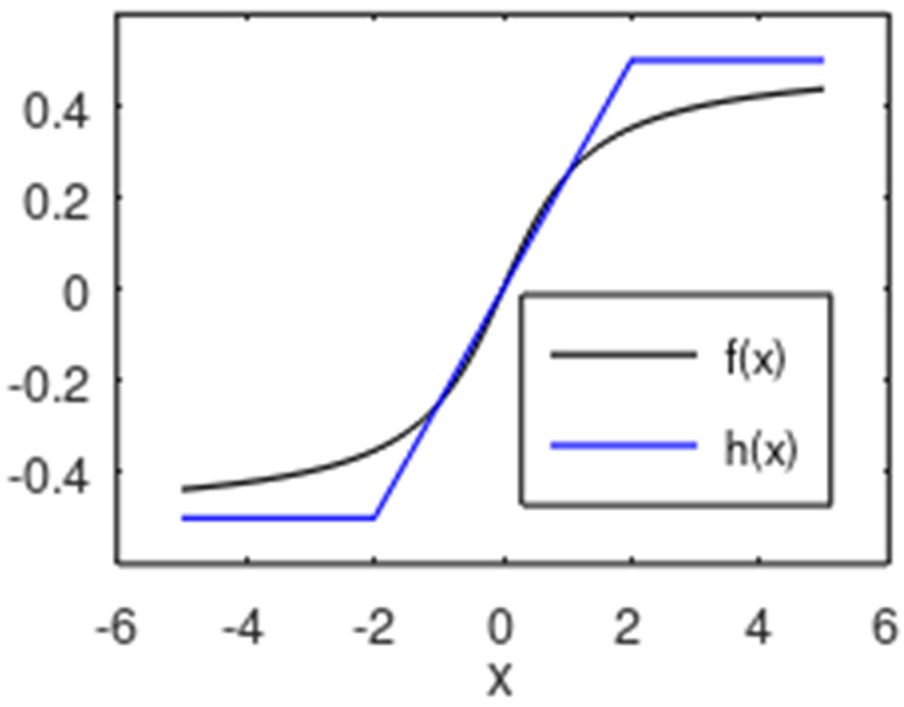
We assume that D P j = 4 R f x 1 . σ x 1 + σ x 1 + + x 4 . σ x 4 + σ x 4 . Then, in the non-saturating region of this op-amp, yj = DPj/4. We set the power rails of the op-amps VDD and VSS to 0.5 V and −0.5 V, respectively. As a result, the neuron circuit implements the activation function h(x) as shown in Equation (1). This implies that the neuron circuit evaluates the function h(DPj).
h ( x ) = 0.5           i f   x > 2 x 4               i f   x < 2 0.5         i f   x < 2
The Figure 2 graph shows that the function h(x) closely approximates the activation function, f x = 1 π t a n 1 ( x ) . The values of VDD and VSS are chosen to ensure that no memristor has more than Vth across it during inference [28].

3.2. Memristor-Based Analog Storage Circuit

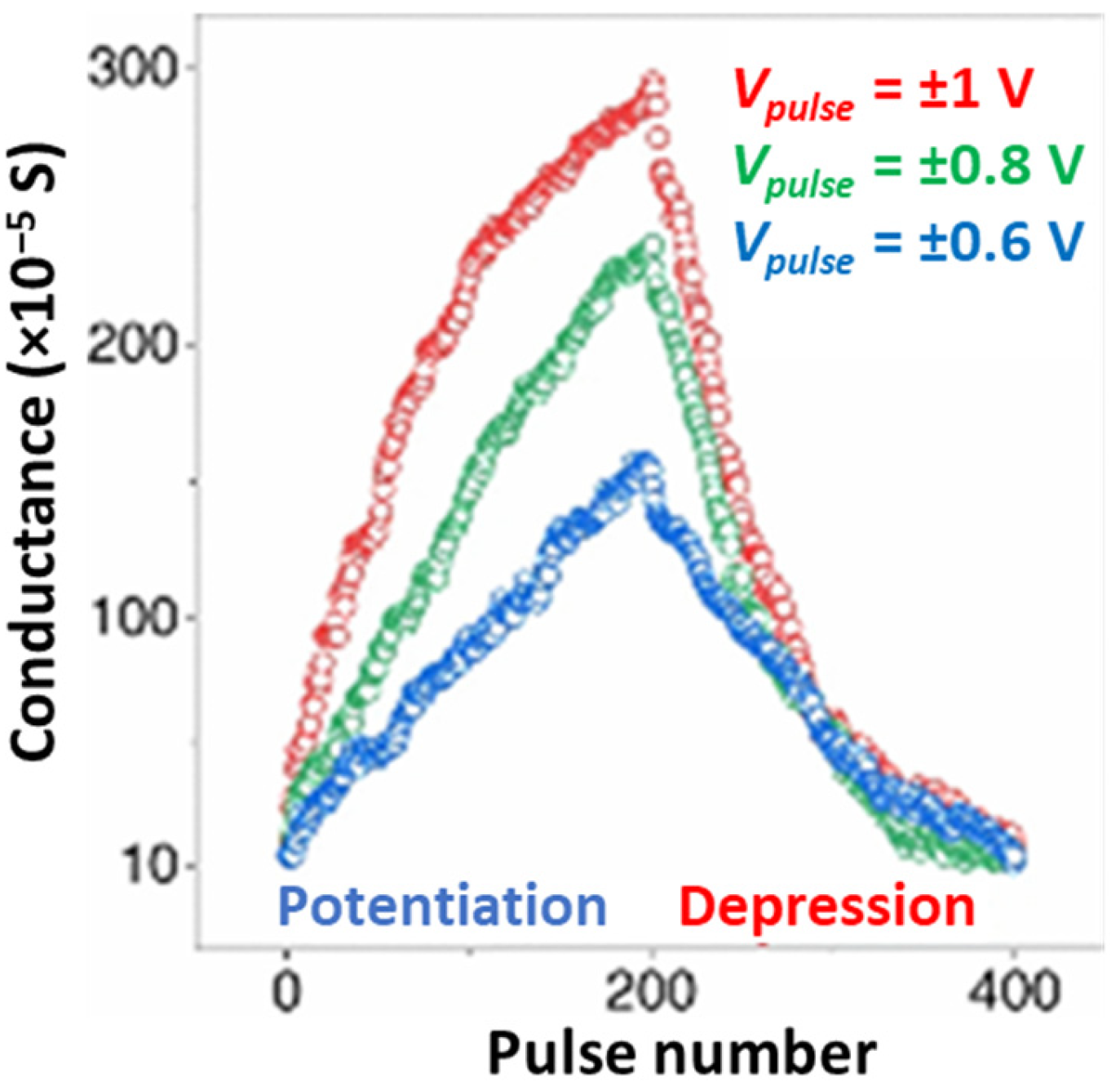
Figure 3 presents the characterization data of a memristor device reported in [29]. The figure shows that the device conductance increases almost linearly with the duration of the applied voltage, up to a certain conductance limit.
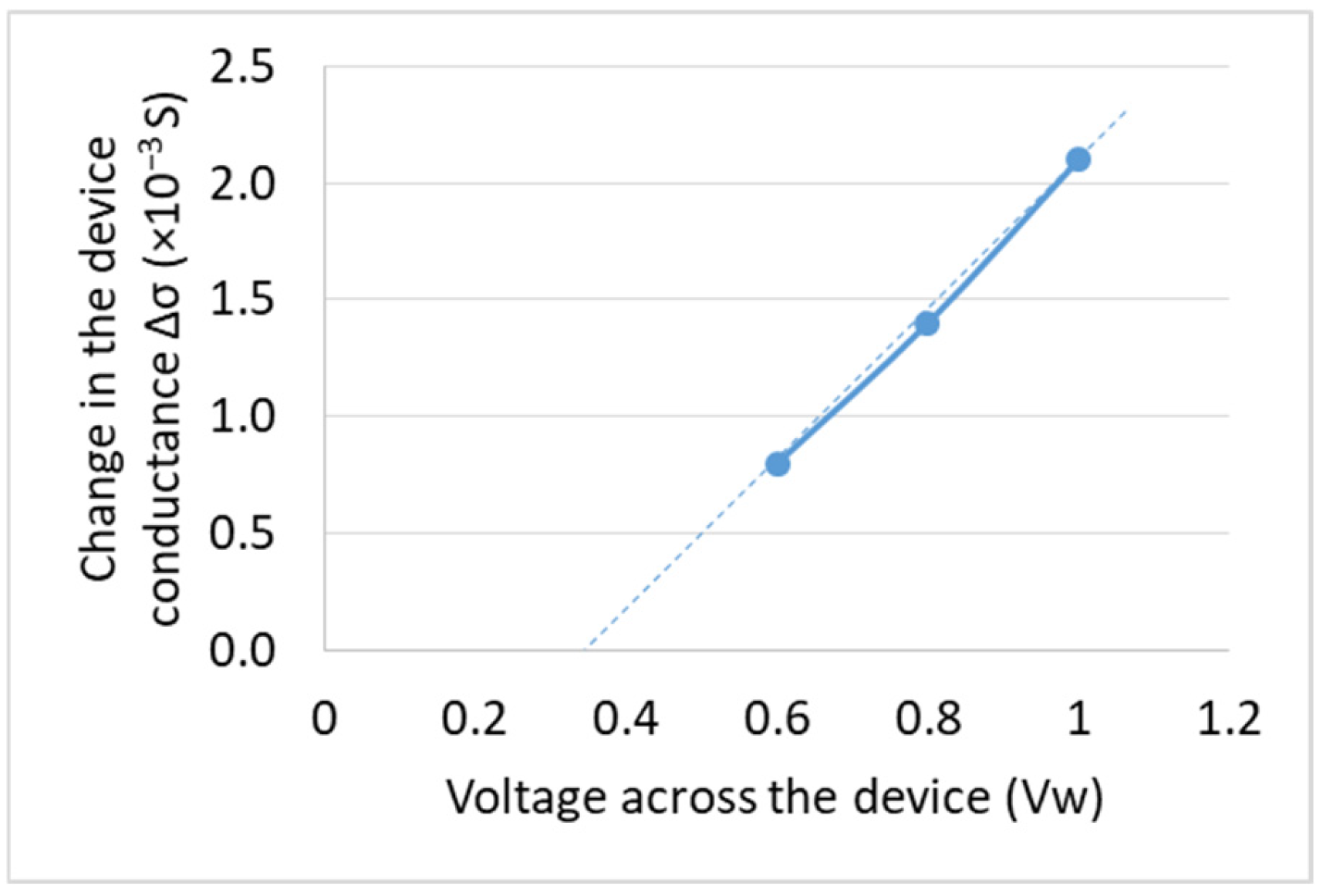
Figure 4 shows the change in device conductance with respect to different write voltage amplitudes of the same duration (extracted from Figure 3). The results indicate that the change in conductance is approximately linearly proportional to (VwVt), where Vw is the write voltage and Vt is the device threshold voltage (a constant) [28].
An analog signal can be stored in a memristor device as a change in its conductance value. In this article, we propose storing the product of two analog signals in a memristor. The device conductance is first initialized to the σoff state (the lowest conductance level). For storage, the amplitude of the voltage pulse applied across the device is determined by one signal, while the pulse duration is determined by the other. This approach is valid because if x ∝ a and x ∝ b, then x ∝ ab.
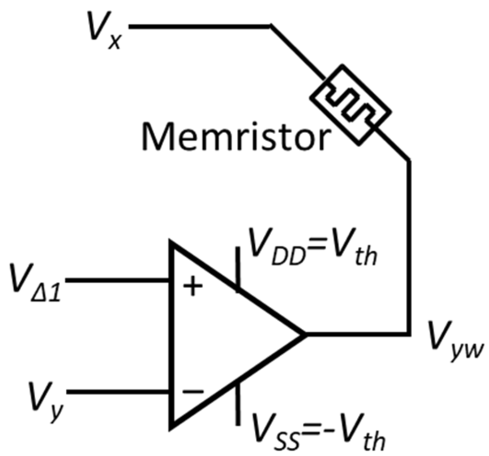
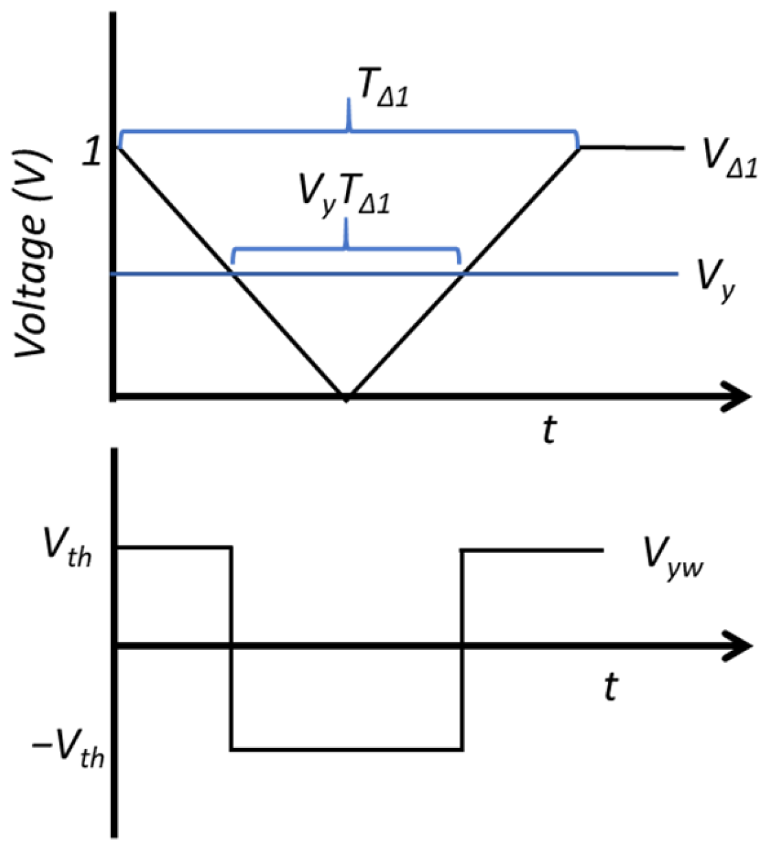
The circuit to store the product of two analog voltages in a memristor device is shown in Figure 5. The waveform VΔ1 used in this circuit is shown in Figure 6. The magnitude of Vyw is −Vth for the duration VyTΔ1, where TΔ1 is a constant. For the remaining time, the magnitude is Vth. For duration VyTΔ1, the potential difference across the memristor in Figure 5 is Vx + Vth. This induces a change in the conductance proportional to VxVy.
V Δ 1 ( t ) = 1 2 t T Δ 1                   i f   0 t T Δ 1 / 2 2 t T Δ 1 1                     i f T Δ 1 2 < t T Δ 1 1                     o t h e r w i s e
We validated the effectiveness of using a memristor device to store the product of two analog voltages through simulation. The initial conductance of a memristor device was set to 1 × 10⁻⁷ S. We estimate the ratio of the changes in conductance for (2.5 V, 70 ns) and (1.5 V, 35 ns) pulses, which is ((2.5 − 1.4)/(1.5 − 1.4)) × (70/35) or 22. Table 2 shows the change in conductance obtained from simulation using an accurate memristor device model [30] for (2.5 V, 70 ns) and (1.5 V, 35 ns) pulses. The ratio of the conductance values obtained from the simulation is 21, which is close to the estimated ratio.

4. Training of Memristor Crossbar-Based Multi-Layer Neural Networks

4.1. Multi-Layer Neural Network Design

The design of a nonlinear separator requires a multi-layer neural network with a nonlinear activation function for the neurons. Figure 7 illustrates the implementation of a two-layer network consisting of four inputs, three neurons in the first layer, and four neurons in the output layer, using the memristor crossbar-based neuron circuit shown in Figure 1. The circuit employs two memristor crossbars, each implementing the synapses of one neural layer.

4.2. Training Algorithm

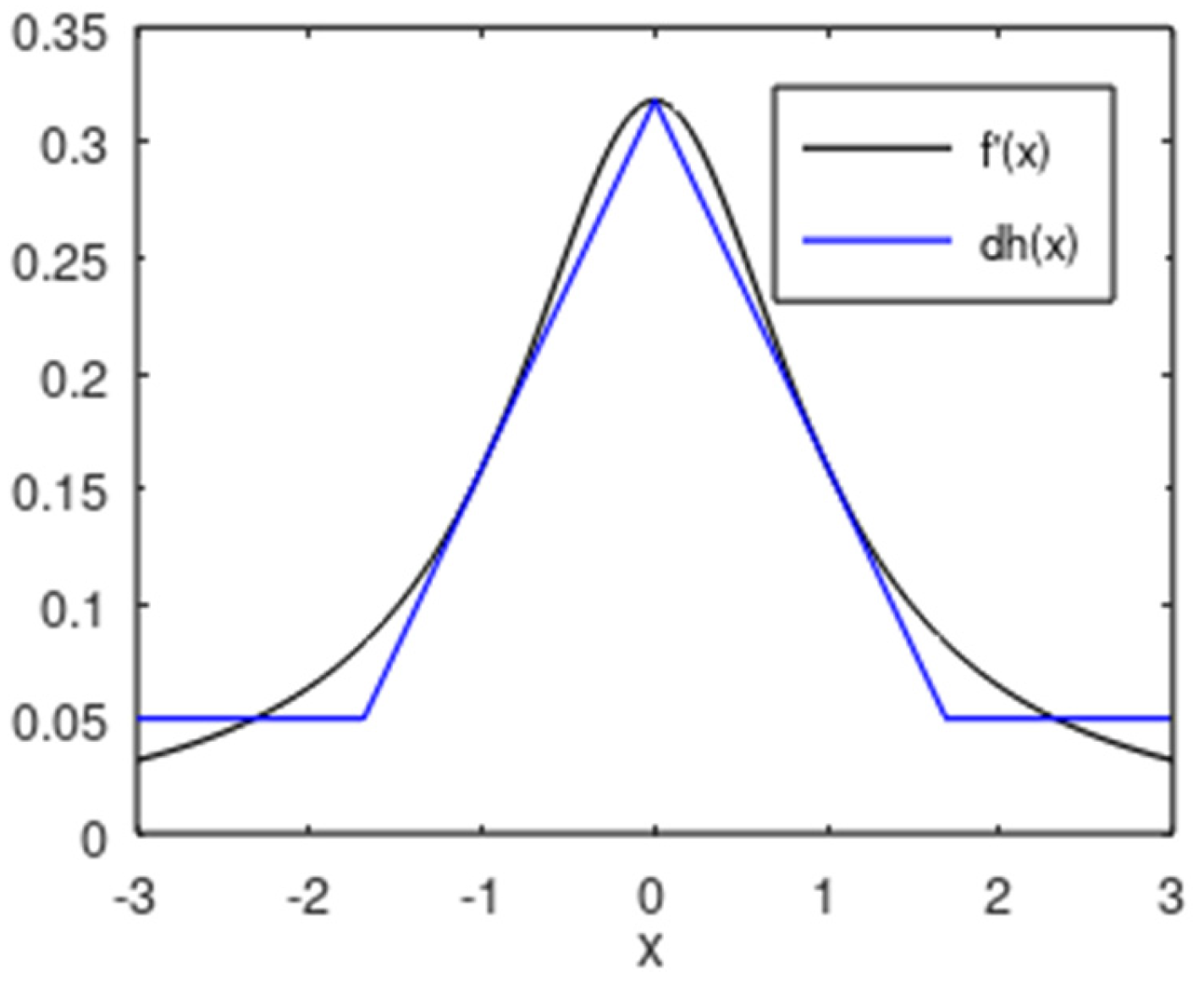
The hardware implementation of the exact back-propagation (BP) learning algorithm is costly, as it requires components such as ADCs, DACs, lookup tables for evaluating the derivative of the activation function, and multipliers [13]. To address this issue, we propose a variant of the stochastic BP algorithm designed for low-cost hardware implementation, which eliminates the need for expensive ADC and DAC components. To further simplify the weight update operation, the derivative of the activation function f’(x) is approximated by the function dh(x), as defined in Equation (3). Figure 8 demonstrates that dh(x) closely approximates f’(x).
d h ( x ) = ( 1 | x | / 2 ) / π ,   x < 1.67 0.05 ,   e l s e
The proposed training algorithm for efficient hardware implementation is mentioned below:
(1)
Apply random number of pulses across the memristor devices in the synaptic arrays.
(2)
For each training data (x, t), execute the following steps:
(i)
Apply the input x to the layer 1 crossbar and evaluate the DPj and, yj values of all the neurons in the system (layer 1 and output layer neurons).
(ii)
Calculate the error δj for each output layer neuron j based on Equation (4).
δ j = ( t j y j ) f ( D P j )         ( t j y j ) d h ( D P j )
(iii)
Assume that the hidden layer neuron j is connected to the output layer neuron k and w k , j is the corresponding synaptic weight. Back-propagate the output layer errors for each hidden layer neuron j based on the following formula.
δ j = ( k δ k w k , j × f ( D P j ) ) ( k δ k w k , j × d h ( D P j ) )
(iv)
Determine the amount, Δw, that each neuron’s synapses should be updated.
Δ w j = 2 η × δ j × x
where 2η is the learning rate.
(3)
Repeat Step 2 until the output layer error is converged to a sufficiently small value.

4.3. Hardware Implementation of the Proposed Training Algorithm

This subsection describes the hardware implementation of the proposed training algorithm for the neural network shown in Figure 7. A similar approach can be applied to three-layer or deeper neural networks. The implementation of the training algorithm is divided into the following four steps:
(i)
Forward pass: Apply input and evaluate the network output.
(ii)
Calculate the output layer neuron errors.
(iii)
Back-propagate the error for layer 1 neurons.
(iv)
Update the synaptic weights.
The hardware implementation of these steps is detailed below:
Step 1: In the MCNN shown in Figure 7, a set of inputs is applied to the layer 1 crossbar, and the outputs of both layer 1 and layer 2 neurons are evaluated. In Equations (4) and (5), the function dh(x) must be computed for the dot product of the neuron inputs and weights (DPj). The DPj value for neuron j corresponds to the difference in currents through the Column+ and Column− wires in the neuron circuit (Figure 1). It can be approximated from the corresponding neuron output yj as DPj = 4 × yj.
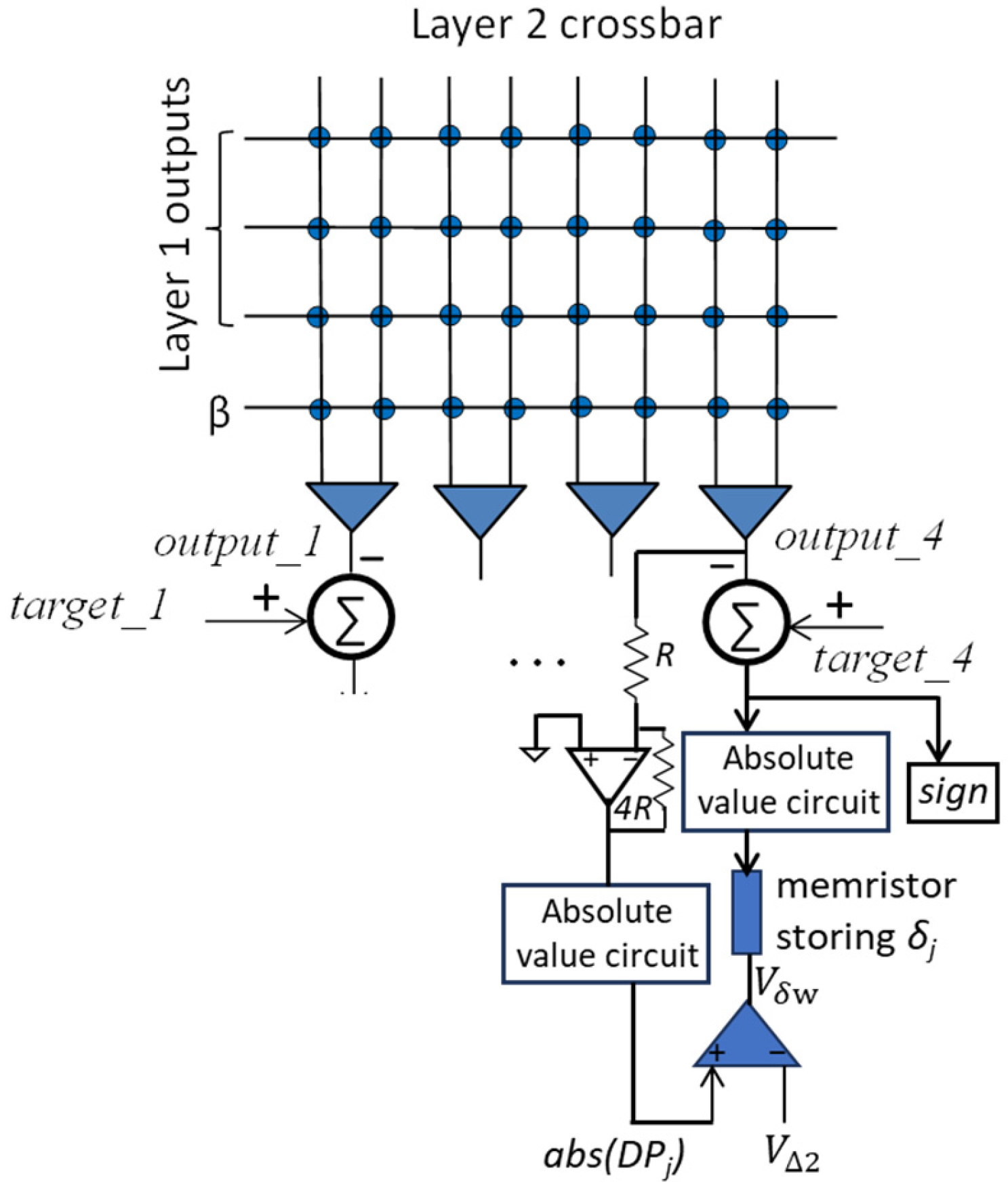
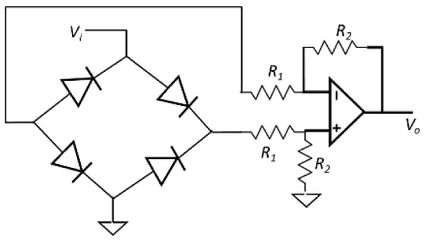
Step 2: The errors of the layer 2 neurons are evaluated according to Equation (4), with the corresponding circuit implementation shown in Figure 9. The magnitudes of the δ j values for the output layer neurons are stored in memristors as changes in conductance. To achieve this, appropriate voltage pulses are applied across the memristor devices, as described in Section 3. In this implementation, (tj yj) determines the pulse amplitude, while dh(DPj) determines the pulse duration. Figure 10 illustrates the waveform VΔ2 used in the Figure 9 circuit. Figure 11 shows the circuit used to evaluate the absolute value of an input voltage. The sign of each error δ j is stored separately in a single-bit memory.
V Δ 2 ( t ) = 4 t T Δ 2                       i f   0 t T Δ 2 / 2 2 4 T Δ 2 t T Δ 2 2       i f   T Δ 2 / 2 < t T Δ 2 0   o t h e r w i s e
Step 3: In the error back-propagation step, the transposed layer 2 weight matrix and the layer 2 neuron errors (δL2,1,…, δL2,4) are multiplied to generate the layer 1 errors (δL1,1 to δL1,3). This operation is shown in Figure 12. If the synaptic weight associated with input i of a layer 2 neuron j is wij = (σij+σij), then the layer 1 errors are calculated as
         δL1,i = (Σjwij δL2,j)f’(DPL1,i) for i = 1, 2, 3 and j = 1, 2, .., 4.
= (Σj(σij+σij)δL2,j)f’(DPL1,i)
  jσij+δL2,j − ΣjσijδL2,j)dh(DPL1,i)
Figure 12 shows the circuit that implements the operations mentioned in Equation (8) for the error back-propagation task. This circuit applies a scaled version of δL2,j and L2,j as input to the layer 2 crossbar columns (j = 1, 2, …, 4). The outputs of this circuit represent the back-propagated errors for layer 1 neurons. The magnitudes of the output errors are also stored in memristors as a change in conductance based on Equation (8). In this case, (Σjσij+δL2,j − ΣjσijδL2,j) determines the write pulse amplitude and dh(DPL1,i) determines the pulse duration. The sign of the error δL1,i is stored separately in a single-bit storage.
Step 4: In a crossbar, synaptic weights are updated neuron by neuron according to Equation (6). In the neuron circuit shown in Figure 1, each synaptic weight is represented by two memristors. When a synaptic weight requires an update of Δw, the memristor connected to Column+ is updated by Δw/2, while the memristor connected to Column− is updated by −Δw/2. The conductance update procedure for Column+ and Column– is the same, except that in Column–, the neuron error term δ j must be multiplied by −1.
Figure 13 illustrates the training pulse generation circuit. The update of synaptic weights depends on four possible cases, determined by the signs of the neuron input xi and the neuron error δ j . Table 3 summarizes these four cases along with the corresponding node potentials in the circuit. The following paragraph explains the training pulse generation technique for case 1.
To update a synaptic weight, a voltage pulse with an appropriate amplitude and duration is applied across the corresponding memristor in the crossbar. The neuron input xi is applied to the row wire connected to the target memristor (see Figure 13). A pulse signal is then applied to the column wire of the same memristor, with its duration modulated by δj. The combined effect of these two signals across the memristor produces a conductance change proportional to δ j × x i . This technique is similar to storing the product of two signals in a memristor device, as discussed in Section 3.
The triangular wave VΔ1 shown in Equation (2) is used to modulate the training pulse duration based on k2 × δj, where k2 is a constant. The duration of this signal, TΔ1 determines the learning rate in the training process. To prevent unintended conductance changes in non-targeted memristor devices, we ensure that |xi| < 2Vth.

5. Experimental Setup

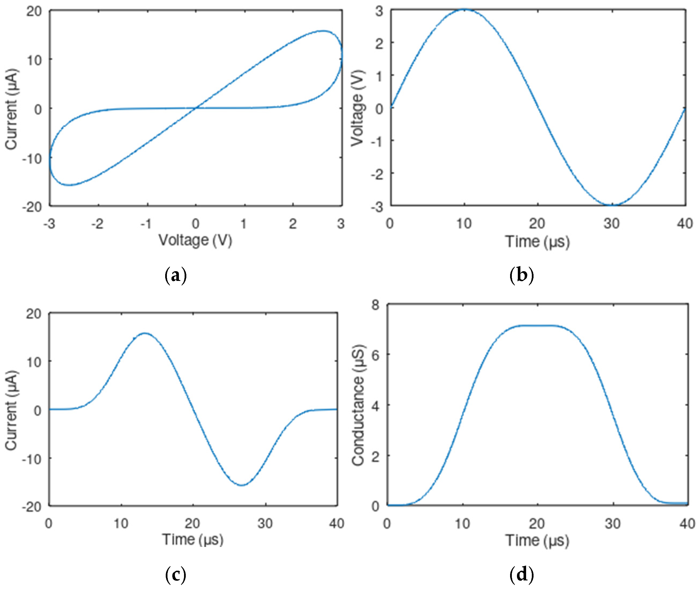
The LTspice tool was used to accurately simulate the memristor grid, taking into account the sneak path currents inherent in the crossbar structure. Each input attribute of the neural network was mapped to a voltage range of [−0.5 V, 0.5 V]. As discussed in Section 4, the duration of the triangular wave, V Δ 1 , determines the learning rate during training. We simulated the memristor device published in [9] using an accurate model of the device published in [30]. The memristor model parameters and the I-V curve are shown in Figure 14. Table 4 summarizes the simulation parameters used for training the MCNNs. The device’s high minimum resistance value helps reduce the circuit’s energy consumption, while its large resistance ratio enables higher weight precision.
We developed a simulation framework using MATLAB R2022a and LTspice IV to implement the training algorithm for MCNNs. LTspice was primarily used for detailed simulations of the memristor crossbar arrays, accounting for sneak path currents, while MATLAB handled the simulation of the remaining system components. The training process was performed iteratively by applying input patterns and updating the synaptic weights until the error was reduced below the desired threshold. We investigated the training of the MCNNs for four nonlinearly separable datasets shown in Table 5. Configurations of the two-layer neural networks used in the experiment are also shown in the table.

6. Results

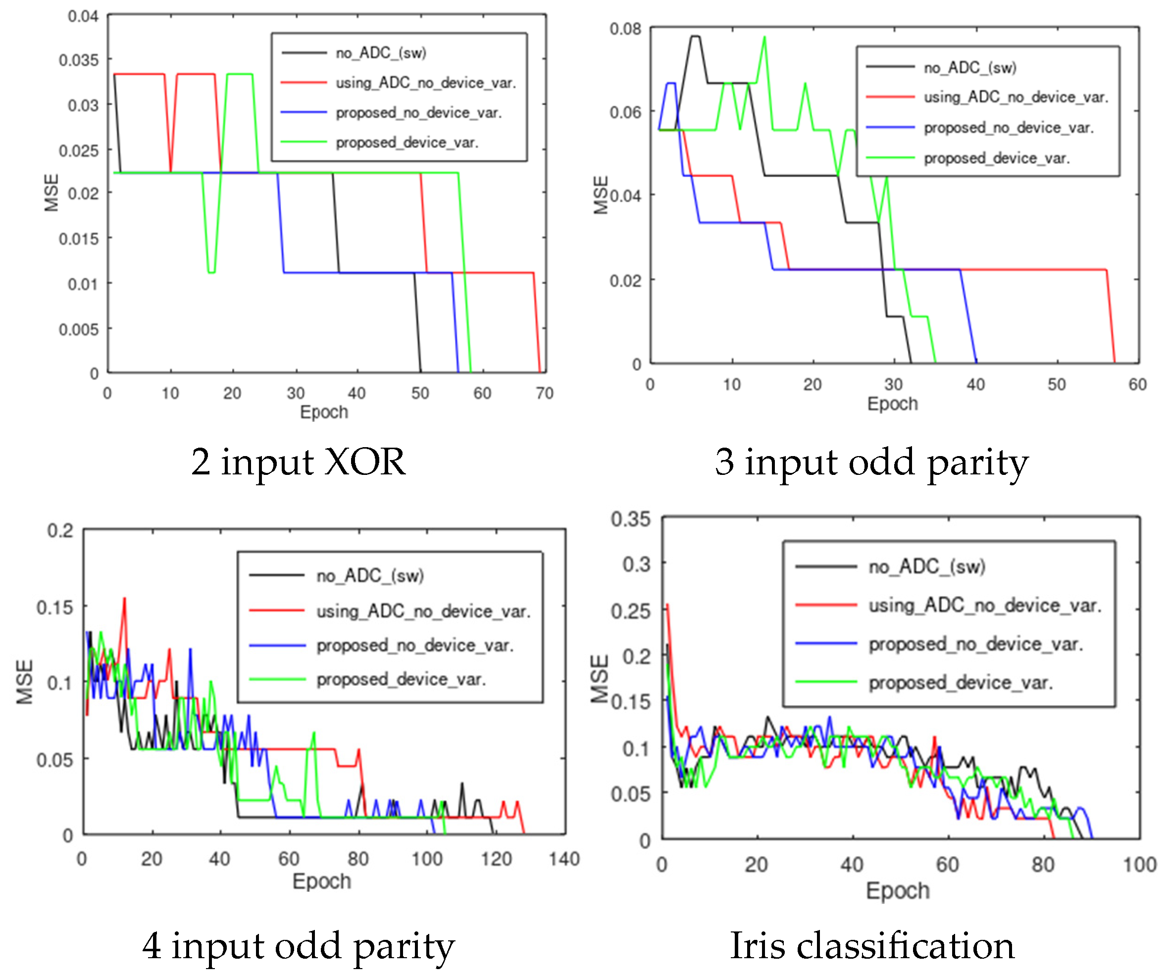
We conducted training experiments on the following memristor-based systems: a system without using ADC (software/floating-point precision), a system with 8-bit ADC/DAC units [13], the proposed system without considering device variation and stochasticity, and the proposed system with device variation and stochasticity taken into account. The training results on various nonlinearly separable datasets are presented in Figure 15. As shown, the neural networks in the proposed system successfully learned the desired separators in both cases, regardless of whether device variation and stochasticity were considered.
The proposed analog on-chip training was performed using a memristor crossbar without ADC quantization. Each memristor cell had an average resistance of 100 kΩ, with 1 ns read and 8 ns write times, consuming 50 fJ and 200 fJ per operation, respectively. The memristor array operated at 2.5 µW average power. Signal processing employed op-amps with 90 ns delay, 3 µW power, and 2.53 µm2 area, consuming 270 fJ per computation. Absolute value circuits were used for nonlinear activation, requiring 400 ns and 0.24 nJ per operation. All computations and updates were performed in the analog domain to minimize data conversion overhead and energy consumption.
Table 6 presents the energy and timing comparison between the proposed system and the system described in [13], which employs 8-bit ADC/DAC units. The results show that the proposed system achieves approximately 2× higher energy efficiency and is about 1.5× faster than the system in [13].

7. Conclusions

This article presents an efficient on-chip training circuit for multi-layer neural networks based on the back-propagation (BP) algorithm. We propose a novel technique for storing the product of two analog signals directly in a memristor device. Unlike previous methods, the proposed approach eliminates the need for costly ADC and DAC converters during training. Experimental results demonstrate that this method achieves faster training and lower energy consumption compared to an existing memristor-based system.

Author Contributions

Conceptualization, R.H.; methodology, R.H., M.S.A. and T.M.T.; software development, R.H. and M.S.A.; investigation, R.H.; formal analysis, R.H.; original draft preparation, R.H.; review and editing, R.H., M.S.A. and T.M.T.; supervision, R.H.; resources, R.H. and T.M.T.; review and editing, R.H., M.S.A. and T.M.T.; project administration, R.H. All authors have read and agreed to the published version of the manuscript.

Funding

This research received no external funding.

Institutional Review Board Statement

Not applicable.

Informed Consent Statement

Not applicable.

Data Availability Statement

Publicly available Iris classification dataset was utilized for this study. Research data will be available upon request.

Conflicts of Interest

The authors declare no conflicts of interest.

Abbreviation

The following abbreviations is used in this manuscript:
MCNNmemristor crossbar-based neural network

References

  1. Kong, L.; Tan, J.; Huang, J.; Chen, G.; Wang, S.; Jin, X.; Zeng, P.; Khan, M.; Das, S.K. Edge-computing-driven internet of things: A survey. ACM Comput. Surv. 2022, 55, 1–41. [Google Scholar] [CrossRef]
  2. Taha, T.M.; Hasan, R.; Yakopcic, C.; McLean, M.R. Exploring the Design Space of Specialized Multicore Neural Processors. In Proceedings of the IEEE International Joint Conference on Neural Networks (IJCNN), Dallas, TX, USA, 4–9 August 2013. [Google Scholar]
  3. Belhadj, B.; Zheng, A.J.L.; Héliot, R.; Temam, O. Continuous real-world inputs can open up alternative accelerator designs. In Proceedings of the 40th Annual International Symposium on Computer Architecture (ISCA), New York, NY, USA, 23–27 June 2013. [Google Scholar]
  4. Zheng, Y.; Yang, H.; Shu, Y.; Jia, Y.; Huang, Z. Optimizing off-chip memory access for deep neural network accelerator. Trans. Circuits Syst. II Express Briefs 2022, 69, 2316–2320. [Google Scholar] [CrossRef]
  5. Chua, L.O. Memristor—The Missing Circuit Element. IEEE Trans. Circuit Theory 1971, 18, 507–519. [Google Scholar] [CrossRef]
  6. Strukov, D.B.; Snider, G.S.; Stewart, D.R.; Williams, R.S. The missing Memristor found. Nature 2008, 453, 80–83. [Google Scholar] [CrossRef]
  7. Ye, L.; Gao, Z.; Fu, J.; Ren, W.; Yang, C.; Wen, J.; Wan, X.; Ren, Q.; Gu, S.; Liu, X.; et al. Overview of memristor-based neural network design and applications. Front. Phys. 2022, 10, 839243. [Google Scholar] [CrossRef]
  8. Aguirre, F.; Sebastian, A.; Le Gallo, M.; Song, W.; Wang, T.; Yang, J.J.; Lu, W.; Chang, M.F.; Ielmini, D.; Yang, Y.; et al. Hardware implementation of memristor-based artificial neural networks. Nat. Commun. 2024, 15, 1974. [Google Scholar] [CrossRef] [PubMed]
  9. Yu, S.; Wu, Y.; Wong, H.-S.P. Investigating the switching dynamics and multilevel capability of bipolar metal oxide resistive switching memory. Appl. Phys. Lett. 2011, 98, 103514. [Google Scholar] [CrossRef]
  10. Medeiros-Ribeiro, G.; Perner, F.; Carter, R.; Abdalla, H.; Pickett, M.D.; Williams, R.S. Lognormal switching times for titanium dioxide bipolar memristors: Origin and resolution. Nanotechnology 2011, 22, 095702. [Google Scholar] [CrossRef]
  11. Le Gallo, M.; Khaddam-Aljameh, R.; Stanisavljevic, M.; Vasilopoulos, A.; Kersting, B.; Dazzi, M.; Karunaratne, G.; Brändli, M.; Singh, A.; Mueller, S.M.; et al. A 64-core mixed-signal in-memory compute chip based on phase-change memory for deep neural network inference. Nat. Electron. 2023, 6, 680–693. [Google Scholar] [CrossRef]
  12. Soudry, D.; Castro, D.D.; Gal, A.; Kolodny, A.; Kvatinsky, S. Memristor-Based Multilayer Neural Networks With Online Gradient Descent Training. IEEE Trans. Neural Netw. Learn. Syst. 2015, 26, 2408–2421. [Google Scholar] [CrossRef]
  13. Hasan, R.; Taha, T.M.; Yakopcic, C. On-chip training of memristor crossbar based multi-layer neural networks. Microelectron. J. 2017, 66, 31–40. [Google Scholar] [CrossRef]
  14. Hasan, R.; Taha, T.M.; Yakopcic, C. A fast training method for memristor crossbar based multi-layer neural networks. Analog. Integr. Circuits Signal Process. 2017, 93, 443–454. [Google Scholar] [CrossRef]
  15. Boquet, G.; Macias, E.; Morell, A.; Serrano, J.; Miranda, E.; Vicario, J.L. Offline training for memristor-based neural networks. In Proceedings of the 2020 28th European Signal Processing Conference (EUSIPCO), Amsterdam, The Netherlands, 18–21 January 2021; pp. 1547–1551. [Google Scholar]
  16. Alibart, F.; Zamanidoost, E.; Strukov, D.B. Pattern classification by memristive crossbar circuits with ex-situ and in-situ training. Nat. Commun. 2013, 4, 2072. [Google Scholar] [CrossRef] [PubMed]
  17. Zhang, X.; Lu, J.; Wang, Z.; Wang, R.; Wei, J.; Shi, T.; Dou, C.; Wu, Z.; Zhu, J.; Shang, D.; et al. Hybrid memristor-CMOS neurons for in-situ learning in fully hardware memristive spiking neural networks. Sci. Bull. 2021, 66, 1624–1633. [Google Scholar] [CrossRef]
  18. Singh, A.; Lee, B.G. Framework for in-memory computing based on memristor and memcapacitor for on-chip training. IEEE Access 2023, 11, 112590–112599. [Google Scholar] [CrossRef]
  19. Shen, S.; Guo, M.; Wang, L.; Duan, S. DTGA: An in-situ training scheme for memristor neural networks with high performance. Appl. Intell. 2025, 55, 167. [Google Scholar] [CrossRef]
  20. Zhang, W.; Yao, P.; Gao, B.; Liu, Q.; Wu, D.; Zhang, Q.; Li, Y.; Qin, Q.; Li, J.; Zhu, Z.; et al. Edge learning using a fully integrated neuro-inspired memristor chip. Science 2023, 381, 1205–1211. [Google Scholar] [CrossRef] [PubMed]
  21. Gao, B.; Zhou, Y.; Zhang, Q.; Zhang, S.; Yao, P.; Xi, Y.; Liu, Q.; Zhao, M.; Zhang, W.; Liu, Z.; et al. Memristor-based analogue computing for brain-inspired sound localization with in situ training. Nat. Commun. 2022, 13, 2026. [Google Scholar] [CrossRef] [PubMed]
  22. Li, B.; Wang, Y.; Wang, Y.Z.; Chen, Y.; Yang, H. Training itself: Mixed-signal training acceleration for memristor-based neural network, Design Automation Conference (ASP-DAC). In Proceedings of the 2014 19th Asia and South Pacific, Singapore, 20–23 January 2014. [Google Scholar]
  23. Fernando, B.R.; Yakopcic, C.; Taha, T.M. 3D memristor crossbar architecture for a multicore neuromorphic system. In Proceedings of the 2020 International Joint Conference on Neural Networks (IJCNN), Glasgow, UK, 19–24 July 2020. [Google Scholar]
  24. Jo, S.H.; Chang, T.; Ebong, I.; Bhadviya, B.B.; Mazumder, P.; Lu, W. Nanoscale memristor device as synapse in neuromorphic systems. Nano Lett. 2010, 10, 1297–1301. [Google Scholar] [CrossRef]
  25. Hu, L.; Yang, J.; Wang, J.; Cheng, P.; Chua, L.O.; Zhuge, F. All-optically controlled memristor for optoelectronic neuromorphic computing. Adv. Funct. Mater. 2021, 31, 2005582. [Google Scholar] [CrossRef]
  26. Xu, G.; Zhang, M.; Mei, T.; Liu, W.; Wang, L.; Xiao, K. Nanofluidic ionic memristors. ACS Nano 2024, 18, 19423–19442. [Google Scholar] [CrossRef] [PubMed]
  27. Yu, S.; Wu, Y.; Jeyasingh, R.; Kuzum, D.; Wong, H.S.P. An electronic synapse device based on metal oxide resistive switching memory for neuromorphic computation. IEEE Trans. Elec. Devices 2011, 58, 2729–2737. [Google Scholar] [CrossRef]
  28. Dong, X.; Xu, C.; Member, S.; Xie, Y.; Jouppi, N.P. NVSim: A Circuit-Level Performance, Energy, and Area Model for Emerging Nonvolatile Memory. IEEE Trans. Comput. Aided Des. Integr. Circuits Syst. 2012, 31, 994–1007. [Google Scholar] [CrossRef]
  29. Qin, F.; Zhang, Y.; Song, H.W.; Lee, S. Enhancing memristor fundamentals through instrumental characterization and understanding reliability issues. Mater. Adv. 2023, 4, 1850–1875. [Google Scholar] [CrossRef]
  30. Yakopcic, C.; Taha, T.M.; Subramanyam, G.; Pino, R.E. Memristor SPICE model and crossbar simulation based on devices with nanosecond switching time. In Proceedings of the 2013 International Joint Conference on Neural Networks (IJCNN), Dallas, TX, USA, 4–9 August 2013; pp. 1–7. [Google Scholar]
  31. Iris Dataset. Available online: https://archive.ics.uci.edu/ml/datasets/Iris (accessed on 1 November 2024).
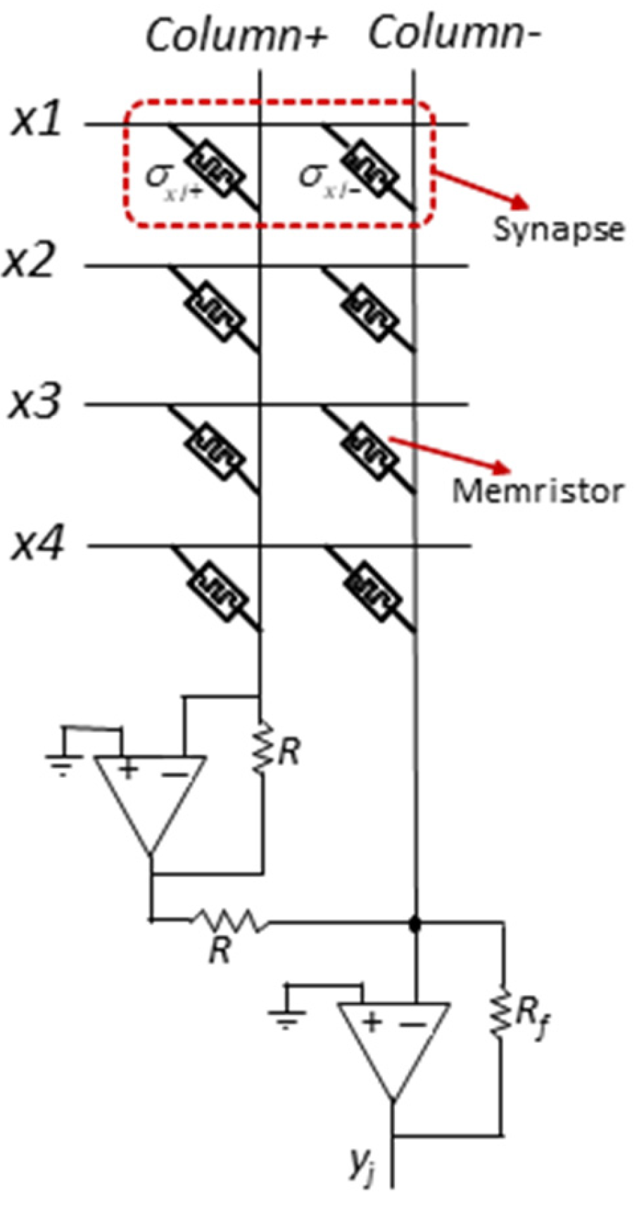
Figure 1. Memristor crossbar-based neuron circuit. Here, x1, x2, x3, and x4 are the neuron inputs and yj is the neuron output.
Chips 04 00038 g001
Figure 2. Graph showing plots of the activation functions f(x) and h(x).
Chips 04 00038 g002
Figure 3. Plots characterizing the memristor device published in [29].
Chips 04 00038 g003
Figure 4. Plot showing the change in conductance with respect to different write voltage amplitudes of the same duration.
Chips 04 00038 g004
Figure 5. Circuit to store the product of two analog voltages in a memristor device.
Chips 04 00038 g005
Figure 6. Plots showing VΔ1,Vy, and Vyw. Here, the duration of Vyw is VyTΔ1 (calculated using the trigonometric formula).
Chips 04 00038 g006
Figure 7. Memristor crossbar-based implementation of a two-layer neural network utilizing the neuron circuit in Figure 1.
Chips 04 00038 g007
Figure 8. Graph showing plots of functions f’(x) and dh(x).
Chips 04 00038 g008
Figure 9. Circuit to generate the output layer error. It takes neuron outputs, corresponding targets, and DPj values of the neurons as input.
Chips 04 00038 g009
Figure 10. Plots showing VΔ2,|DPj|, and Vδw. Here, the duration of Vδw is (1 − |DPj|/2)TΔ2 (calculated using trigonometric formula).
Chips 04 00038 g010
Figure 11. Absolute value generation circuit where Vi is the input voltage and Vo is the output voltage (R2/R1 determines the gain of the circuit).
Chips 04 00038 g011
Figure 12. Schematic of the MCNN shown in Figure 7 for back-propagating errors to layer 1. Here, k1 is a constant.
Chips 04 00038 g012
Figure 13. Training pulse generation module. Inputs to the circuit are mentioned in Case 1 in Table 3. Here, k2 is a constant.
Chips 04 00038 g013
Figure 14. Simulation results displaying (a) the I-V curve, (b) input voltage waveform, (c) output current waveform, and (d) device conductance for the memristor model [30] that was based on the device in [9]. The following parameter values were used in the model to obtain the graphs: Vp = 1.3 V, Vn = 1.3 V, Ap = 5800, An = 5800, xp = 0.9995, xn = 0.9995, αp = 3, αn = 3, a1 = 0.002, a2 = 0.002, b = 0.05, x0 = 0.001.
Chips 04 00038 g014
Figure 15. Training results of MCNNs for four cases: system without using ADCs (software), system using ADCs [13], proposed method without considering memristor device variation, stochasticity (no device var.), and proposed method considering device variation, stochasticity (device var.).
Chips 04 00038 g015
Table 1. Parameters of the memristor device published in [9].
RON (Ω)50 kΩ
ROFF (Ω)10 MΩ
Vth (V)1.3 V
Device switching time for write voltage amplitude 2.5 V20 μs
Table 2. Simulated change in memristor conductance for different pulse amplitudes and durations.
Voltage Across Memristor Device (V)Time (ns)Change in Conductance (S)
1.5351.65 × 10−8
2.5703.46 × 10−7
Table 3. Potential at different nodes of the circuit in Figure 13.
Sign of xjSign of δiWeight UpdateIp1Ip2Ip3VwdVwaiVmemristor = VwaiVwd
For Time TΔ1|δi|Rem. TimeFor time TΔ1|δi|Rem. Time
Case 1++increasexi V Δ 1 i|VthVth|xi||xi| + Vth|xi| − Vth
Case 2+decreasexii| V Δ 1 VthVth−|xi|−(|xi| + Vth)−|xi| + Vth
Case 3+decreasexii| V Δ 1 VthVth−|xi|−(|xi|+Vth)−|xi| + Vth
Case 4increasexi V Δ 1 i|VthVth|xi||xi| + Vth|xi| − Vth
Table 4. Simulation parameters.
Maximum read voltage, Vread0.5 V
Maximum deviation in the response of a memristor device due to device variation and stochasticity30%
Value of the feedback resistance Rf in Figure 1 circuit14 MΩ
Learning rate, TΔ15 ns–8 ns
Table 5. Neural network configurations.
DatasetNeural Network ConfigurationsNumber of Training Data
2 input XOR function3→20→14
3 input odd parity function4→30→18
4 input odd parity function5→40→116
Iris classification [31]5→20→390
Table 6. Energy comparison results for one iteration of the training process.
NN Config.System Using ADC/DAC [13]Proposed System
Time (s)Energy (J)Time (s)Energy (J)
3→20→18.25 × 10−79.32 × 10−117.80 × 10−75.85 × 10−11
4→30→11.01 × 10−61.38 × 10−107.80 × 10−76.18 × 10−11
5→80→11.92 × 10−63.54 × 10−107.80 × 10−71.63 × 10−10
5→15→37.71 × 10−78.13 × 10−117.80 × 10−73.64 × 10−11
Disclaimer/Publisher’s Note: The statements, opinions and data contained in all publications are solely those of the individual author(s) and contributor(s) and not of MDPI and/or the editor(s). MDPI and/or the editor(s) disclaim responsibility for any injury to people or property resulting from any ideas, methods, instructions or products referred to in the content.