Abstract
Artificial intelligence is redefining the computing landscape. Chiplets and heterogeneous integration have become the key strategies for current and next-generation processors. In the wake of Moore’s law slowing down, system integration through advanced packaging has emerged as the leading approach to achieve the highest performance per cost. Overall, the system is converging around substrate which is the main component of packaging. Glass stands out as the superior integration platform for chiplet-based systems. Glass substrates provide unmatched electrical and mechanical properties leading to unprecedented design and integration flexibility at a lower cost than competitive technologies. Three key advantages make glass the platform of choice: the ability to tune material properties, the ability to structure glass, and the feasibility of processing on a large panel scale. This review details the fundamentals of glass processing and manufacturing, innovative integration techniques, and cutting-edge research that collectively position glass substrate as a superior option for the next-generation systems for AI and beyond. Finally, we outline how technology must be shaped in the coming years to drive system scaling.
1. Introduction
The exponential rise in data generation and processing, accelerated by the rapid adoption of generative artificial intelligence (AI), has placed unprecedented demands on computing systems. To sustain this momentum, continuous improvements in system bandwidth are essential. In particular, GPU-memory bandwidth is the main bottleneck for continuous AI improvements. System bandwidth and energy-per-bit are now the main performance metrics due to the need for faster, more efficient data movement across computing architectures. AI needs a lot of memory for training and for storing AI models for inference. Total on-package memory and total memory bandwidth have become key metrics of GPU products from Nvidia and AMD. While high bandwidth memory (HBM) continues to scale with 3D integration of DRAM, GPU to HBM interconnects also need to be scaled to faster bandwidth. Among the primary bottlenecks are interconnects between chips, which now require low-power, high-speed, and high-density on-package wiring solutions. Industry trends show an increasing reliance on substrates and interposers for integrating multiple dies using 2D and 2.5D architectures. Redistribution layer (RDL) interposers and embedded bridges are now central to packaging high-performance devices. Silicon interposers such as TSMC CoWoS and Intel EMIB are two dominant platforms that leverage the back-end-of-line (BEOL) infrastructure to achieve ultra-high I/O density.
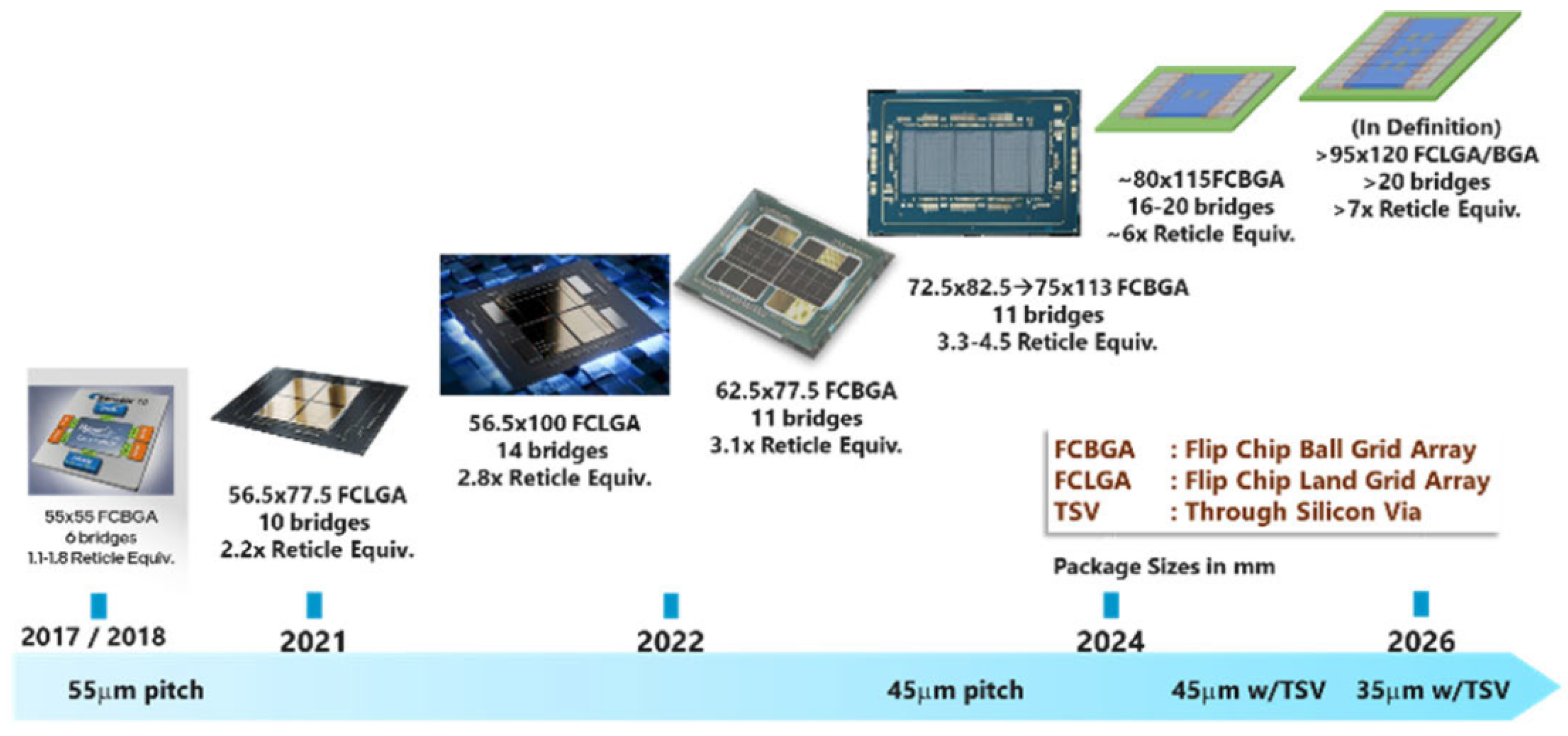
Nvidia’s recent GPUs illustrate the growing need for larger substrates and denser interconnects to support tens of thousands of I/Os and HBM stacks. Figure 1 shows Intel’s roadmap for advanced packaging. With the adoption of the UCIe standard, chiplet integration is poised for rapid expansion. Intel provided a glimpse into the future with their Ponte Vecchio architecture comprising 47 chiplets and 11 EMIB connections [1,2].

Figure 1.
Intel’s roadmap for package form factor and D2D interconnect pitch evolution [2].
The industry is rapidly converging to this modular approach of building an integrated product from a disaggregated system. TSMC recently revealed System-on-Wafer (SoW-X) architecture, having 16 full-reticle-sized ASICs, 80 HBM4 modules, and 100 local silicon interconnect (LSI) bridges. Figure 2 shows the floorplan of SoW-X architecture. This system achieves up to 260 TB/s die-to-die bandwidth and 80 TB/s external bandwidth [3].
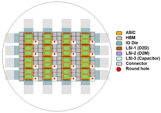
Figure 2.
Floorplan of SoW-X testing vehicle by TSMC [3].
Despite these advances, current approaches face challenges in reliability and scalability. Embedding large numbers of bridges within RDL is assembly-intensive and susceptible to failure from mismatched coefficients of thermal expansion (CTE) between epoxy mold compounds (EMCs) or polymer layers and bridge materials. RDL interposers, while promising for high-density routing, have unproven mechanical robustness at larger package sizes. Shrinkage-induced die shifts during the curing of EMCs, which can exceed 100–200 μm on large wafers, remain a key obstacle in scaling fan-out interposers.
Despite these limitations, glass has emerged as a compelling alternative substrate platform. Its key advantages include the following:
- Tailorable mechanical properties by tuning composition;
- Superior dimensional stability due to its homogeneous structure;
- Compatibility with large-panel manufacturing, leveraging existing infrastructure;
- Enhanced integration capability through microstructuring features like through vias and cavities.
Glass substrates offer a unique combination of silicon’s precision and EMC’s scalability, positioning them as a transformative enabler for future heterogeneous integration. Glass substrates have been shown to deliver significant electrical and manufacturing advantages over silicon and organic counterparts for advanced packaging [4,5,6]. With a low dielectric loss, high resistivity, and stable material properties, through-glass vias (TGVs) achieve >1–2 dB lower insertion loss at 10 GHz than silicon, maintain eye openings >0.6 V with <2 ps jitter over long distances and fast data rates up to 70 Gb/s. TGVs further reduce via-to-via noise coupling by over two times compared to TSVs due to a lower permittivity. Collectively, these results confirm that glass substrates can match or exceed silicon-class interconnect density and electrical performance at lower cost, while supporting panel-scale manufacturing. This review presents the current landscape of glass substrate technologies, covering research innovations, industrial developments, and the path toward commercialization for large-scale, chiplet-based systems using glass as a platform.
2. Current State of the Art
This section describes the current state of development of various technologies, such as through-glass vias (TGVs), glass cavities, fine-pitch RDLs, and reliability.
2.1. Through Glass Vias
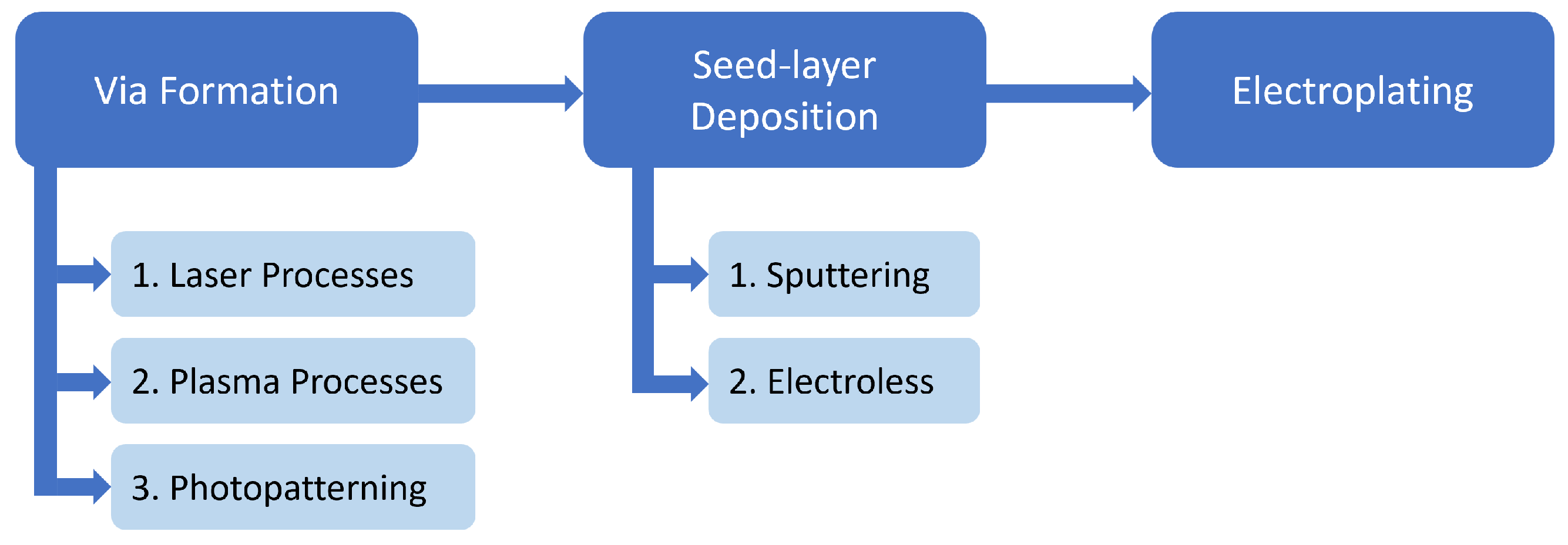
TGVs are fabricated using a sequence of specialized processing techniques, typically divided into two main stages: via formation and metallization. Via formation methods can be broadly classified into three categories: laser-based drilling, plasma-assisted selective etching, and photopatterning in photosensitive glass substrates. Once the vias are formed, metallization is required to establish electrical connections between the top and bottom surfaces of the substrate. Common metallization approaches include sputtering a titanium (Ti)/copper (Cu) seed layer followed by electroplating, electroless copper seed deposition with subsequent electroplating, and direct electroplating. The overall fabrication process is outlined in the flowchart in Figure 3.

Figure 3.
Flow chart showing steps in TGV fabrication.
2.1.1. Via Formation
Laser-based drilling is the most widely adopted technique for forming vias in glass substrates. The choice of laser wavelength is crucial, as it directly influences both the process efficiency and the quality of the resulting vias. Glass absorbs radiation in the deep UV (180–280 nm) and infrared (9.6–10.6 μm) wavelengths [7]. Most of the incident light energy in the infrared regime is converted into lattice vibrations, resulting in material removal through melting and vaporization. At 193 nm, high-energy photons initiate photochemical reactions. This results in the removal of material by breaking chemical bonds within the glass. There are reports indicating that the thermomechanical stresses associated with laser ablation at 193 nm are significantly lower compared to ablation through photothermal interactions at laser wavelength 9.6–10.6 μm [8]. Therefore, excimer lasers at 193 nm are preferred for drilling vias with minimum stress compared to CO2 lasers having a wavelength in the range of 9.6–10 μm [9].
Laser can also be used to locally modify the glass, followed by etching to form vias. This approach is popularly known as Laser Induced Deep Etching (LIDE) and is applied for fabricating small-diameter, high aspect-ratio (AR) TGVs. First, an ultrashort laser with Bessel beam is used to create a laser-affected zone within the glass. In the second step, the modified regions are selectively removed through wet chemical etching, as the laser-affected areas etch at a significantly higher rate than the surrounding glass. One of the limitations of this process is that the via walls are tapered [10,11,12].
To overcome tapered via walls, recent studies have used femtosecond laser modification technology to form laser-affected zone. In this process, either single or burst-mode laser pulses are employed, with precise adjustments to the laser ring size ensuring accurate control of the via diameter across various glass sample volumes. Borosilicate laser-affected zones undergo wet etching using potassium hydroxide (KOH)-based processes, resulting in anisotropic etching, and forming small-diameter, straight, high AR TGVs [13].
Kolari has demonstrated the use of inductively-coupled plasma reactive ion etching (ICP RIE) for the deep (>300 μm) etching of silica and glass with a non-bonded silicon shadow mask. A standard silicon wafer has been used as the shadow mask, and it can be used multiple times. Aspect ratios greater than 3:1 have been achieved with a 400 μm silicon wafer mask by optimizing several parameters, such as the source and bias powers, gas composition, and pressure [14].
Photosensitive glass is patterned using lithographic techniques, in which a mask containing the via pattern is used to expose the glass to UV radiation. This exposure is followed by a thermal treatment that crystallizes the irradiated regions. During etching, the partially crystallized areas exhibit a significantly higher etch rate than the unexposed regions. As a result, these regions can be selectively removed using diluted hydrofluoric acid, revealing the desired via pattern [15].
2.1.2. TGV Metallization
There are two main methods for depositing a seed layer in TGVs: sputtering and electroless deposition. In sputtering, a Ti/Cu seed layer is typically used. Tapered or waisted vias are preferred in this method, as angled sidewalls allow better coverage. However, sputtering has limitations in achieving uniform deposition over large panels and in high-aspect-ratio TGVs. Double-sided sputtering is often needed, increasing the cost. Electroless copper deposition is a lower-cost alternative and is widely used as a standard wet metallization process. This method involves a series of steps which consist of chemical surface treatments, the deposition of catalyst (typically Pd/Sn) particles, and electroless copper reduction on the catalyst particles. This creates three separate, ionic-bonded interfaces between the glass (negatively charged OH-surface), conditioner (positively charged polymer electrolyte), and catalyst (negatively charged surface). Except for the bonding between the Pd catalyst and the electroless-deposited Cu, each of the interfaces between glass and catalyst relies on ionic bonding. Surface etching and roughening are typical parts of electroless plating. These steps improve the adhesion by increasing surface area and mechanical interlocking with the roughened surface [16].
Adhesion between the glass and seed layer is a critical factor for metallization. Both academia and industry proposed several methods to overcome this challenge. Pandey et al. reported localized surface roughening techniques to improve the adhesion of electroless copper in TGVs [17]. Atotech’s Vitrocoat technology achieved a glass-copper peel strength of 4–8 N/cm on a 20–40 nm metal-oxide-based sol gel adhesion promoter deposited via dip coating. The structures passed a highly accelerated stress test (HAST) at 90 % relative humidity, 130 °C for 96 h, and 5× reflow at 260 °C under lead-free reflow conditions. The dip coating mechanism was reported to be successful for TGVs with aspect ratios of up to 5:1 [18]. The TGV blockage due to Vitrocoat GI W can also occur depending on (a) the capillary force of the coating solution, (b) the arrangement of vias, and (c) direction of pull from the dip coating solution. Liu et al demonstrated the dependence of TGV blockage based on the location of the TGV and via pitch in TGV arrays [19].
Xu et al. proposed a mixed metal oxide adhesion layer by incorporating silver nanoparticles on ZnO (SZO) using a sol gel dip coating technique. The adhesion strength was 3–4 N/cm for 11 μm thick electroplated copper for 500 nm adhesion promoter sintered at 500° for 1 h. The silver nanoparticles also provided active catalytic sites needed for electroless copper deposition. TGV fillings with aspect ratios of 1:10 were demonstrated using this approach [20]. The metallization processes, sputtering, and electroless process are generally followed by electroplating for depositing thicker copper layers.
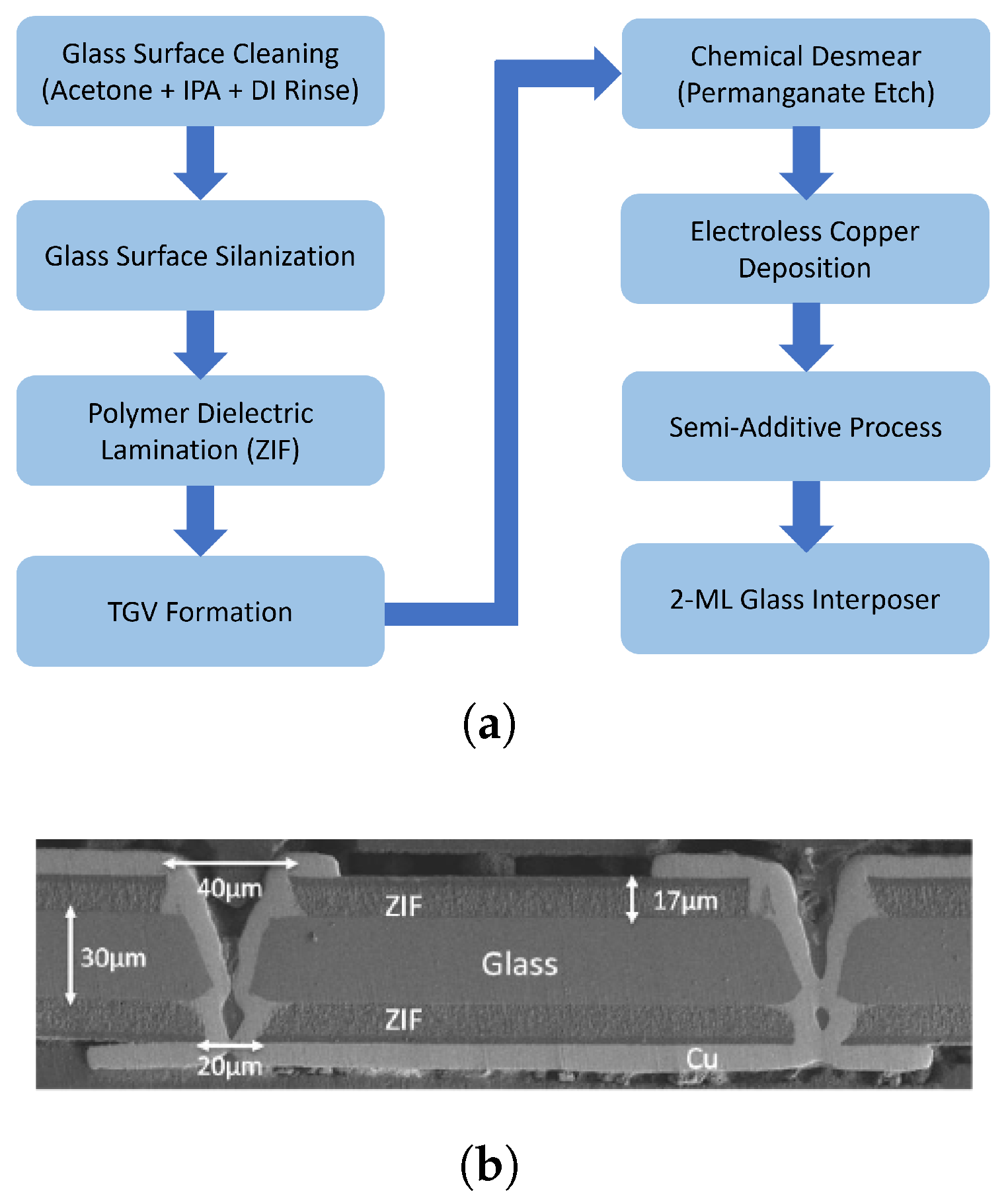
The handling of glass is challenging during the initial processing steps. Laminating a polymer dielectric improves the handling and lowers the chances of breakage. Figure 4a shows the process flow developed by Sukumaran et al. A cross-section image of the interposer formed by this process flow is shown in Figure 4b. It is important to note that a thin film polymer is laminated on glass before drilling vias with laser. This helps in the easier handling of the glass substrate. In this study, excimer lasers at 193 nm were used for drilling vias with minimum stress [9].

Figure 4.
(a) Process flow used by Sukumaran et al. for two-metal-layer glass interposer fabrication. (b) Cross-section image of the interposer fabricated by the given process flow [9].
Pulsed reverse plating is a popular method of electroplating high aspect ratio through holes. In this method, the current is periodically reversed to dissolve surface defects, release trapped gas, and prevent premature via closure, thereby preventing voids. However, pulsed reverse plating is slower than DC plating and requires specialized additives, gantry-style equipment, and unique process parameters that still need further optimization [21]. In a study by Y-H Chang et al., 500 μm thick glass substrates were used, with the TGV entrance and waist diameters of 220 μm and 120 μm, respectively. TGV walls were sputtered with a 0.1 μm thick Ti as an adhesion layer, followed by 1 μm thick Cu as a conductive layer. The glass substrate was subjected to a multistep electroplating process utilizing direct current (DC) at room temperature, where the electric field is perpendicular to the glass substrate. The cross-section image of a via fabricated by this route is shown in Figure 5. The via shown in Figure 5 has a uniform copper thickness (7.7 ± 0.2 μm) at the top, waist, and bottom of the via. This has been achieved by optimizing the current density during the electroplating process [21].
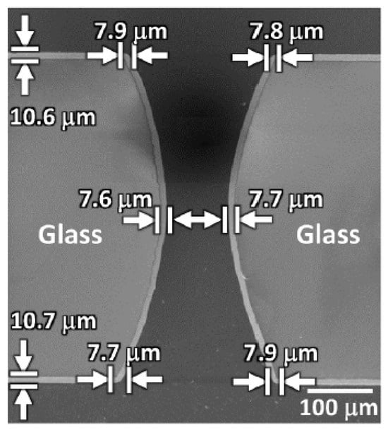
Figure 5.
Cross -section of TGV metallized by Ti/Cu deposition followed by electroplating demonstrated by Y-H Chang et al. [21].
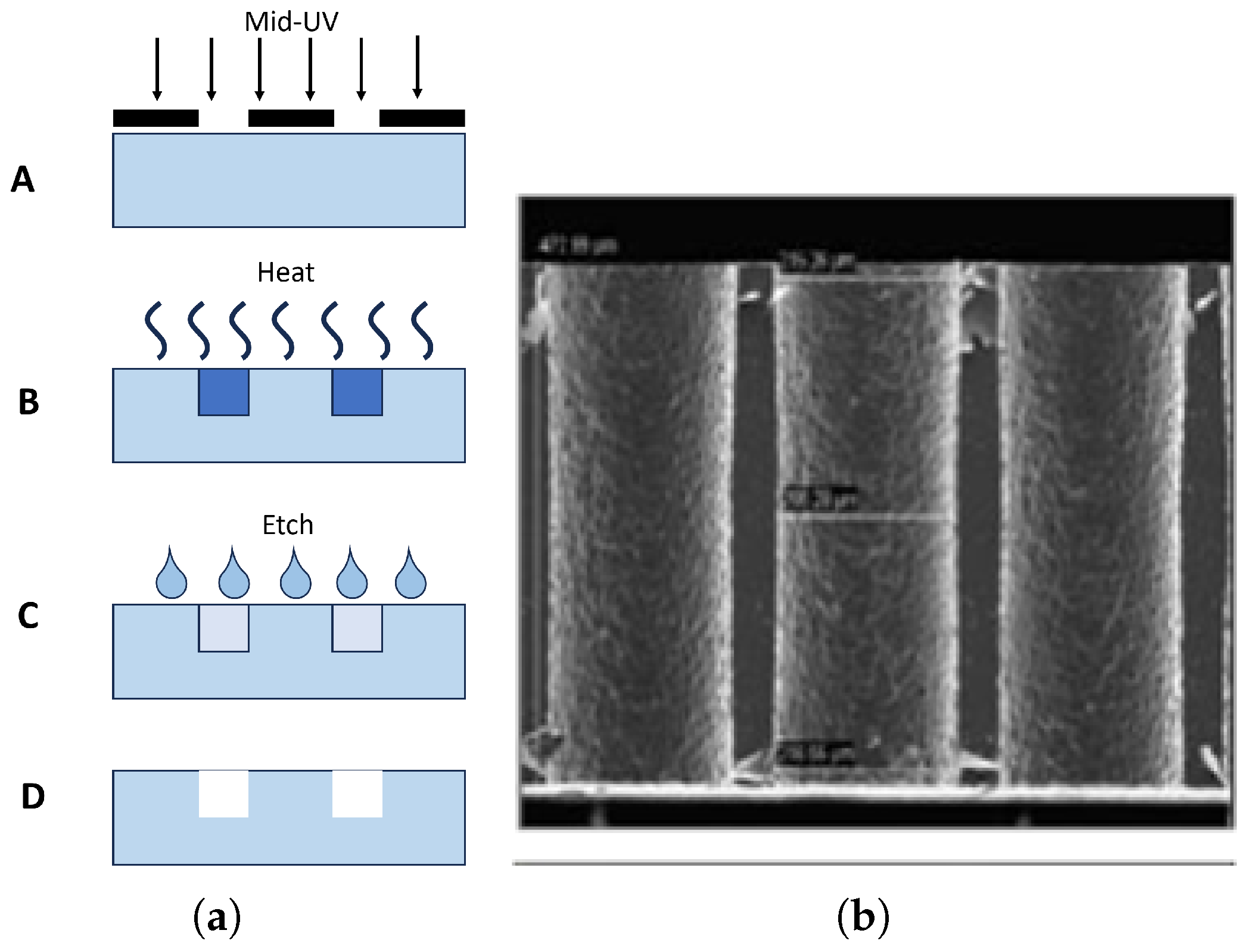
3DGS have demonstrated photopatterned vias with APEX® glass ceramic material. The process flow for via formation with APEX® glass is shown in Figure 6a. The resulting vias, shown in Figure 6b, exhibit a uniform diameter across the entire substrate thickness, with no visible waist or taper. These photo-definable glass ceramic materials are useful for fabricating higher density via arrays with better spatial resolution and improved electrical properties for RF and millimeter-wave frequencies at lower processing costs [22].

Figure 6.
(a) Process flow for APEX® glass ceramic by 3DGS. (b) Vias formed by the given process flow [22].
The conformally pinched via (CPV) approach is a more recent processing route proposed by Kanungo et al. In high-frequency devices or in high-performance displays, it is important to achieve liquid hermeticity and helium hermeticity is often preferred. In these applications, vias need to be completely filled. However, fully filling the vias with copper results in thermomechanical reliability issues due to the large difference in the CTE of glass and Cu. The CPV approach is promising in terms of solving these issues. This approach involves the design of hour-glass shaped vias, followed by the addition of a helium-tight adhesion layer to the sidewalls near via entry. This is followed by superconformal plating inside TGVs using Nitro Tetrazolium Blue Chloride Monohydrate (NTBC) as an additive in the plating bath, which results in defect-free bridging at the center of the vias [23]. An X-ray computed tomography (CT) image of vias metallized by this approach is shown in Figure 7.

Figure 7.
X-ray CT image of conformally pinched vias demonstrated by Kanungo et al. [23].
2.1.3. Commercial TGV Capabilities
Although numerous academic studies have addressed TGV formation and metallization, scaling these processes for high-volume manufacturing remains a significant challenge due to the stringent demands for repeatability and reliability. Key manufacturing targets include achieving smaller via diameters, a finer pitch, and high aspect ratios on large wafers and panels. AGC is capable of fabricating TGVs with diameters ranging from 20 μm to 150 μm and minimum pitcher sizes twice the via diameter. They utilize EN-A1 non-alkali glass in wafer sizes up to 300 mm and panel sizes up to 550 mm × 650 mm, with glass thicknesses between 0.1 mm and 0.5 mm [24]. Corning has comparable TGV fabrication capabilities. They are capable of fabricating TGVs having a diameter of 30 to 100 μm and a minimum pitch twice the diameter on wafers of 300 mm diameter and panel dimensions of 515 mm × 515 mm [25]. 3DGS manufactures TGVs with diameters down to 30 μm and aspect ratios up to 10:1. They can achieve an edge-to-edge distance as small as 10 μm between the TGVs using APEX® Glass [26].
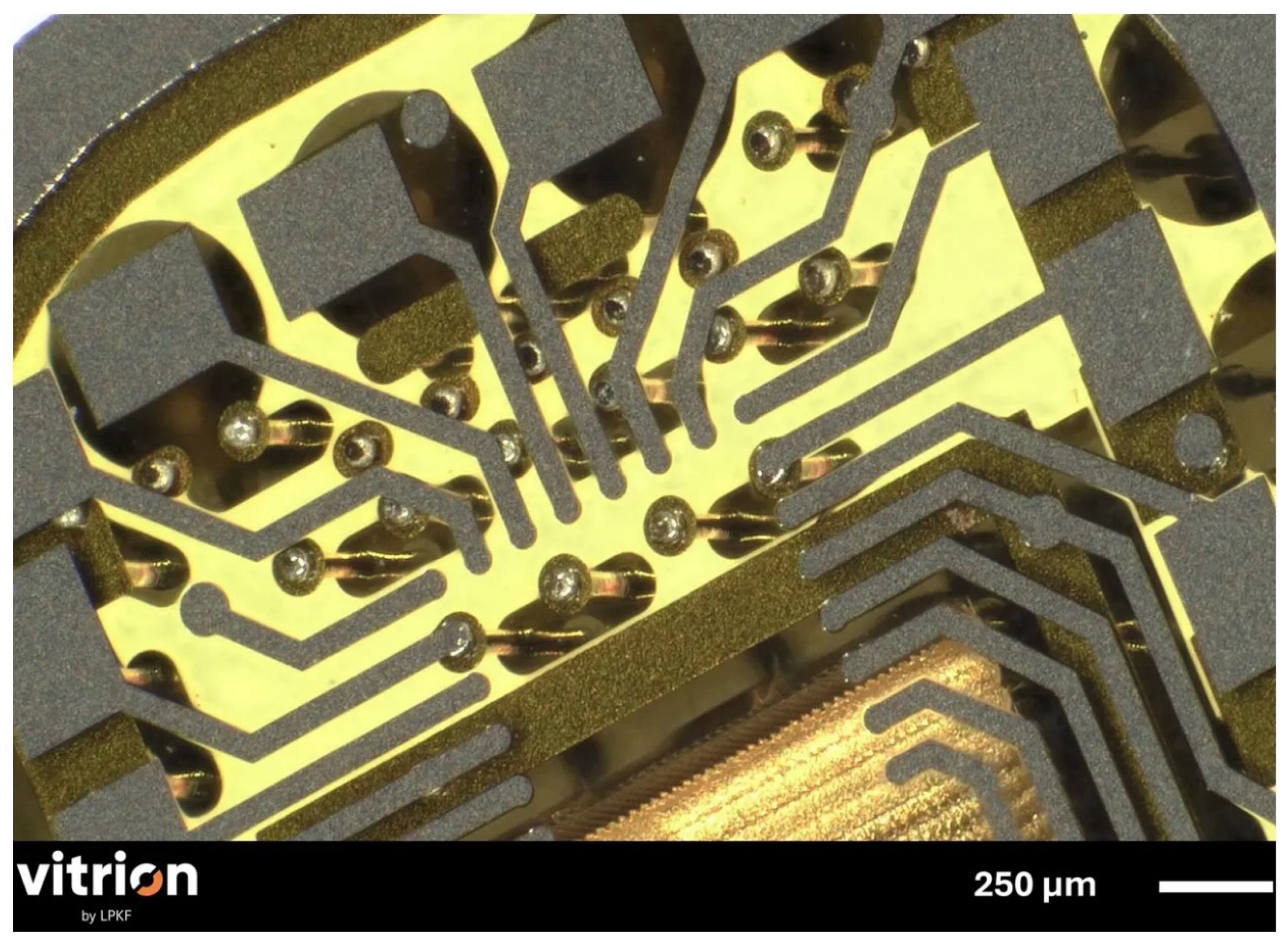
Vitrion uses LIDE® (Laser Induced Deep Etching) technology for TGV fabrication which enables precise microstructuring of glass without mechanical damage or residual stress. This process helps Vitrion achieve vias with high aspect ratios of up to 50:1 and sub-micrometer accuracy. The process is versatile since LIDE® is not limited to specific glass types [27]. A typical three-layer glass package with TGVs, signal lines, and solder balls fabricated by Vitrion is shown in Figure 8. Planoptik fabricates straight, tapered or hourglass-shaped TGVs having a minimum diameter of 50 μm by a bulk micromachining process on glass and quartz wafers. The wafer diameters can be up to 300 mm and the thickness ranges from 200 μm to 2 mm [28].

Figure 8.
Typical three-layer glass package with TGVs, fabricated by Vitrion [29].
NSC Co., Ltd. fabricates TGVs with aspect ratios up to 10:1. The via diameters range from 20 μm to over 1 mm. They are capable of fabricating vias at extremely tight pitch sizes that marginally (10%) exceed the via diameter with a tolerance of ±15 μm. They process various glass types, including non-alkali, alkali, quartz, and heat-resistant glass, with thicknesses from 0.05 mm to 1.65 mm. The maximum size of glass panels that they can process is 730 mm × 920 mm [30]. Dai Nippon Printing (DNP) has the capability to fabricate glass substrates with TGVs exhibiting aspect ratios exceeding 9:1. Their conformal-type TGVs feature metal layers adhered to via-sidewalls, enhancing adhesion and reliability for fine wiring configurations. DNP is also promoting the scalability of the conformal-type TGVs to a panel size of 510 mm × 515 mm [31]. Tecnisco Ltd. fabricates TGVs with minimum diameters of 150 μm and aspect ratios up to 5:1, using borosilicate glasses like Borofloat 33 and SW-YY. Their processes accommodate glass wafers of 200 mm diameter and thicknesses as low as 0.3 mm [32].
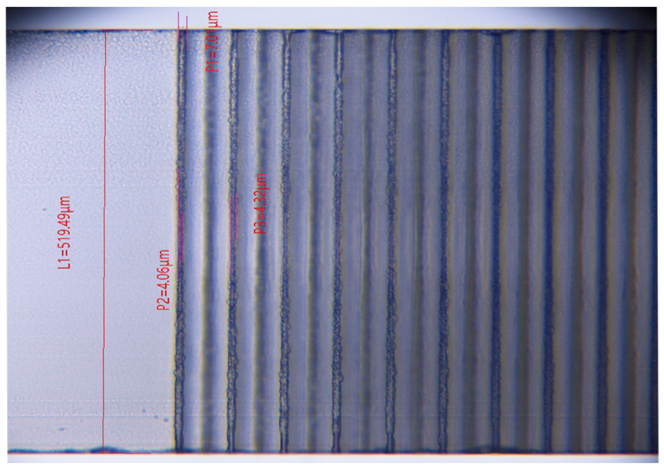
Shanghai Famous Trade Co., Ltd. (ZMSH) fabricates TGV substrates with via diameters as small as 3 μm and pitches approximately twice the via diameter. Their glass thicknesses range from as low as 50 μm to under 0.7 mm. They utilize high-quality borosilicate glass and fused quartz, suitable for applications requiring high-density interconnections and low-loss transmission. They are capable of processing a maximum wafer size of 8”, and panel size of 510 mm × 510 mm [33]. Xiamen Sky-semi Microelectronics Co., Ltd. (Xiamen, China) has demonstrated advanced TGV capabilities, achieving ultra-high aspect ratios ranging from 20:1 to 100:1. Their TGV structures include cylindrical, trapezoidal, and slot-shaped vias, suitable for high-density interconnects in MEMS and RF applications. Xiamen Sky-semi Microelectronics uses laser-assisted etching techniques to fabricate these vias in various types of glass substrates, such as borosilicate and fused silica. The minimum via diameter and pitch that they can achieve are 5 μm and 10 μm, respectively. The use of laser assisted techniques help in the precise control of via geometry and pitch [34]. Figure 9 shows 10 μm vias on 500 μm thick glass fabricated by these techniques. Lante Optics provides TGV solutions with via diameters down to 20 μm, pitches in the range of 50 μm to 150 μm, and aspect ratios up to 10:1. They use materials like fused silica and can work with wafer sizes of up to 12” diameter [35].

Figure 9.
High aspect ratio (520:7) TGVs fabricated by Xiamen Sky-semi Microelectronics [34].
2.2. Formation of Glass Cavities and Embedding
Multiple methods are reported in the literature for structuring or making cavities in glass. Wet etching is the most common process that involves submerging the glass panel with an attached mask into hydrofluoric acid (HF), dissolving the vitreous silicate [36]. The etching rate depends on the concentration of HF and the etching is isotropic. Proper mask design and material selection are critical for defect-free deep glass etching. Iliescu et al. investigated defect formation during the wet etching of Pyrex glass and identified key factors that influenced etch quality and depth. Optimal etching was achieved using low-stress multilayer masks, hydrophobic surfaces, and high-concentration HF or HF/hydrochloric acid (HCl) mixtures. Etch rates up to 7.5 μm/min and depths exceeding 1 mm were demonstrated with minimal roughness [37].
In dry etching, also known as reactive ion etching (RIE), the patterned glass panel is exposed to a plasma of reactive gases such as SF6 and Ar [38]. The ions from these gases strike the substrate and etch the material [39]. Power, gas flow rate, and pressure play a role in determining the etching rate. Unlike wet etching, dry etching is anisotropic and this results in a good sidewall profile. However, this technique is limited by a slow etching rate (typically less than 1 μm/min) which necessitates an hours-long process duration for typical glass thicknesses of 100–500 μm [40]. Selectivity is an important parameter that determines the quality of etching. Poor selectivity can cause more damage to the glass substrate. The etching method and the mask material are crucial for a high-yield process; for example, the selectivity of dry etching ranges from 3.9 to 23 [40].
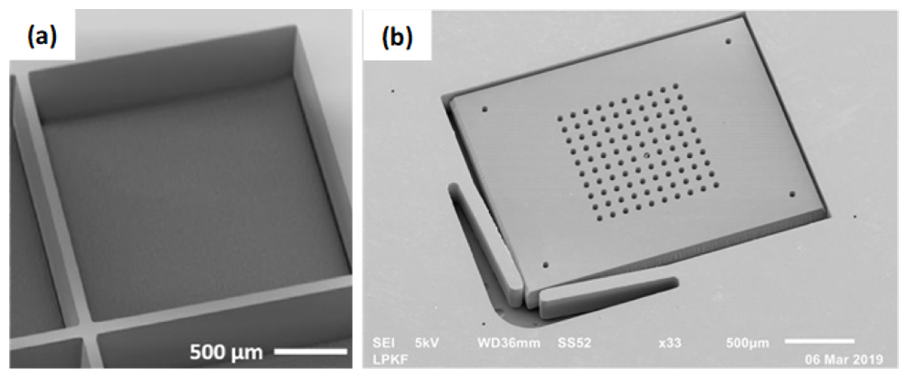
Laser ablation is an alternative method for fabricating glass cavities. Fine control over cavity dimensions and positions is possible by adjusting parameters such as pulse duration, laser power, and focus. However, high-energy pulses result in superficial and internal defects such as cracks. LIDE has been shown to be a superior option compared to conventional laser processing. Santos et al. demonstrated LIDE as a breakthrough method for fabricating defect-free, high-precision cavities in glass. A novel passive die alignment mechanism shown in Figure 10 achieved 4 μm accuracy [12].

Figure 10.
(a) Blind cavity with controlled depth. (b) Scanning electron microscope (SEM) micrograph of a die in a glass cavity with passive alignment features [12].
Glass, when used for die embedding, not only surpasses organic alternatives but also offers several unique advantages over current wafer-level fan-out (WLFO) technologies. Its smooth surface and high dimensional stability support an unmatched combination of high I/O counts and scalability that mold compound-based fan-out cannot achieve. The chip-first process is the most common for embedding in glass cavities depicted in Figure 11 [41]. First, glass panels with cavities are mounted on a carrier using temporary thermal release tapes. The dies are placed into the cavities using a flip-chip bonder. Next, the first dielectric film is laminated on the top side of the substrate. After curing, the dielectric film flows and fills the gaps between the dies and the glass substrate, resulting in the dies being encapsulated inside the cavity. The through cavity requires a temporary carrier on the bottom to support the chip. The major advantage of glass over epoxy mold compound is reduced die shift. Mold compound needs to be cured over the whole wafer or panel area, leading to shrinkage and distortions that cause die shifts of >100 μm [42]. Meanwhile, in the case of glass embedding, curing of the polymer is localized to the cavity regions. Ravichandran et al. developed and optimized the process flow to achieve a die shift of less than 2 microns. Die shifts in cavity were reduced from 25–30 μm to less than 2 μm by the use of a die attach film and two-step curing process [43,44]. Lower die-shifts enable smaller capture pads, leading to higher wiring density than traditional fan-out packages.
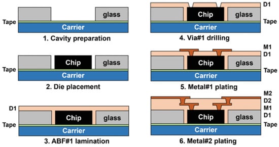
Figure 11.
Process flow for chip embedding and RDL formation [41].
2.3. Fine Line RDL on Glass
Glass has numerous advantages over conventional organic laminates for fine-line patterning. The ultra-low roughness (Ra < 1 nm) of glass is advantageous in minimizing diffused reflections at the copper seedlayer–photoresist interface, thus enabling very fine lithographic dimensions. Furthermore, the tunable coefficient of thermal expansion (CTE) of glass can be used to minimize the warpage of the substrate, enabling ultra-high IO density multilayer RDL packages. Glass also provides a very low thickness variation, which makes it easier to focus uniformly, over a large panel area, during the lithography process.
The Georgia Tech Packaging Research Center has carried out significant research in fine-line RDL on glass substrates. Key challenges in fine-line RDL fabrication include lithography and seed etch processes. Lu et al. demonstrated an advanced semi-additive process (SAP) to fabricate 2–5 μm RDL traces on thin, panel-based glass interposers, enabling high-density chip-to-chip interconnects for 2.5D systems. A differential copper seed layer etching method was used [45].
Liu et al. have reported extensively on photoresist and lithography processes to achieve 1 μm linewidth over large panels [46]. In one of our previous reports, a novel low-cost “etch barrier” technique was developed to prevent lateral etching of copper traces in semi-additive processing (SAP) for package RDL. A 50 nm titanium sidewall barrier protecting RDL traces during wet seed-layer etching enabled precise control without trace narrowing. The process achieved line/space dimensions as low as 1/1 μm and even 2.5/0.5 μm using standard SAP tools [47].
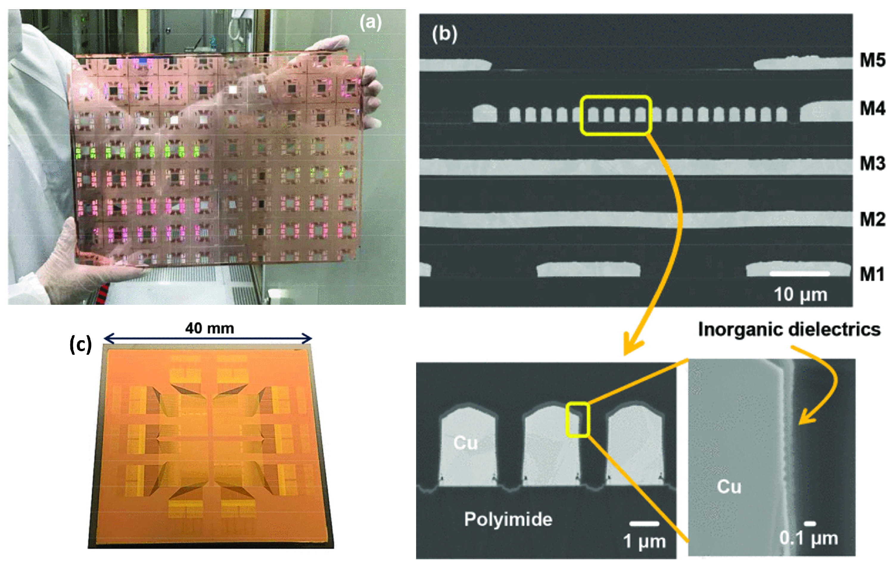
Kudo et al. at DNP presented a large panel-scale RDL interposer fabricated on 300 mm × 400 mm glass panels using a 2 μm pitch semi-additive process. This is shown in Figure 12. Dry plasma etching was used for seed etch, forming 1 μm wide copper traces having high aspect ratios (>3) and no trace-width changes. The traces were covered with inorganic dielectrics for reliability [48].

Figure 12.
(a) DNP’s RDL on 300 mm × 400 mm glass panel. (b) SEM cross-section of Cu traces (c) Glass Interposer [48].
2.4. Reliability Studies
Discontinuities are the most frequent failure points across all types of electronic packages. For glass substrates in particular, the most critical areas are the through-glass vias (TGVs) and the ball grid array (BGA) interfaces.
2.4.1. TGV Reliability
Vias are one of the most common failure points in packages. TGV reliability has been an important area of research since the advent of glass substrates. The inherent mismatch in the physical properties of copper and glass has led to reliability challenges. Various parameters like the TGV diameter, pitch, glass composition, stress relieving mechanisms, process parameters, and TGV geometries have been investigated. Demir et al. investigated the thermomechanical reliability of copper-filled TGVs in 100 μm thick glass with 30 μm vias at 120 μm pitch. Simulations in the temperature range of −55 °C to 125 °C showed that the expansion and contraction of copper generate radial and shear stresses at the glass interface, potentially causing cracks. Larger pitches reduced neighboring via stress interactions, and parametric analysis revealed that the TGV pitch ≥2X via diameter minimized neighboring stress interaction. A TGV pitch four times the via diameter was selected for fabrication. Structures withstood 3000 thermal cycles with stable DC resistance. While no copper cracks were observed, delamination and glass cracks confirmed failure zones predicted by stress simulations [49].
Various solutions have been proposed for reducing the stress at the glass–copper interface. Ahmed et al. reported stress buffer layers as a solution to improve the reliability of TGVs by mitigating substrate cracking caused by thermal expansion mismatch between copper vias and glass. High-temperature processes like annealing can induce tensile stresses at the via–glass interface, initiating radial cracks. Introducing a thin, compliant polymer liner significantly reduces these stresses. Finite element simulations showed >75% reduction in energy release rate compared to solid vias, lowering crack risk [50].
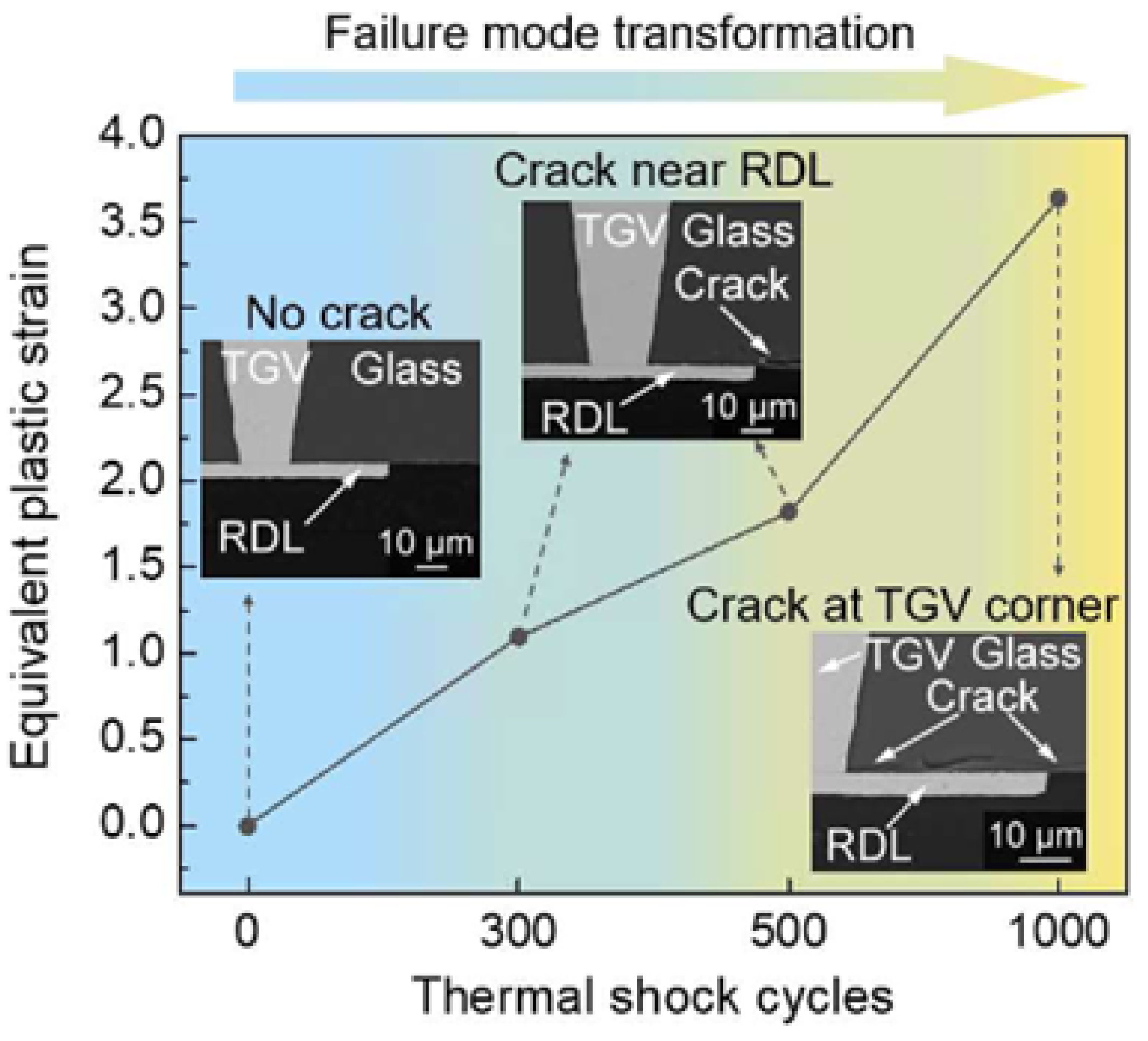
Pan et al. investigated the thermomechanical behavior of copper-filled TGVs under thermal cycling using in situ measurements and simulations. The protrusion of copper increased with slower temperature ramp rates, with irreversible deformation (∼1.3 μm at 400 °C) caused by creep. In-plane glass deformation peaked near 250 °C and was largest at via edges. Slower ramp rates reduced glass displacement and stress. Simulations confirmed critical stress zones near the copper–glass interface, validating the importance of ramp-rate control for TGV reliability [51]. Wang et al. studied the failure modes of copper-filled TGVs inspected during thermal shock. Glass cracking was observed after 300 cycles near TGV-RDL at the top and bottom edge of the samples. During thermal shock, glass cracking was proposed due to internal stress on glass, when subjected to quick compression and stretching cycles in axial and radial directions. As cycles increased to 1000, cracking was found near the TGV. Figure 13 shows equivalent plastic strain as a function of thermal shock cycles [52].

Figure 13.
Equivalent plastic strain as a function of thermal shock cycles [52].
Various TGV formation processes lead to different TGV geometries that have an impact on reliability. Fujimoto et al. investigated different TGV geometries for stress and reliability. Straight and X-shaped TGVs (AR = 12) were studied for thermal stress analysis, based on the temperature rise of the glass core. X-shaped vias were found to handle more thermal stress because of the higher via angle. Thermal cycling experiments were conducted. No significant resistance change was observed even after 1000 thermal cycles for all three types of via filling methods (fully, partially, and conformally filled vias) [53].
Leakage and moisture absorption often limit the reliability of traditional substrates, whereas glass’s inherent hermeticity offers significantly improved reliability. Okoro et al. assessed helium hermeticity of copper-filled TGVs in Corning HPFS glass under thermal shock, high-temperature storage (HTS), and highly accelerated stress testing (HAST). All samples exceeded requirements, surviving up to 9000 thermal cycles and 4600 h HTS without leaks. HAST caused failures after 400–1600 h due to Cu oxidation (CuO/Cu2O) and Ti–Cu interface debonding. Overall, Cu TGVs showed high reliability for stringent hermeticity applications [54].
2.4.2. BGA Reliability
Glass offers controllable CTE that allows matching to silicon chips or the organic board. There are detailed studies on microbump versus BGA reliability using glass substrates. Multiple reports agree that matching the CTE of glass to the PCB is more important. Lau et al. studied solder reliability at microbumps, and controlled collapse chip connection (C4) joints for organic and inorganic packages. Thermal cycling was carried out between −40 and 85 °C with a dwell time of 15 min each. Glass substrates exhibit larger deformation than organic substrates on thermal cycling (both heating and cooling cycles) because of higher CTE mismatch with PCB. However, the maximum accumulated equivalent inelastic strain in the microbump is smaller in the case of glass package. This was attributed to a smaller CTE mismatch between glass and chip. The authors observed that since solder joints at the PCB level seldom have underfill (unlike microbumps at the chip level) it is more important to match the CTE of the package with PCB rather than the chip in this case. This is also because the maximum accumulated equivalent inelastic strain in the C4 solder bump is more than two times larger in the case of glass package. However, since glass has tunable CTE, the selection of glass CTE close to PCB will greatly reduce deformation in large glass panels [55].
Jayaram et al. presented a design and simulation framework to optimize thermomechanical reliability and warpage in large 2.5D glass BGA packages. Using finite element analysis (FEA) in ANSYS, the study evaluated chip and board-level fatigue life and warpage behavior for glass-based BGA packages with sizes of 30 mm × 40 mm and 40 mm × 50 mm. The modeled structure was initially subjected to a temperature drop from 260 °C to 25 °C to simulate the cooling phase of the SMT reflow process. Subsequent thermal cycling followed the JEDEC standard JESD22-A106B [56] involving five cycles between −40 °C and 125 °C to assess fatigue performance. Substrates with CTE values of 3 and 9.8 ppm/°C were examined, using SAC105 solder for chip and board-level interconnections. Fatigue life predictions were based on Coffin–Manson and Engelmaier–Wild models as shown in Figure 14, and warpage-induced yield risks were evaluated according to JEITA standards. The equivalent plastic strain in the corner solder joint was observed to stabilize after five thermal cycles. One of the key takeaways is that high-CTE glass improves board-level reliability by reducing solder strain but significantly increases chip-level warpage, which can cause yield loss. In contrast, low-CTE glass reduces warpage but does not meet board-level reliability requirements. For 30 mm × 40 mm packages, an optimal CTE range of 5–7.5 ppm/°C was identified to balance both criteria. Larger packages have narrower design windows and are more prone to trade-offs [57].
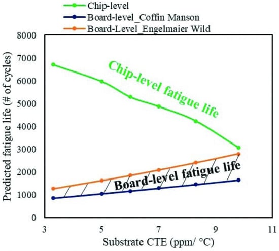
Figure 14.
Prediction of fatigue life at chip level and board level for various glass CTE values [57].
Different solder material types can also be used to optimize the BGA reliability of glass substrates. In another article, Jayaram et al. investigated the reliability of single-chip glass BGA packages with a focus on standard BGA solder balling using SAC105, SAC305, and Mn-doped SACm alloys for direct attachment to the board. A parametric finite element analysis evaluated the impact of glass CTE (3.3 and 9.8 ppm/K) on fatigue life at board level. Experimental thermal cycling (–40 °C to 125 °C) validated model predictions, with SACm achieving similar reliability to SAC305 and outperforming SAC105. Notably, the addition of polymer collars around solder balls further improved fatigue life by ∼25%, mitigating warpage-induced early failures seen in low-CTE samples. All configurations passed the 1000-cycle JEDEC standard, but high-CTE packages demonstrated extended life beyond 2600 cycles, suggesting better scalability for advanced, larger packages. The study confirms that combining high-CTE glass, Mn-doped solders, and polymer collars presents a promising path toward reliable, thin, large-area glass BGA packages [58].
Singh et al. presented the first demonstration of both thermal cycling and drop-test reliability for large, ultrathin glass BGA packages (18.5 mm × 18.5 mm, 100 μm thick) directly mounted onto PCBs via SMT, without intermediate organic packages. Low-CTE samples failed after 1100 cycles, while high-CTE samples exceeded 5000 cycles with stable performance. Failure analysis revealed fatigue cracks originating at the solder/glass interface, consistent with areas of high plastic strain. Drop-test results following JESD22-B111 standard [59] showed that 28 out of 30 samples met the criteria, with no significant influence of glass CTE on drop reliability. Predominant failure modes included copper trace fractures and interfacial cracks near the Ni/Cu interface, often related to fabrication cleanliness. Crucially, no glass cracking or delamination was observed, demonstrating that with proper edge protection and process control, glass substrates can be robust under mechanical stress [60].
3. Architectures and Novel Integration Approaches
3.1. Glass Panel Embedding (GPE)
Glass Panel Embedding has emerged as a promising advancement in the domain of high-density packaging, enabling heterogeneous integration through die embedding within structured glass substrates. Building on prior work in glass-based interposers, GPE leverages the unique properties of glass such as its low loss characteristics, dimensional stability, and tailorable coefficient of thermal expansion (CTE), while introducing a panel-scale embedding approach that eliminates the reliance on Through Silicon Vias (TSVs) or mold compound encapsulants. In contrast to TSV-based 2.5D and 3D silicon interposers, where vertical connectivity is achieved by etching through silicon wafers at significant cost and process complexity, GPE allows for passive integration of known good dies into glass cavities, with signal and power redistribution implemented through multilayer polymer redistribution layers.
Unlike wafer-level fan-out packages, which are limited by warpage and mold stability at finer pitches, GPE offers a thermomechanically robust substrate that supports fine pitch IO (<20 μm), higher wiring densities, and large area panel format. The use of glass also enables reduced warpage and superior surface planarity, which are critical for fine line lithography and multi-die assembly. Additionally, GPE eliminates many of the limitations associated with bump reflow and warpage control in organic packages and avoids the die yield penalties associated with preassembled TSV-based stacking.
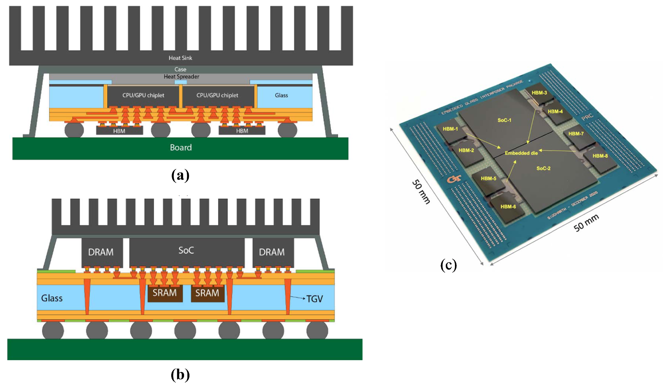
Generic process flow for Glass Panel Embedding was discussed in the earlier section [41]. Based on specific architecture, the process flow may vary and can be more intricate. The GPE process is fully compatible with standard OSAT assembly workflows, enabling the seamless integration of dies from multiple process nodes and foundries. GPE packages achieve <2 μm die shifts, which enable chip-first, multi-die, high-density 2.5D packages. The lower die shifts reduce the required pad sizes, thereby increasing the routing density. Dies can be placed side by side at <100 μm spacing, enabling bandwidth densities exceeding 1 TBps. S. Ravichandran et al. [44] reported the demonstration of two glass-based 3D package architectures enabled by GPE for high-performance computing applications. Figure 15a,b show the schematics of these two architectures. In this approach, dies were embedded within glass cavities and interconnected using polymer-based redistribution layers (RDL), thereby eliminating the need for TSVs. In the first test vehicle, two dies were laterally embedded within a glass cavity with a die-to-die spacing of approximately 92 μm and interconnected through 16 μm microvias. Additional HBM emulator dies were assembled on top using microbumps, achieving vertical interconnect lengths of less than 45 μm. The IO pitch was scaled to below 20 μm, enabling high-density integration. In the second vehicle, a 50 mm × 50 mm glass interposer was used to embed four dies beneath two large SoCs and eight HBM emulator dies mounted on the surface at 35 μm bump pitch. Plated TGVs with 300 μm pitch were used for board-level connectivity, and thermal management was optimized by avoiding the embedding of high-power dies. These architectures were fabricated on panel-scale substrates and demonstrated the scalability, fine-pitch capability, and thermal advantages of GPE as a TSV-free platform for heterogeneous integration in advanced computing systems.
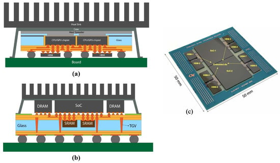
Figure 15.
(a,b) Different architectures with chips embedded in glass (c) Embedded Glass Interposer Package after assembly and capillary underfill [44].
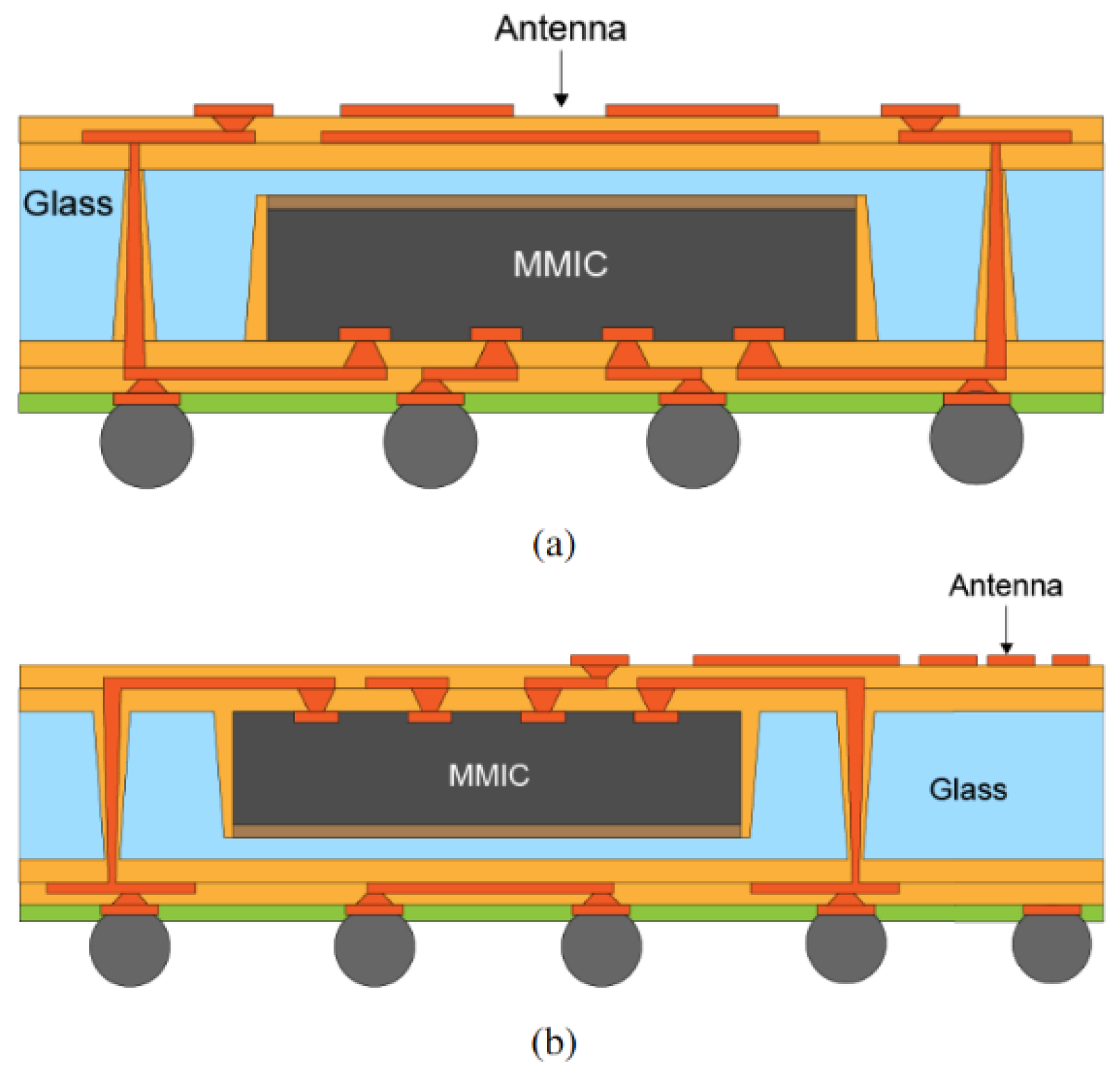
Figure 15c shows the embedded Glass Interposer Package after assembly and capillary underfill. Figure 16 shows example architectures with antenna integrated with MMIC using the GPE approach. This kind of integration scheme provides lower insertion and parasitic losses.

Figure 16.
Antenna in package (AiP) architecture schemes using Glass Panel Embedding (a) Die facing down and (b) Die facing up [61].
3.2. Optics Integration
The ability to microstructure glass substrates presents a key enabler for advanced optical integration, particularly in the context of co-packaged optics. Multiple waveguide fabrication techniques are possible, including ion-exchange diffusion [62], femtosecond laser-induced refractive index modification [63,64,65], and through-glass vias TGVs filled with optically transparent polymers, enabling both planar and vertical (3D) waveguide architectures. Furthermore, photonic integrated circuits (PICs) can be embedded within glass cavities to facilitate high-density co-integration with electronic ICs [66]. Grenier et al. demonstrated a scalable method for integrating high-density, low-loss fiber-to-chip connectivity in glass substrates using ultrafast Bessel beam laser processing. Ion-exchanged waveguides were formed in glass wafers and singulated with optical-quality end-facets, eliminating the need for polishing. Passive alignment was enabled via laser-ablated trenches for multi-fiber push-on (MPO) connectors, resulting in a lower 0.19 dB loss compared to active alignment [67].
Ion exchange is a well known process that has been used since 1972 for locally modifying the optical properties of glass [62]. This ability makes glass an ideal platform for co-packaged optics. Brusberg et al. have demonstrated ultra-low-loss ion-exchanged (IOX) waveguides in a newly engineered alkali glass composition with a propagation loss of 0.034 dB /cm and thermal stability suitable for five-year operation at 85 °C. To mitigate alkali ion migration into adjacent materials, a thin SiO2 barrier layer (<200 nm) was introduced, maintaining coupling losses below 0.5 dB to photonic ICs [68]. In another report, Brusberg et al. presented a co-packaged optics platform in a compact, low-cost substrate. Using ion-exchanged waveguides with <0.1 dB/cm loss, through-glass vias, and fine-line copper redistribution layers embedded in 50 μm-deep cavities, their design supported high-density optical and electrical interconnects. Low-loss (∼0.5 dB) coupling to silicon nitride PICs and edge fiber connectivity via a novel 4.4 mm-high connector were demonstrated. Passive alignment features resulted in connector losses as low as 0.85 dB. Figure 17a shows a schematic of glass platform with assembled PIC and Figure 17b shows an optical micrograph with waveguides located just below the glass surface [69,70,71].

Figure 17.
(a) Glass platform with assembled PIC for fiber-to-chip and chip-to-chip optical connectivity with RDL, TGVs, and IOX waveguides. (b) End-facet optical micrograph showing waveguides located just below the glass surface at pitch of 250 microns same as fiber pitch in a MPO fiber array connector [69].
Apart from waveguides, other optical components such as mirrors and lenses can also be integrated with glass substrates. Chou et al. demonstrated a 3D glass photonic interposer with integrated micro-mirrors and lenses with low-loss (<0.5 dB), low-cost, and alignment-tolerant single-mode fiber coupling. In another report, Vis et al. demonstrated a self-aligned 3D polymer waveguide with 45° total internal reflection micro-mirrors in ultra-thin glass interposers for chip-to-chip optical links. Using a novel inclined lithography process, <0.5 dB loss and 2.5 μm alignment tolerance were achieved across four-inch panels using scalable PCB-compatible fabrication [72,73].
3.3. mmWave Passives and Interconnects
Leveraging advanced glass processing technologies, mmWave interconnects and components have been developed to exhibit low loss, minimal dispersion, high power-handling capability, and excellent broadband performance. This section presents a brief review of recent advancements in glass-based packaging for mmWave applications [74].
3.3.1. Interconnects
The highly integrated packages with the SoP technology in the mmWave spectra place more demands on the number of metal layers in a packaging substrate for signal routing, power or current distribution, and ground planes. In-package signal routing includes transmission lines, through-package vias (TPVs), and microvias, which connect signal traces or planes in different layers.
To achieve optimal performance in mmWave packages, interconnects linking various devices and passive components must exhibit low signal loss [75]. The exceptional dimensional stability of glass substrates further supports fine-line patterning, ensuring impedance matching and minimal insertion loss.
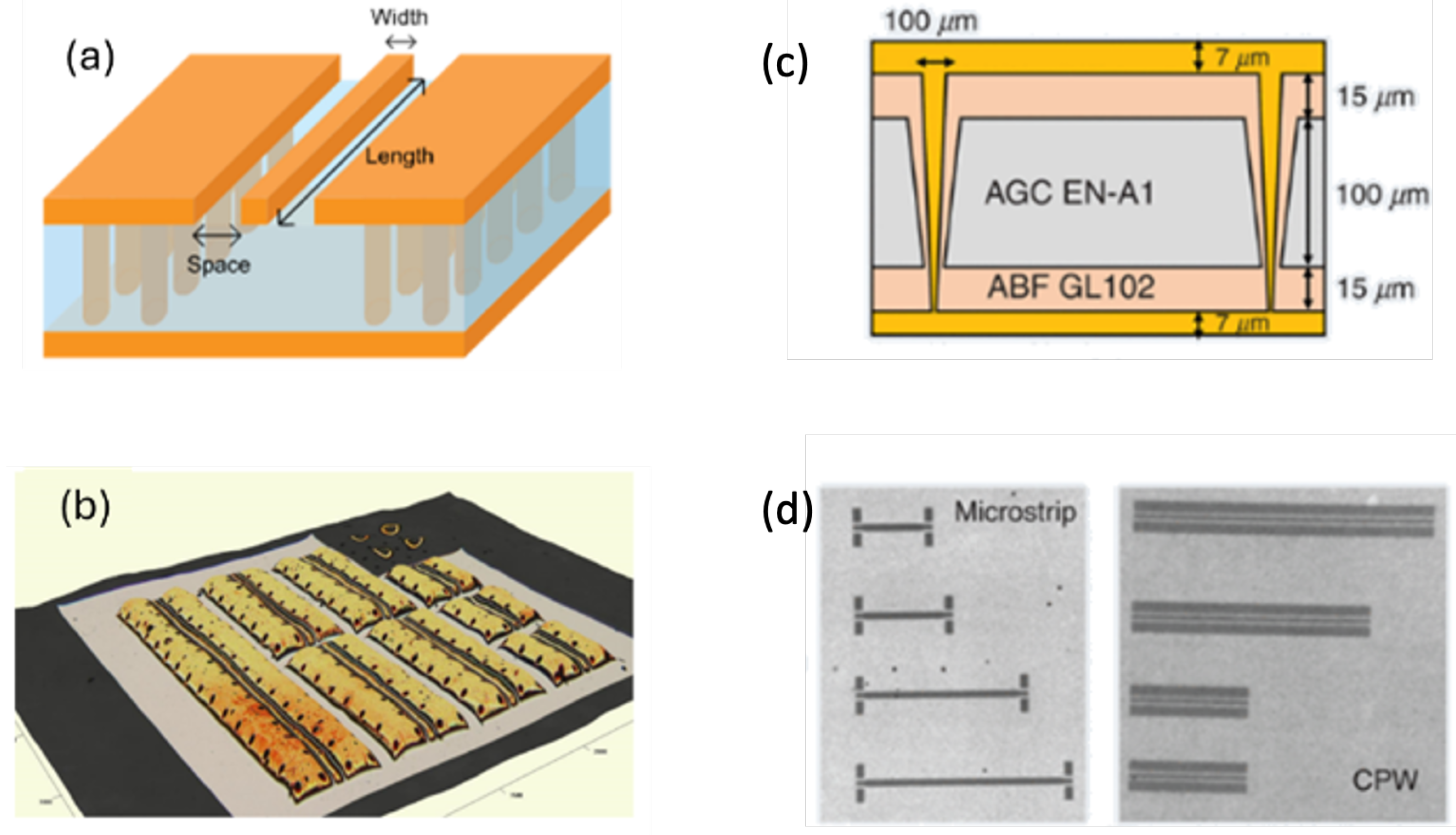
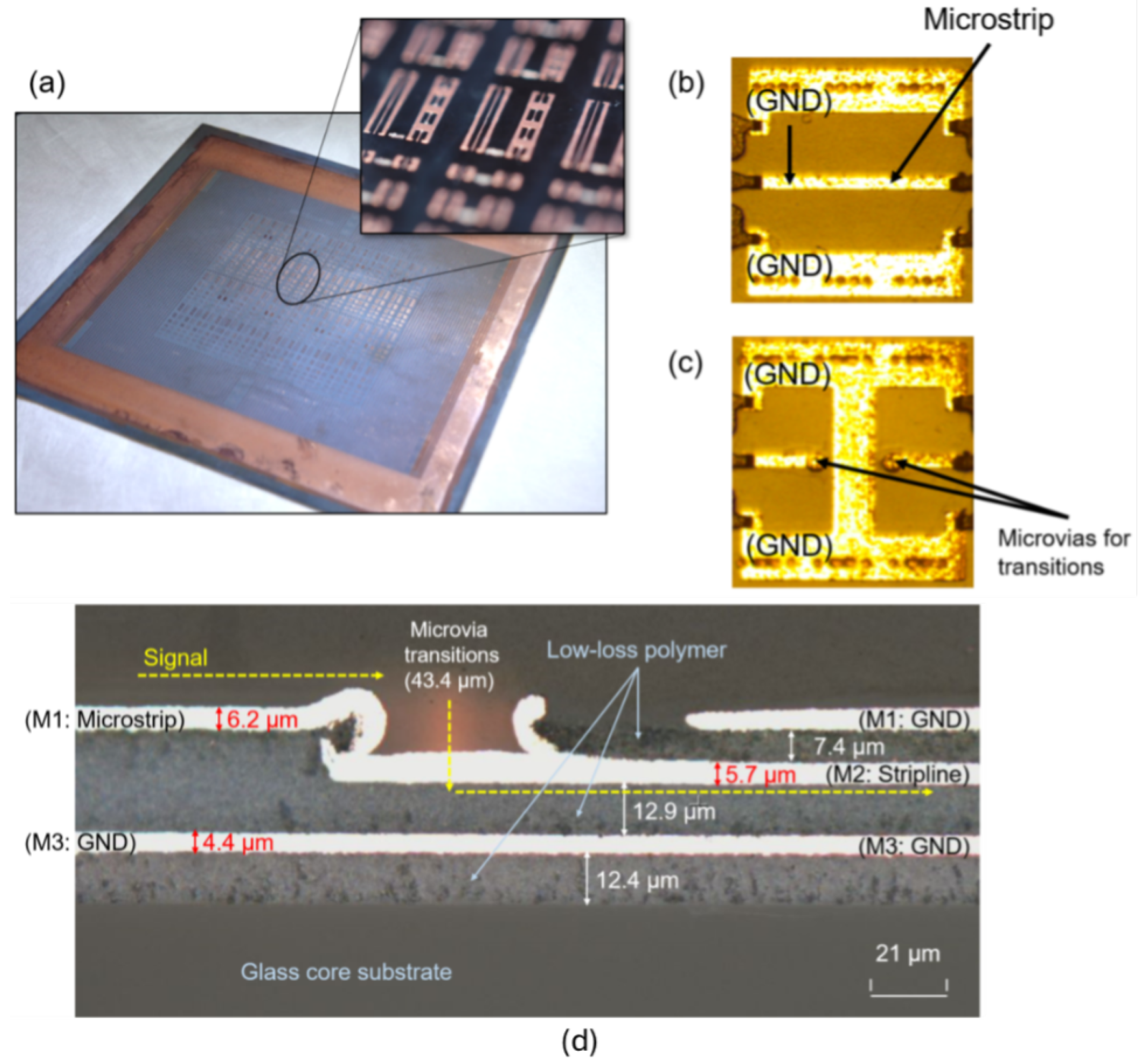
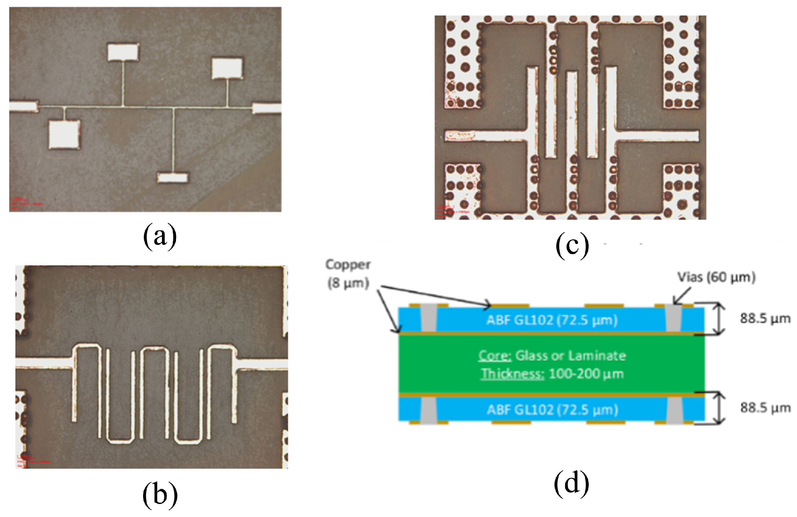
Various interconnects, like microstrip and coplanar waveguide (CPW) and conductor-backed CPW (CB-CPW), have been fabricated and characterized [76,77]. Figure 18 shows the microstrip line and CPW structures fabricated on glass for the 5G band and ABF/Glass/ABF stack-up in D-band. The extracted loss of microstrip lines shows 0.1–0.122 dB/mm at the 5G mmWave band (28–40 GHz) and 0.45 dB/mm at 140 GHz, while the CPWs show a 0.075–0.095 dB/mm loss at the 5G mmWave band and 0.25 dB/mm at 140 GHz. Daisy chain structures were fabricated to characterize the behavior of microvias in mmWave bands as shown in Figure 19 [77].

Figure 18.
CPW on glass. (a) Stack-up. (b) Fabricated CPWs with different lengths [78]. (c) Stack-up for D-band designs. (d) Fabricated microstrip lines and CPWs with different length [76].

Figure 19.
(a) Fabricated glass panel with low-loss interconnects, with the inset of a magnified image. (b) Line section. (c) Daisy chain. (d) Cross-section of the daisy chain [79].
Another family of vertical interconnects are capacitive and inductive interconnects. Via-less interconnects work on the principle of capacitive and inductive coupling to form an electrical interconnection. The size of the patch affects the parasitics in the interconnect and defines its frequency of operation. The proposed via-less interconnect in [80] works on the basis of capacitive coupling as shown in Figure 20. It has an insertion loss of less than 2 dB even at 170 GHz.

Figure 20.
(a) The proposed vertical via-less interconnect. (b) Material stackup for the demonstration of Interconnects. (c) Fabricated interconnects [80].
3.3.2. Substrate Integrated Waveguides (SIW)
As the frequency of operation scales up, the dimensions of the waveguides are minimized, which enables them to be integrated into the package easily. SIW is popular in the field of RF engineering due to its inherent shielding and high Q benefits. Figure 21a introduces the SIW on ABF/Glass/ABF stack-up and Figure 21b introduces an air-filled astra on glass [81,82]. The measured SIW presents 0.5–0.8 dB/mm across the entire D-band. The reported air-filled SIW presents a 0.13–0.2-dB/mm loss across D-band.
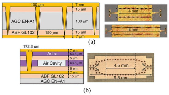
Figure 21.
SIW on a glass substrate. (a) SIW on an ABF/glass/ABF stack [81]. (b) Air-filled SIW on glass [82].
3.3.3. Filters
An RF filter belongs to one of the classifications of electronic filters and it is designed to pass desired frequencies while blocking the undesired ones. In the context of system integration, filters must have excellent performance, miniaturization, and process compatibility.
Highly miniaturized band-pass and low-pass filters are designed and fabricated on a glass substrate in the 5G NR frequency bands covering 28 GHz and 39 GHz communication bands [83]. The overall dimensions of the filters are lower than 0.5 × 0.5 . The insertion loss was minimized by using low dielectric loss materials to less than 2.6 dB midband for a fifth-order filter. A performance comparison of the filters is presented in [84]. Figure 22 shows the fabricated filters.

Figure 22.
Fabricated filters for 5G mm-wave bands. (a) Ninth-order LPF for 28 GHz band. (b) Fifth-order interdigital BPF. (c) Fifth-order hairpin filters. (d) Sackup of the test vehicle. [83].
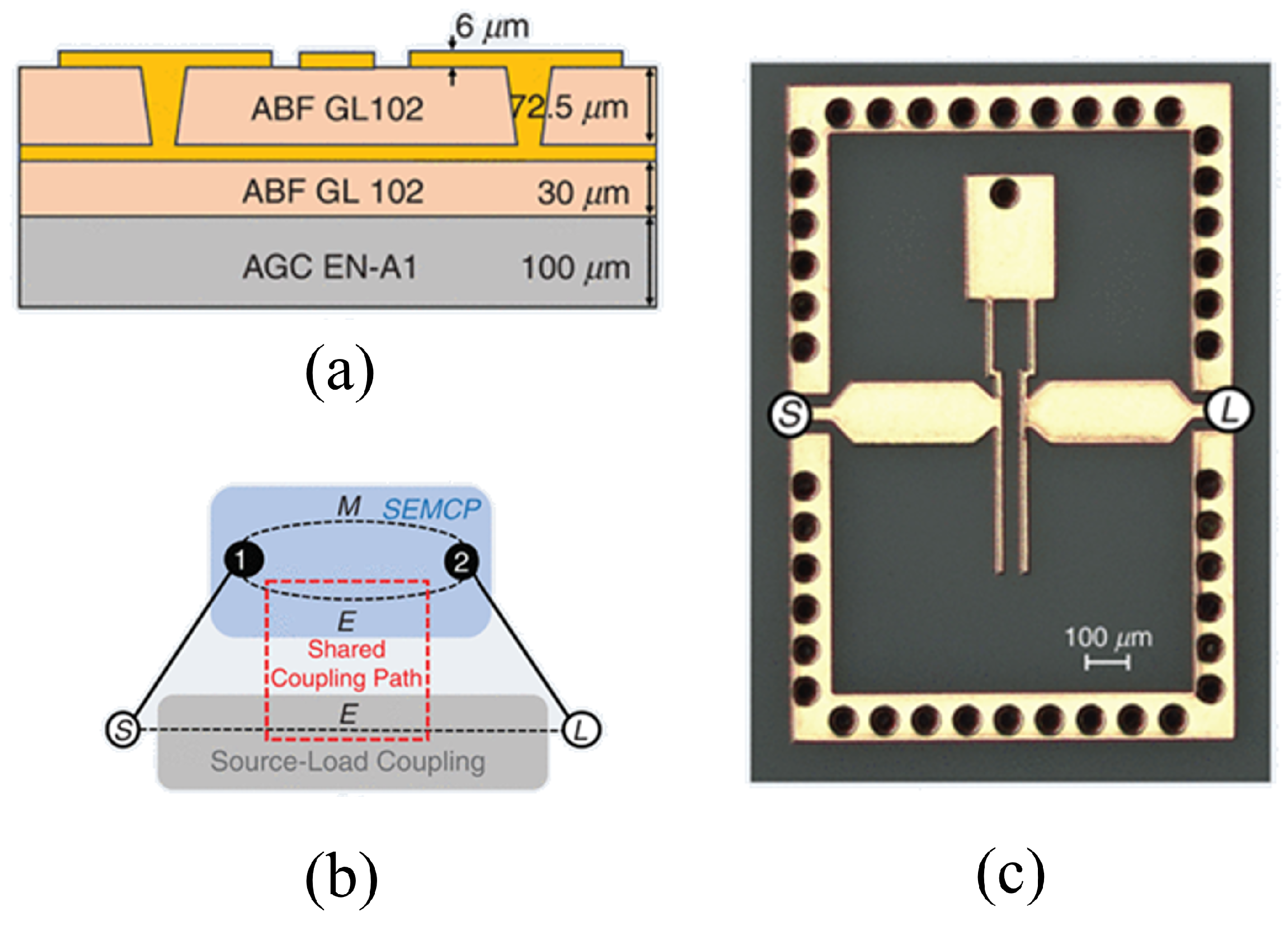
Furthermore, an advanced D-band filter centered at 140 GHz based on four out-of-band transmission zeros (TZs) and source-load direct coupling was designed and fabricated on glass [85]. Figure 23 presents the stack-up, topology, fabricated structure, and measured response. Centered at 140 GHz, the filter realizes a 3 dB bandwidth of 6.5% with a dimension of only 0.48 and a 1.19 dB in-band insertion loss. Bartlet et al demonstrated a structured-glass waveguide technology with a fourth-order Chebyshev bandpass filter at 88 GHz (2.3% FBW). The prototype achieved 1.43–1.97 dB insertion loss, >22 dB return loss, and only 0.117% center-frequency offset, validating its potential for advanced W-band systems [86].

Figure 23.
A multi-TZ bandpass filter. (a) Stack-up. (b) Filter topology. (c) Fabricated filter [85].
3.3.4. Antenna in Package (AiP)
AiP enables the design of smaller and more compact devices by efficiently utilizing the available space with enhanced performance and reliability. Systems with 5G connectivity impose several challenges associated with high frequency designs, materials and processes, interconnect losses, and the process control necessary for precision impedance match. Distributed components with careful control of parasitics and propagation losses are needed. Miniaturized antennas with high bandwidth and gain are also needed. Various antenna implementations on glass have been demonstrated. A comprehensive review of antennas for D bands were compiled by De et al. [87].
Broadside antennas radiate energy perpendicular to the plane of the antenna. They offer easier design rules with high directivity. Figure 24b shows a 4 × 4 Patch antenna array having a bandwidth between 137 and 144-GHz bandwidth and 16.2-dBi boresight gain; this was discussed in [88] and the advantages and process of embedding dies in the glass substrate were described in [41] by using a 1 × 8 series fed antenna centered at 140 GHz.
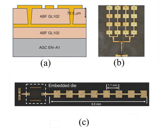
Figure 24.
A 4 × 4 antenna array. (a) Stack-up. (b) Fabricated sample [88]. (c) Fabricated antenna with embedded chip [41].
End-fire antennas launch energy along the direction of the antenna directors. They offer significant advantages including high gain and directivity, wide impedance-matched bandwidth, low complexity, and integration.
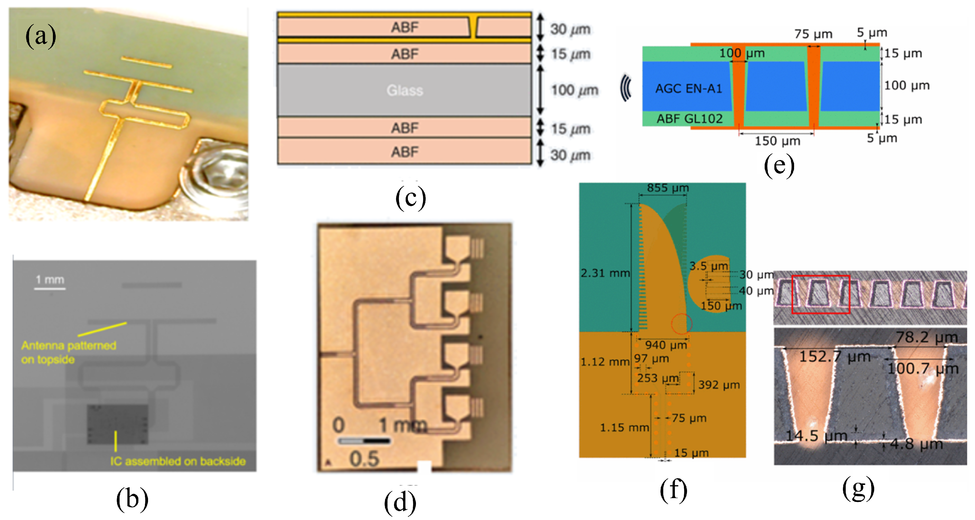
A compact dipole Yagi-Uda with assembled antenna operating in the 5G NR band fabricated on a glass substrate was described by Watanabe et al. [89] as shown in Figure 25a,b. A printed quasi-Yagi antenna with a monopole radiator having almost complete bandwidth from 110–170 GHz was discussed by Erdogan et al. [90] is depicted in Figure 25d. It simplifies the design rules of the antenna from requiring a balun as in the prior case while offering all the benefits. A Vivaldi-inspired SIW-based antenna offering higher gain was discussed in [91] is as presented in Figure 25f. The antenna also offers a wide bandwidth covering the whole of the D band. This case makes use of the substrate core in realizing the antenna rather than using the glass just for the mechanical benefits as in the prior examples where the antenna is built in the buildup layers.

Figure 25.
(a) Diced Yagi-Uda antenna element assembled with a 2.92-mm end launch connector. (b) X-ray inspection of the Yagi-Uda antenna with an assembled LNA [89]. (c) Stack-up of the printed quasi-Yagi antenna. (d) Fabricated 1 × 4 linear array [90]. (e) Stack-up of the Vivaldi inspired antenna. (f) Designed antenna element and cross-section of the fabricated antenna. (g) Cross-section of the TGVs [91].
3.4. Thermal Management
Glass, with a thermal conductivity of 0.5–1.38 W/m·K, is a good thermal insulator. While this low conductivity poses challenges for closely integrating heat-dissipating components like HBMs and GPUs, it also enables a unique advantage—allowing glass packages to thermally isolate individual chips. Embedding chips in separate cavities makes glass a thermal barrier between two chips providing thermal isolation and eliminating thermal crosstalk. This capability is becoming very useful as the system power keeps increasing, and heterogeneous chiplet integration becomes the norm. Different architectures for thermal management have been explored in the literature.
Nedumthakady et al. demonstrated a Glass Panel Embedded (GPE) package with integrated copper heat spreaders directly bonded to RF dies, achieving near-zero thermal interface resistance, shown in Figure 26a,b. The design mitigated CTE mismatch via stress buffers and used ultra-low-loss dielectrics, enabling efficient thermal management and GHz-band performance for 30–100 W power amplifiers [92]. Different kinds of architectures have been demonstrated for GPE packages and an example is shown in Figure 27. Wong et al. evaluated an open backside Glass Panel Embedded package with an integrated heat spreader that demonstrated excellent thermal performance, sustaining 10.3 W/cm2 with passive air cooling and up to 70.3 W/cm2 with advanced liquid cooling while maintaining a 100 °C device temperature. Thermal modeling showed more uniform temperature gradients and reduced hot spots due to the direct heat spreader interface. Additionally, glass’s low thermal conductivity enabled effective thermal isolation, lowering substrate temperatures by about 20% compared to silicon [93].

Figure 26.
(a) Direct bonded copper heat spreaders in high-power GPE packages. (b) Magnified image of conformal copper heat spreader [92].

Figure 27.
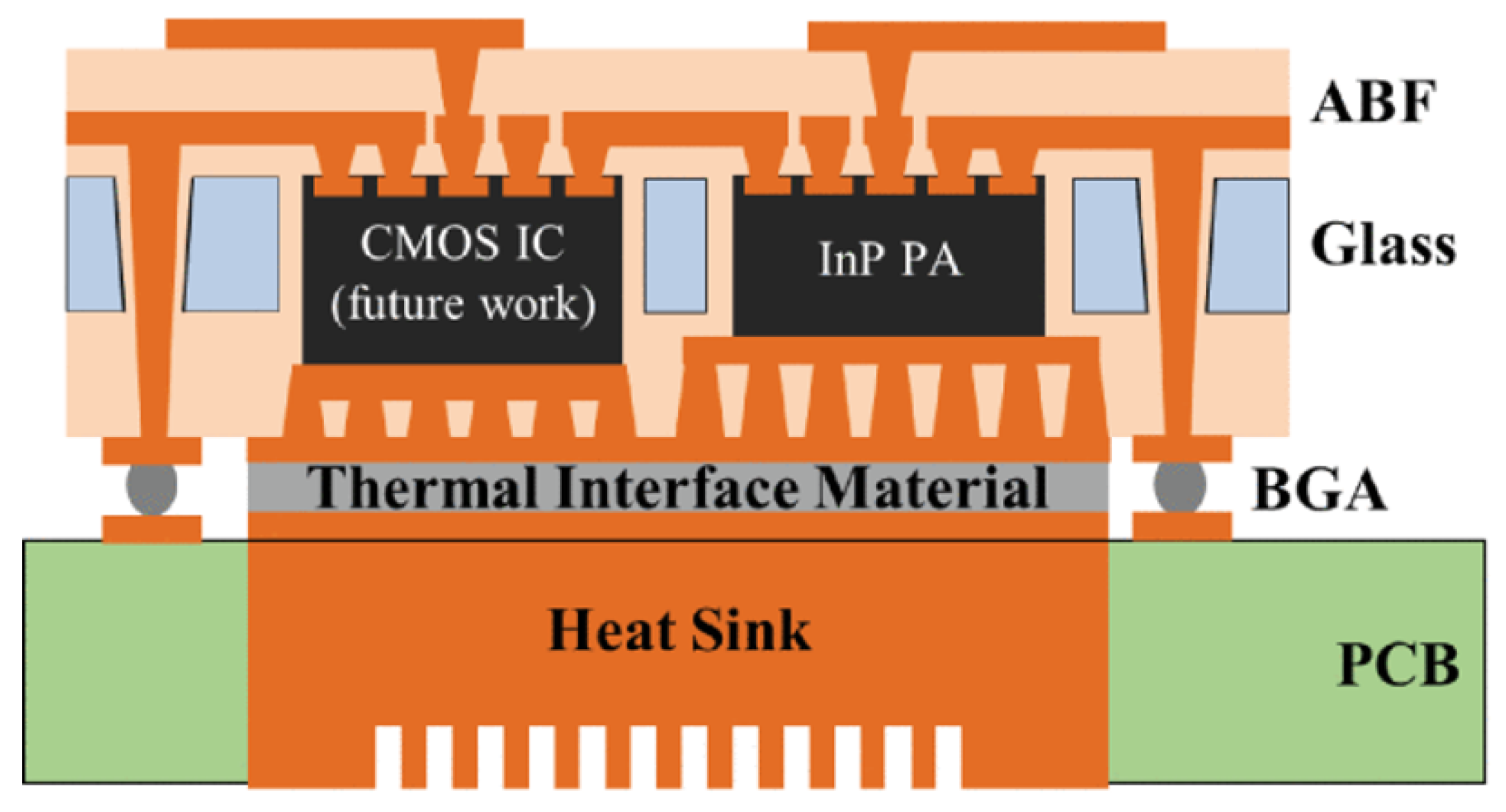
Antenna-Integrated and PA-embedded architecture with thermal vias for heat removal [94].
Thermal vias can also be utilized to provide pathways for heat removal from the bottom of the substrate. Cho et al. evaluated the thermal performance of glass interposers with copper through-package vias (TPVs). Experimental and simulation results showed that TGVs can significantly boost out-of-plane thermal conductivity by up to 20 times and reduce junction temperatures [95].
4. Manufacturing Challenges
Manufacturing glass substrates at high volume presents several challenges, primarily stemming from the material’s brittleness and the difficulty of achieving a high TGV yield. Together, these factors remain the primary barriers to widespread adoption and production scalability.
4.1. Glass Cracking
Cracks and scratches are often introduced during the handling of the incoming glass panel, especially at the edges. A tiny scratch or crack can propagate in subsequent fabrication steps. It is harder to prevent cracks in the case of rectangular panels with edges and corners compared to circular wafers. The corners of large glass panels are typically rounded to reduce the instances of crack formation and propagation from the corners of the panels. Polymer dielectric lamination on glass also helps to prevent cracks to a certain extent.
After TGV copper filling, subsequent processing steps can induce stress within the glass core. This can potentially initiate new cracks or propagate existing ones, leading to sudden yield loss. This is exacerbated during the CMP or lamination steps when pressure is applied to the glass. Key measures currently used include automated robotic substrate handling, strict incoming quality control, careful CTE matching between glass and package components, and statistical defect monitoring.
Crack formation during the singulation or dicing of glass substrates is a critical manufacturing problem. Three key crack types affect glass-core substrates: cohesive cracks, interfacial delamination, and sequential failures from dicing damage [96,97]. While delamination is manageable, cohesive cracking that is driven by interface stress and micro-defects is a major concern unique to glass. These cracks often initiate during or after dicing and compromise substrate integrity.
McCann et al. used 2D finite element analysis to evaluate how RDL thickness, edge pull-back, and defect size affect crack propagation in glass-core substrates [96,97]. They found that the energy release rate (ERR) increases with defect size, while reducing the dielectric/metal thickness lowers the ERR. Thicker glass marginally reduces the ERR, though results depend on defect location. Due to variability in defect positions, maximum principal stress is also a critical fracture indicator.
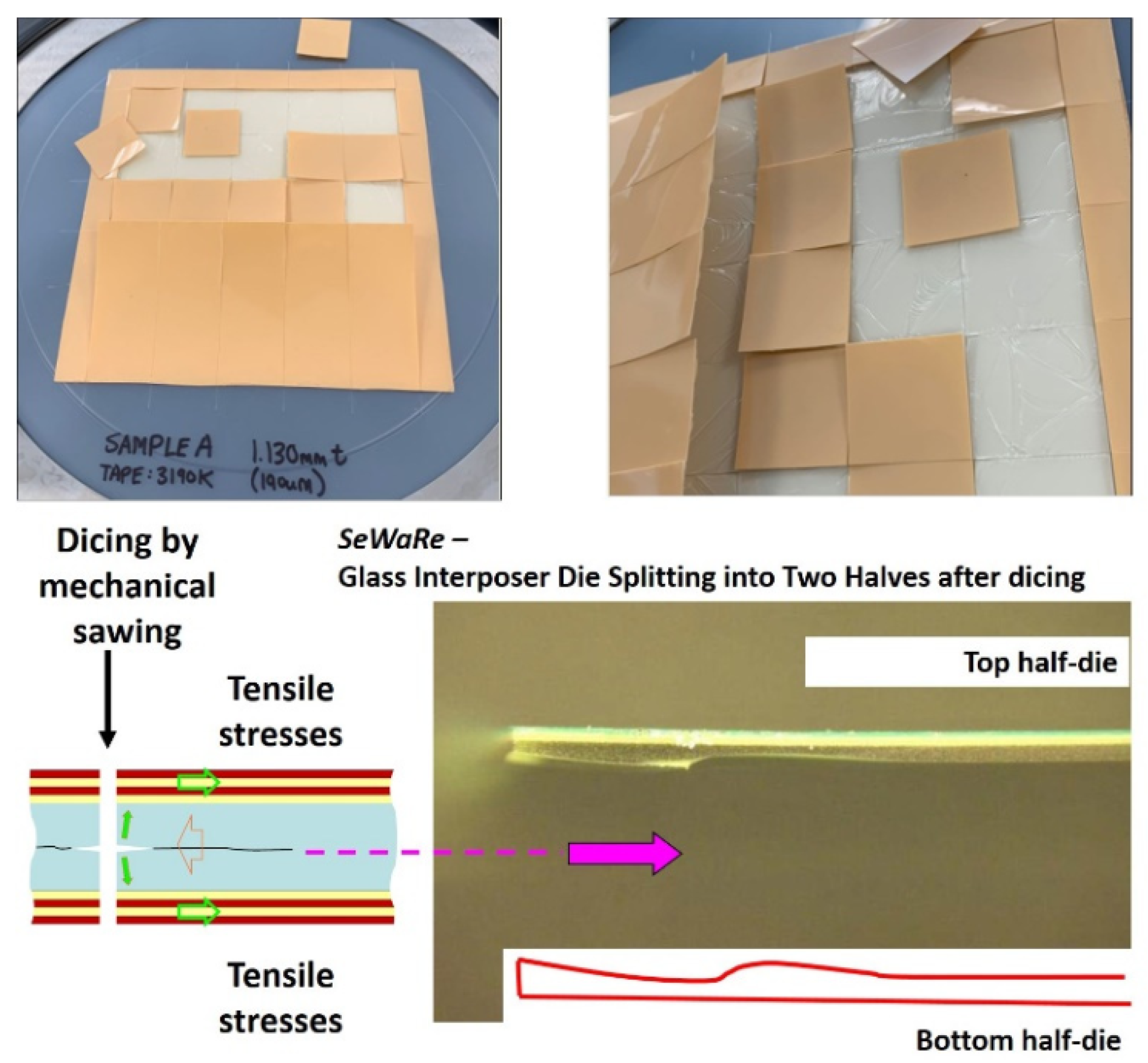
Laminated dielectric layers induce tensile stresses on glass. The dicing process can cause cracks to initiate and propagate within the glass core. This phenomenon is termed SeWaRe, derived from a Japanese phrase meaning “splitting of the back” [98]. Wei et al. compared four dicing techniques on borosilicate glass and found that die strength was not determined by chipping or roughness, but by internal stress concentrators influenced by dicing parameters. SeWaRe failures occurred when dielectric layers extended to the die edge, creating high energy release rates during dicing. A pull-back geometry was introduced where the die edges were partially or completely free of the build-up layers. An optimized pull-back geometry eliminated cracks and was determined to be the best-known approach for maximizing substrate reliability. Figure 28 shows pictures and schematics to explain these failures.

Figure 28.
Illustration of SeWaRe dicing failures [98].
4.2. TGV Process Control and Yield
The formation and metallization of TGVs are critical challenges that have slowed the adoption of glass substrates [99]. The first part of the problem is the yield and repeatability of TGVs. Precise control of via diameters (top, bottom, and waist) is essential for reliable physical vapor deposition(PVD) seed layer coverage. The hourglass or re-entrant via shapes complicate deposition, often requiring double-sided PVD. CD variations can arise from both laser and local variations in glass composition or chemical processes. These need to be closely monitored using high-speed automated optical inspection (AOI). Every TGV must be open and free of defects. Defect detection uses AOI in combination with CAD verification to identify missing or defective vias among millions. Another way to tackle this issue is by having redundancy in the TGV layout.
As an example, in the case of photosensitive glass processing, the exposure step needs to be precisely controlled. This, in turn, makes it necessary for the precise measurement and control of radiation intensity, and exposure time. Any variation in these would result in a variation in the size of vias. Any variation in the concentration of hydrofluoric acid also contributes to variation in via dimensions. If the variation of dimensions exceeds the tolerance, large batches of glass panels will need to be scrapped. Another issue with photo-patterning and plasma etching of vias is that some of the vias might not etch all the way to the bottom. There are some instances where vias might not get etched at all, resulting in missing vias.
The second part of the problem is the metallization of TGVs. There are several challenges associated with electroplating large glass panels. It is harder to maintain uniform current density across larger panels. The plating rate is higher at the perimeter compared to the center. If the design consists of several via dimensions, it is harder to optimize the plating process parameters in a way that all the vias are plated uniformly.
As the industry diverges between full copper fill and partial metal/dielectric fill strategies, new defects such as voids, divots, and surface pimples emerge. The filled vias are beneficial in reducing electrical losses. However, the higher volume of plated copper results in higher residual stresses. These kinds of vias are also more likely to have voids in the plated copper. Advanced tools like acoustic imaging and interferometric sensors are used to characterize and inspect these features. Because of the high via density and shrinking geometries (<100 μm), real-time inspection and AI-driven failure classification are essential for identifying early-stage killer defects and improving pilot line reliability. There are multiple companies marketing their AOI products toward glass substrate manufacturing [100,101,102,103]. Identification and mitigation of defects early in the process flow can reduce further yield losses.
5. Current State of Commercialization
Over the past two years, there has been a growing number of announcements from major semiconductor and packaging companies about their efforts to develop and commercialize glass-core substrates. Companies are investing in pilot lines, demonstrating prototypes, and building new R&D and production facilities in the U.S, Japan, and Europe. The explosion of AI-driven applications has led to the demand for higher computing power and the adoption of new technologies. Several companies plan to bring products to market in the next few years [104,105,106,107,108,109], with some, such as Absolics, already initiating test production in preparation for commercial deployment by 2025 [105,106]. Figure 29 shows pictures of glass substrates manufactured by Absolics and Intel on 610 × 615 mm panels.

Figure 29.
Pictures of glass substrate manufactured by (a) Absolics [110] and (b) Intel [108].
Among these efforts, a few companies have disclosed notable differences in their approaches. Absolics, for example, is offering glass substrate with embedded MLCCs as their principal product. FICT has demonstrated its G-ALCS (Glass All Layer Z-connection Structure) technology, which connects all layers of a bonded glass stack through a resin interface to create a vertically integrated structure [111]. Intel has presented samples with three build-up layers on glass, highlighting improved reliability, power delivery, and mechanical stability over organic substrates [108]. Qorvo, through the SHIP-RF program, is developing panel-sized glass-core substrates with embedded passives and fine-pitch RDLs, specifically targeting RF and mixed-signal microsystems [112]. DNP has published several papers with high-density RDL on glass [48]. 3DGS has recently raised funding and announced plans to enter glass substrate manufacturing [113].
Other companies including Ibiden, SEMCO, Shinko, Toppan, Unimicron, LG Innotek, Samsung, and AT&S have announced R&D initiatives in glass substrate technologies but have not publicly disclosed differentiated approaches or technical breakthroughs. Their activities remain within the broader context of material exploration, process development, and roadmap alignment with future packaging needs [114,115].
6. Future Needs
As microelectronic systems grow in complexity, the future of computing will be increasingly defined by how well we can integrate and interconnect diverse chiplets more closely and efficiently. Traditional packaging technologies have failed to keep pace with silicon scaling, creating a widening gap in performance and efficiency. To meet the demands of AI, high-performance computing, and data-intensive applications, packaging must evolve beyond legacy technologies. This shift demands the following improvements.
6.1. System on Panel
The next generation of advanced packaging will require scaling down interconnect features to near-monolithic levels and scaling out to enable dense, heterogeneous integration across large packages. The ultimate ambition for glass-substrate packaging is to support up to a million I/Os per package [116] or tens of millions of I/Os per panel, enabling the full realization of “system-on-panel” architectures that potentially encompass an entire data center rack. This builds on TSMC’s System-on-Wafer (SoW), which facilitates fan-out packaging at wafer scale and integrates massive interconnect density. Glass substrates can extend this concept to even larger panels, supporting denser interconnect networks and chiplet integration.
6.2. Low-Stress Materials and Processes
Glass cracking during processing and after singulation are major limiters to enabling larger panels and package sizes. The fundamental reason for this lies in the mismatch between the nature of polymer dielectrics and inorganic glass. For continuing system scaling using glass substrates, it is critical to develop and adopt low-stress materials and processes. Adopting back-end-like processing approaches along with a lower thermal budget of the entire process flow is necessary.
6.3. Sub-Micron Tolerances and Standardization of Large Panels
Achieving <1 μm line/space tolerances on the scale of 500 mm × 500 mm glass panels requires back-end-level precision. Glass already offers superior flatness and stiffness. However, conventional polymer dielectrics and semi-additive processes do not provide the same level of precision and degrade tolerances with the buildup of layers. Planarization at a panel scale will be a critical technique in the future for improving tolerances. The industry-wide standardization of panel sizes and materials is essential to align efforts and focus collective resources on addressing key manufacturing challenges.
6.4. Better Handling, Inspection, and Cleanliness
As packaging and back-end become intertwined, it is clear that large panel-scale manufacturing needs to be similar to back-end manufacturing. Traditional manual or semi-manual substrate processing is detrimental because of the brittle nature of glass. Automated handling and optical inspection systems are already being adopted. Cleanliness levels also need improvement. Traditional packaging and substrate manufacturing are carried out in cleanrooms of class 1000 (ISO 6) to class 10,000 (ISO 7), while advanced packaging techniques such as hybrid bonding require Class 100 (ISO 5) to Class 1000 (ISO 6). Contamination control in wet substrate processing methods, such as electroplating, also requires significant improvement. More broadly, packaging processes across the board must become cleaner to meet advanced manufacturing demands.
Funding
This research was funded by the industry consortium at the 3D Systems Packaging Research Center, Georgia Institute of Technology, Atlanta, GA, USA.
Conflicts of Interest
Pratik Nimbalkar is employed by Plaid Semiconductors Inc.
Abbreviations
The following abbreviations are used in this manuscript:
| GPU | Graphics Processing Unit |
| HBM | High Bandwidth Memory |
| RDL | Redistribution Layer |
| TSMC | Taiwan Semiconductor Manufacturing Company |
| CoWoS | Chip-on-Wafer-on-Substrate |
| EMIB | Embedded Multi-die Interconnect Bridge |
| BEOL | Back-End-Of-Line |
| UCIe | Universal Chiplet Interconnect Express |
| ASIC | Application-Specific Integrated Circuit |
| LSI | Local Silicon Interconnect |
| CTE | Coefficient of Thermal Expansion |
| EMC | Epoxy Mold Compound |
| TGV | Through Glass Via |
| ICP RIE | Inductively Coupled Plasma Reactive Ion Etching |
| DC | Direct Current |
| LIDE | Laser Induced Deep Etching |
| RF | Radio Frequency |
| MEMS | Micro-Electro-Mechanical Systems |
| SEM | Scanning Electron Microscope |
| WLFO | Wafer-Level Fan-Out |
| SAP | Semi-Additive Process |
| BGA | Ball Grid Array |
| PCB | Printed Circuit Board |
| C4 | Controlled Collapse Chip Connection |
References
- Duan, G.; Zhang, Y.; Gunawan, A.; Fang, Y.; Mousavi, J.; Apte, A.A.; Ahmed, N.; Sharma, S.; Alur, S.; Chandolu, A.; et al. EMIB-TSV Advanced Packaging Technology—EMIB’s Next Evolution. In Proceedings of the 2025 IEEE 75th Electronic Components and Technology Conference (ECTC), Dallas, TX, USA, 27–30 May 2025. [Google Scholar]
- Mahajan, R.; Manepalli, R.; Aygün, K.; Radhakrishnan, K.; Sharan, S. Scaling EMIB—A Comprehensive Architecture Portfolio for Localized Interconnects. IEEE Trans. Electron Devices 2025, 72, 3911–3914. [Google Scholar] [CrossRef]
- Shih, P.C.; Su, A.J.; Tam, K.H.; Huang, T.C.; Chuang, K.; Yeh, J. SoW-X: A Novel System-on-Wafer Technology for Next Generation AI Server Application. In Proceedings of the 2025 IEEE 75th Electronic Components and Technology Conference (ECTC), Dallas, TX, USA, 27–30 May 2025. [Google Scholar]
- Kim, Y. Electrical Performance Analysis of High-Speed Interconnection and Power Delivery Network (PDN) in Low-Loss Glass Substrate-Based Interposers. Micromachines 2023, 14, 1880. [Google Scholar] [CrossRef]
- Sawyer, B.M.D.; Suzuki, Y.; Furuya, R.; Nair, C.; Huang, T.C.; Smet, V.; Panayappan, K.; Sundaram, V.; Tummala, R. Design and Demonstration of a 2.5-D Glass Interposer BGA Package for High Bandwidth and Low Cost. IEEE Trans. Compon. Packag. Manuf. Technol. 2017, 7, 552–562. [Google Scholar] [CrossRef]
- Vanna-Iampikul, P.; Woo, S.; Erdogan, S.; Zhu, L.; Kathaperumal, M.; Agarwal, R.; Gupta, R.; Rinebold, K.; Swaminathan, M.; Kyu Lim, S. Glass Interposer Integration of Logic and Memory Chiplets: PPA and Power/Signal Integrity Benefits. IEEE Trans. -Comput.-Aided Des. Integr. Circuits Syst. 2025, 44, 1954–1967. [Google Scholar] [CrossRef]
- Du, K.; Shi, P. Subsurface precision machining of glass substrates by innovative lasers. Glass Sci. Technol. 2003, 76, 90–95. [Google Scholar]
- Bernd, K.; Horst, E.; Udo, L.; Thomas, K. Drilling of glass by excimer laser mask projection technique. J. Laser Appl. 2000, 12, 189–193. [Google Scholar] [CrossRef]
- Sukumaran, V.; Kumar, G.; Ramachandran, K.; Suzuki, Y.; Demir, K.; Sato, Y.; Seki, T.; Sundaram, V.; Tummala, R.R. Design, Fabrication, and Characterization of Ultrathin 3-D Glass Interposers with Through-Package-Vias at Same Pitch as TSVs in Silicon. IEEE Trans. Compon. Packag. Manuf. Technol. 2014, 4, 786–795. [Google Scholar] [CrossRef]
- Liu, J.; Xia, C.; Ming, X.; Yin, C. Optimization of Laser-induced Deep Etching for TGV Fabrication in Fused Silica. In Proceedings of the 2023 24th International Conference on Electronic Packaging Technology (ICEPT), Shihezi City, China, 8–11 August 2023; pp. 1–6. [Google Scholar] [CrossRef]
- Sandström, N.; Brandt, L.; Sandoz, P.A.; Zambarda, C.; Guldevall, K.; Schulz-Ruhtenberg, M.; Rösener, B.; Krüger, R.A.; Önfelt, B. Live single cell imaging assays in glass microwells produced by laser-induced deep etching. Lab Chip 2022, 22, 2107–2121. [Google Scholar] [CrossRef] [PubMed]
- Santos, R.; Delrue, J.P.; Ambrosius, N.; Ostholt, R.; Schmidt, S. Processing Glass Substrate for Advanced Packaging using Laser Induced Deep Etching. In Proceedings of the 2020 IEEE 70th Electronic Components and Technology Conference (ECTC), Orlando, FL, USA, 3–30 June 2020; pp. 1922–1927. [Google Scholar] [CrossRef]
- Yang, Y.; Chien, J.; Lyu, S.; Wei, T. Development of Straight, Small-Diameter, High-Aspect Ratio Copper-Filled Through-Glass Vias (TGV) for High-Density 3D Interconnections. In Proceedings of the 2025 IEEE 75th Electronic Components and Technology Conference (ECTC), Dallas, TX, USA, 27–30 May 2025; pp. 1036–1042. [Google Scholar] [CrossRef]
- Kolari, K. Deep plasma etching of glass with a silicon shadow mask. Sens. Actuators A 2008, 41, 677–684. [Google Scholar] [CrossRef]
- Brokmann, U.; Weigel, C.; Altendorf, L.M.; Strehle, S.; Rädlein, E. Wet Chemical and Plasma Etching of Photosensitive Glass. Solids 2023, 4, 213–234. [Google Scholar] [CrossRef]
- Huang, T.; Sundaram, V.; Raj, P.M.; Sharma, H.; Tummala, R. Adhesion and reliability of direct Cu metallization of through-package vias in glass interposers. In Proceedings of the 2014 IEEE 64th Electronic Components and Technology Conference (ECTC), Orlando, FL, USA, 27–30 May 2014; pp. 2266–2270. [Google Scholar] [CrossRef]
- Pandey, H.; Pawar, K.; Dixit, P. Localized surface roughening to improve adhesion of electroless seed layer in through-glass vias. Mater. Sci. Semicond. Process. 2024, 183, 108757. [Google Scholar] [CrossRef]
- Hunegnaw, S.; Liu, Z.; Fu, H.; Wang, J.; Merschky, M.; Mukai, K.; Magaya, T. VitroCoat GI - Ultra-thin adhesive layer for metallization of glass interposer. In Proceedings of the 2015 10th International Microsystems, Packaging, Assembly and Circuits Technology Conference (IMPACT), Taipei, Taiwan, 21–23 October 2015; pp. 149–152. [Google Scholar] [CrossRef]
- Liu, Z.; Hunegnaw, S.; Fu, H.; Wang, J.; Magaya, T.; Merschky, M.; Bernhard, T.; Shorey, A.; Yun, H. A metal oxide adhesion layer prepared with water based coating solution for wet Cu metallization of glass interposer. In International Symposium on Microelectronics; International Microelectronics Assembly and Packaging Society: Pittsburgh, PA, USA, 2015; Volume 2015, pp. 000365–000369. [Google Scholar]
- Xu, L.; Liu, G.L.; Zhang, H.W.; Wang, Y.; Feng, Z.S. Nano-silver Doped Zinc Oxides Adhesion Layer for Wet Copper Metallization of Glass Substrates. J. Electrochem. Soc. 2025, 172, 012507. [Google Scholar] [CrossRef]
- Chang, Y.H.; Lin, Y.M.; Lee, C.Y.; Hsu, P.C.; Chen, C.M.; Ho, C.E. Through glass via (TGV) copper metallization and its microstructure modification. J. Mater. Res. Technol. 2024, 31, 1008–1016. [Google Scholar] [CrossRef]
- Jarrett, S.; McWethy, K.; Flemming, J. Implementing Photosensitive Glass as a Solution in Thermal Management Applications. In Proceedings of the 2020 19th IEEE Intersociety Conference on Thermal and Thermomechanical Phenomena in Electronic Systems (ITherm), Orlando, FL, USA, 21–23 July 2020; pp. 647–653. [Google Scholar] [CrossRef]
- Kanungo, M.; Vaddi, R.; Okoro, C.; Pollard, S.; Mazumder, P. Metallization of Helium-Hermetic and Thermo-Mechanically Reliable Through Glass Vias (TGV) by Conformal Pinched Via (CPV) Approach. In Proceedings of the 2025 IEEE 75th Electronic Components and Technology Conference (ECTC), Dallas, TX, USA, 27 May 2025; pp. 1043–1046. [Google Scholar] [CrossRef]
- Through Glass Via (TGV). Available online: https://www.agc.com/en/products/electoric/detail/tgv.html (accessed on 2 July 2025).
- Shorey, A. Glass Package and Through Glass Via (TGV) for MEMS. In Proceedings of the IMAPS 19th Conference on DEVICE PACKAGING, Fountain Hills, AZ, USA, 13–16 March 2023; pp. 995–1018. [Google Scholar] [CrossRef]
- Through-Glass Vias. Available online: https://www.3dgsinc.com/through-glass-vias (accessed on 2 July 2025).
- LPKF Vitrion TGV Solutions. Available online: https://vitrion.lpkf.com/en/company (accessed on 2 July 2025).
- Plan Optik Packaging Wafers. Available online: https://planoptik.com/products/packaging-wafers/ (accessed on 2 July 2025).
- LPKF Vitrion. RF and mmWave Applications—Glass Substrates for Advanced Packaging. 2025. Available online: https://vitrion.lpkf.com/en/applications-products/radio-frequencies (accessed on 2 July 2025).
- NSC Anaake Glass Solutions. Available online: https://nsc-net.co.jp/en/anaake/ (accessed on 2 July 2025).
- DNP Through Glass Via News. Available online: https://www.global.dnp/news/detail/20169052_4126.html (accessed on 2 July 2025).
- Tecnisco TGV Technology. Available online: https://www.tecnisco.com/en/en_product/en_glass/en_tgv.html (accessed on 2 July 2025).
- High-Quality Borosilicate Glass TGV. Available online: https://www.galliumnitridewafer.com/sale-44812469-tgv-through-glass-via-technology-high-quality-borosilicate-glass-quartz.html (accessed on 2 July 2025).
- SkySemi TGV Services. Available online: https://www.sky-semi.com/tgvjs (accessed on 2 July 2025).
- Lante Semiconductor Applications. Available online: https://www.lante.com.cn/en/product/semiconductor-applications-103.html (accessed on 2 July 2025).
- Spierings, G. Wet chemical etching of silicate glasses in hydrofluoric acid based solutions. J. Mater. Sci. 1993, 28, 6261–6273. [Google Scholar] [CrossRef]
- Iliescu, C.; Chen, B.; Miao, J. On the wet etching of Pyrex glass. Sens. Actuators Phys. 2008, 143, 154–161. [Google Scholar] [CrossRef]
- Park, J.; Lee, N.E.; Lee, J.; Park, J.; Park, H. Deep dry etching of borosilicate glass using SF6 and SF6/Ar inductively coupled plasmas. Microelectron. Eng. 2005, 82, 119–128. [Google Scholar] [CrossRef]
- Iliescu, C.; Tan, K.L.; Tay, F.E.; Miao, J. Deep wet and dry etching of Pyrex glass: A review. In Proceedings of the ICMAT (Symposium F), Singapore, 8–10 May 2005; pp. 75–78. [Google Scholar]
- Moore, A.F.; Frantz, J.A.; Busse, L.E.; Sanghera, J.S. A Review of Reactive Ion Etching of Glass Materials. 2021. Available online: https://apps.dtic.mil/sti/citations/AD1150342 (accessed on 2 July 2025).
- Jia, X.; Li, X.; Erdogan, S.; Moon, K.S.; Kim, J.W.; Huang, K.Q.; Jordan, M.B.; Swaminathan, M. Antenna with embedded die in glass interposer for 6G wireless applications. IEEE Trans. Compon. Packag. Manuf. Technol. 2023, 13, 219–229. [Google Scholar] [CrossRef]
- Cheng, H.C.; Chung, C.H.; Chen, W.H. Die Shift Assessment of Reconstituted Wafer for Fan-Out Wafer-Level Packaging. IEEE Trans. Device Mater. Reliab. 2020, 20, 136–145. [Google Scholar] [CrossRef]
- Ravichandran, S.; Yamada, S.; Park, G.; Chen, H.W.; Shi, T.; Buch, C.; Liu, F.; Smet, V.; Sundaram, V.; Tummala, R. 2.5 D glass panel embedded (GPE) packages with better I/O density, performance, cost and reliability than current silicon interposers and high-density fan-out packages. In Proceedings of the 2018 IEEE 68th Electronic Components and Technology Conference (ECTC), San Diego, CA, USA, 29 May–1 June 2018; pp. 625–630. [Google Scholar]
- Ravichandran, S. Design and Demonstration of 3D Glass Panel Embedded (GPE) Package for Superior Bandwidth and Power-Efficiency. Ph.D. Thesis, Georgia Institute of Technology, Atlanta, GA, USA, 2021. [Google Scholar]
- Lu, H.; Furuya, R.; Sawyer, B.M.; Nair, C.; Liu, F.; Sundaram, V.; Tummala, R.R. Design, Modeling, Fabrication and Characterization of 2-5-μm Redistribution Layer Traces by Advanced Semiadditive Processes on Low-Cost Panel-Based Glass Interposers. IEEE Trans. Compon. Packag. Manuf. Technol. 2016, 6, 959–967. [Google Scholar] [CrossRef]
- Liu, F.; Nimbalkar, P.; Aslani-Amoli, N.; Kathaperumal, M.; Tummala, R.; Swaminathan, M. A Critical Review of Lithography Methodologies and Impacts of Topography on 2.5-D/3-D Interposers. IEEE Trans. Compon. Packag. Manuf. Technol. 2023, 13, 291–299. [Google Scholar] [CrossRef]
- Nimbalkar, P.; Bhaskar, P.; Blancher, C.; Kathaperumal, M.; Swaminathan, M.; Tummala, R. Novel zero side-etch process for <1μm package redistribution layers. In Proceedings of the 2022 IEEE 72nd Electronic Components and Technology Conference (ECTC), San Diego, CA, USA, 31 May–3 June 2022; pp. 2168–2173. [Google Scholar] [CrossRef]
- Kudo, H.; Takano, T.; Tanaka, M.; Mawatari, H.; Kitayama, D.; Tai, T.; Tsunoda, T.; Kuramochi, S. Panel-based large-scale RDL Interposer fabricated using 2-μm-pitch semi-additive process for chiplet-based integration. In Proceedings of the 2022 IEEE 72nd Electronic Components and Technology Conference (ECTC), San Diego, CA, USA, 31 May 2022–3 June 2022; pp. 836–844. [Google Scholar]
- Demir, K.; Armutlulu, A.; Sundaram, V.; Raj, P.M.; Tummala, R.R. Reliability of Copper Through-Package Vias in Bare Glass Interposers. IEEE Trans. Compon. Packag. Manuf. Technol. 2017, 7, 829–837. [Google Scholar] [CrossRef]
- Ahmed, O.; Jalilvand, G.; Pollard, S.; Okoro, C.; Jiang, T. The interfacial reliability of through-glass vias for 2.5D integrated circuits. Microelectron. Int. 2020, 37, 181–188. [Google Scholar] [CrossRef]
- Pan, K.; Xu, J.; Lai, Y.; Park, S.; Okoro, C.; Joshi, D.; Pollard, S. In-situ temperature-dependent characterization of copper through glass via (TGV). Microelectron. Reliab. 2022, 129, 114487. [Google Scholar] [CrossRef]
- Wang, H.; Lai, C.; Ma, B.; Jian, X.; Chen, S.; Chen, H.; Fang, L.; Yang, X. Failure Mechanisms Investigation of Through Glass via (TGV) Under Thermal Annealing and Shock. In Proceedings of the 2024 25th International Conference on Electronic Packaging Technology (ICEPT), Shanghai, China, 7–9 August 2024; pp. 1–6. [Google Scholar]
- Fujimoto, K.; Okawa, Y.; Tai, T.; Kuramochi, S. Development of Glass core substrate with the stress analysis, transmission characteristics and reliability. In Proceedings of the 2024 IEEE 74th Electronic Components and Technology Conference (ECTC), Denver, CO, USA, 28–31 May 2024; pp. 546–550. [Google Scholar] [CrossRef]
- Okoro, C.; Maurey, P.; Davis, R.; Pollard, S. Evaluation of the helium hermeticity reliability of copper through-glass vias. Microelectron. Reliab. 2022, 137, 114783. [Google Scholar] [CrossRef]
- Lau, J.H.; Liu, N.; Ma, M.; Tseng, T.J. Solder joint reliability-glass core substrate versus organic core substrate. Microelectron. Reliab. 2025, 168, 115701. [Google Scholar] [CrossRef]
- JEDEC Standard-Thermal Shock JESD22-A106B. Available online: https://www.jedec.org/sites/default/files/docs/22a106b.pdf (accessed on 21 August 2025).
- Jayaram, V.; Gupte, O.; Smet, V. Modeling and Design for System-Level Reliability and Warpage Mitigation of Large 2.5D Glass BGA Packages. In Proceedings of the 2022 IEEE 72nd Electronic Components and Technology Conference (ECTC), San Diego, CA, USA, 12 July 2022; pp. 1060–1067. [Google Scholar] [CrossRef]
- Jayaram, V.; McCann, S.; Singh, B.; Pulugurtha, R.; Smet, V.; Tummala, R.; Matsuura, H.; Takagi, Y. Analysis of system-level reliability of single-chip glass BGA packages with advanced solders and polymer collars. In Proceedings of the 2017 IEEE 67th Electronic Components and Technology Conference (ECTC), Orlando, FL, USA, 30 May–2 June 2017; pp. 1405–1412. [Google Scholar]
- JEDEC Standard-Board Level Drop Test Method of Components for Handheld Electronic Products JESD22-B111A.01. Available online: https://www.jedec.org/standards-documents/docs/jesd-22-b111 (accessed on 21 August 2025).
- Singh, B.; Menezes, G.; McCann, S.; Jayaram, V.; Ray, U.; Sundaram, V.; Pulugurtha, R.; Smet, V.; Tummala, R. Board-level thermal cycling and drop-test reliability of large, ultrathin glass BGA packages for smart mobile applications. IEEE Trans. Compon. Packag. Manuf. Technol. 2017, 7, 726–733. [Google Scholar] [CrossRef]
- Erdogan, S.; Ravichandran, S.; Jia, X.; Swaminathan, M. Characterization of Chip-to-Package Interconnects for Glass Panel Embedding (GPE) for Sub-THz Wireless Communications. In Proceedings of the 2021 IEEE 71st Electronic Components and Technology Conference (ECTC), San Diego, CA, USA, 1 June–4 July 2021; pp. 2328–2333. [Google Scholar] [CrossRef]
- Broquin, J.E.; Honkanen, S. Integrated Photonics on Glass: A Review of the Ion-Exchange Technology Achievements. Appl. Sci. 2021, 11, 4472. [Google Scholar] [CrossRef]
- Will, M.; Nolte, S.; Chichkov, B.N.; Tünnermann, A. Optical properties of waveguides fabricated in fused silica by femtosecond laser pulses. Appl. Opt. 2002, 41, 4360–4364. [Google Scholar] [CrossRef]
- Osellame, R.; Taccheo, S.; Marangoni, M.; Ramponi, R.; Laporta, P.; Polli, D.; Silvestri, S.D.; Cerullo, G. Femtosecond writing of active optical waveguides with astigmatically shaped beams. J. Opt. Soc. Am. B 2003, 20, 1559–1567. [Google Scholar] [CrossRef]
- Ross-Adams, A.; Fernandez, T.T.; Withford, M.; Gross, S. Low bend loss, high index, composite morphology ultra-fast laser written waveguides for photonic integrated circuits. Light Adv. Manuf. 2024, 5, 52–61. [Google Scholar] [CrossRef]
- Schröder, H.; Kirsch, O.; Weber, D.; Thiem, H. Photonic system integration by applying microelectronic packaging approaches using glass substrates. In Proceedings of the 2023 IEEE 73rd Electronic Components and Technology Conference (ECTC), Orlando, FL, USA, 30 May–2 June 2023; pp. 216–223. [Google Scholar] [CrossRef]
- Grenier, J.R.; Brusberg, L.; Wieland, K.A.; Matthies, J.; Terwilliger, C.C. Ultrafast laser processing of glass waveguide substrates for multi-fiber connectivity in co-packaged optics. Adv. Opt. Technol. 2023, 12, 1244009. [Google Scholar] [CrossRef]
- Brusberg, L.; Dejneka, M.J.; Okoro, C.A.; McEnroe, D.J.; Zakharian, A.R.; Terwilliger, C.C. Ultra Low-Loss Ion-Exchange Waveguides in Optimized Alkali Glass for Co-Packaged Optics. In Proceedings of the 2024 IEEE 74th Electronic Components and Technology Conference (ECTC), Denver, CO, USA, 28–31 May 2024; pp. 85–89. [Google Scholar]
- Brusberg, L.; Grenier, J.R.; Zakharian, A.R.; Yeary, L.W.; Seok, S.H.; Noh, J.H.; Kim, Y.G.; Matthies, J.; Terwilliger, C.C.; Paddock, B.J.; et al. Glass platform for co-packaged optics. IEEE J. Sel. Top. Quantum Electron. 2023, 29, 6000210. [Google Scholar] [CrossRef]
- Brusberg, L.; Zakharian, A.R.; Kocabaş, Ş.E.; Yeary, L.W.; Grenier, J.R.; Terwilliger, C.C.; Bellman, R.A. Glass substrate with integrated waveguides for surface mount photonic packaging. J. Light. Technol. 2020, 39, 912–919. [Google Scholar] [CrossRef]
- Yeary, L.; Brusberg, L.; Kim, C.; Seok, S.H.; Noh, J.; Rozenvax, A. Co-packaged optics on glass substrates for 102.4 Tb/s data center switches. In Proceedings of the 2023 IEEE 73rd Electronic Components and Technology Conference (ECTC), Orlando, FL, USA, 30 May–2 June 2023; pp. 224–227. [Google Scholar]
- Chou, B.C.; Vis, W.; Khan, B.; Furuya, R.; Liu, F.; Sundaram, V.; Tummala, R. Design and demonstration of micro-mirrors and lenses for low loss and low cost single-mode fiber coupling in 3D glass photonic interposers. In Proceedings of the 2016 IEEE 66th Electronic Components and Technology Conference (ECTC), Las Vegas, NV, USA, 31 May–3 June 2016; pp. 497–503. [Google Scholar]
- Vis, W.; Chou, B.C.; Sundaram, V.; Tummala, R. Self-Aligned Chip-to-Chip Optical Interconnections in Ultra-Thin 3D Glass Interposers. In Proceedings of the 2015 Electronic Components and Technology Conference (ECTC), San Diego, CA, USA, 26–29 May 2015. [Google Scholar]
- Swaminathan, M.; Li, X.; Kumar, L.N.V.; Jia, X.; Erdogan, S.; ur Rehman, M.; Huang, K.Q.; Kim, J.W.; Al-Juwhari, M.; Ahamed, M. Glass Packaging for 6G Applications. IEEE Microw. Mag. 2025, 26, 46–64. [Google Scholar] [CrossRef]
- Lin, T.; Raj, P.M.; Watanabe, A.; Sundaram, V.; Tummala, R.; Tentzeris, M.M. Nanostructured Miniaturized Artificial Magnetic Conductors (AMC) for High-Performance Antennas in 5G, IoT, and Smart Skin Applications. In Proceedings of the 2017 IEEE 17th International Conference on Nanotechnology (IEEE-NANO), Pittsburgh, PA, USA, 25–28 July 2017; pp. 911–915. [Google Scholar]
- Rehman, M.U.; Ravichandran, S.; Watanabe, A.O.; Erdogan, S.; Swaminathan, M. Characterization of ABF/Glass/ABF Substrates for mmWave Applications. IEEE Trans. Compon. Packag. Manuf. Technol. 2021, 11, 384–394. [Google Scholar] [CrossRef]
- Watanabe, A.O.; Lin, T.H.; Ogawa, T.; Raj, P.M.; Sundaram, V.; Tentzeris, M.M.; Tummala, R.R. Design and demonstration of ultra-thin 3D glass-based 5G modules with low-loss interconnects. In Proceedings of the 2018 International Conference on Electronics Packaging and iMAPS All Asia Conference (ICEP-IAAC), Kuwana, Mie, Japan, 17–21 April 2018; pp. 180–183. [Google Scholar]
- Watanabe, A.O.; Ali, M.; Tehrani, B.; Hester, J.; Matsuura, H.; Ogawa, T.; Raj, P.M.; Sundaram, V.; Tentzeris, M.M.; Tummala, R.R. First demonstration of 28 GHz and 39 GHz transmission lines and antennas on glass substrates for 5G modules. In Proceedings of the 2017 IEEE 67th Electronic Components and Technology Conference (ECTC), Orlando, FL, USA, 30 May–2 June 2017; pp. 236–241. [Google Scholar]
- Watanabe, A.; Lin, T.H.; Raj, P.M.; Sundaram, V.; Tentzeris, M.M.; Tummala, R.R.; Ogawa, T. Leading-edge and ultra-thin 3D glass-polymer 5G modules with seamless antenna-to-transceiver signal transmissions. In Proceedings of the 2018 IEEE 68th Electronic Components and Technology Conference (ECTC), Orlando, FL, USA, 29 May–1 June 2018; pp. 2026–2031. [Google Scholar]
- Kumar, L.N.V.; Moon, K.S.; Swaminathan, M.; Kanno, K.; Ito, H.; Ogawa, T.; Hasegawa, K. Demonstration and Comparison of Vertical Via-less Interconnects in Laminated Glass Panels from 40-170 GHz. In Proceedings of the 2022 IEEE 72nd Electronic Components and Technology Conference (ECTC), San Diego, CA, USA, 12 July 2022; pp. 2281–2286. [Google Scholar]
- Rehman, M.U.; Watanabe, A.; Ravichandran, S.; Swaminathan, M. Substrate Integrated Waveguides in Glass Interposers for mmWave Applications. In Proceedings of the IEEE MTT-S International Microwave Symposium (IMS), Atlanta, GA, USA, 16–21 June 2021; pp. 339–341. [Google Scholar]
- Rehman, M.U.; Kumar, L.N.V.; Erdogan, S.; Swaminathan, M. Air-Filled SIWs Using Laminate Dielectrics on Glass Substrate for D-Band Applications. IEEE Trans. Compon. Packag. Manuf. Technol. 2024, 14, 98–105. [Google Scholar] [CrossRef]
- Ali, M.; Liu, F.; Watanabe, A.; Raj, P.M.; Sundaram, V.; Tentzeris, M.M.; Tummala, R.R. First demonstration of compact, ultra-thin low-pass and bandpass filters for 5G small-cell applications. IEEE Microw. Wirel. Compon. Lett. 2018, 28, 1110–1112. [Google Scholar] [CrossRef]
- Ali, M. Modeling, Design and Fabrication of Miniaturized, High Performance and Integrated Passive Components for 5G and mm-Wave Applications. Ph.D. Thesis, School of Electrical and Computer Engineering, Georgia Institute of Technology, Atlanta, GA, USA, 2020. [Google Scholar]
- Li, X.; Jia, X.; Erdogan, S.; Swaminathan, M. Design and Characterization of Bandpass Filter with Multiple Zeros on Glass Interposer for 6G Applications. In Proceedings of the IEEE Radio and Wireless Symposium (RWS), Las Vegas, NV, USA, 22 January 2023; pp. 98–100. [Google Scholar]
- Bartlett, C.; Malavé, A.; Letz, M.; Höft, M. Structured-Glass Waveguide Technology for High-Performance Millimetre-Wave Components and Systems. IEEE J. Microw. 2022, 2, 307–315. [Google Scholar] [CrossRef]
- de Kok, M.; Smolders, A.B.; Johannsen, U. A review of design and integration technologies for D-band antennas. IEEE Open J. Antennas Propag. 2021, 2, 746–758. [Google Scholar] [CrossRef]
- Huang, K.Q.; Swaminathan, M. Antenna Array on Glass Interposer for 6G Wireless Communications. IEEE Trans. Compon. Packag. Manuf. Technol. 2023, 13, 211–218. [Google Scholar] [CrossRef]
- Watanabe, A.O.; Lin, T.H.; Ali, M.; Wang, Y.; Smet, V.; Raj, P.M.; Tentzeris, M.M.; Tummala, R.R.; Swaminathan, M. Ultrathin antenna-integrated glass-based millimeter-wave package with through-glass vias. IEEE Trans. Microw. Theory Tech. 2020, 68, 5082–5092. [Google Scholar] [CrossRef]
- Erdogan, S.; Moon, K.S.J.; Kathaperumal, M.; Swaminathan, M. D-Band Integrated and Miniaturized Quasi-Yagi Antenna Array in Glass Interposer. IEEE Trans. Terahertz Sci. Technol. 2023, 13, 270–279. [Google Scholar] [CrossRef]
- Narasimha, L.; Kumar, V.; Swaminathan, M. Ultra-Wide Bandwidth Substrate Integrated Waveguide Fed Vivaldi Antenna in D-Band Using Glass Interposer. In Proceedings of the IEEE Radio and Wireless Symposium (RWS), Las Vegas, NV, USA, 22 January 2023; pp. 150–152. [Google Scholar]
- Nedumthakady, N.; DeProspo, B.; Raj, P.M.; Sundaram, V.; Tummala, R.; Byers, K.; Garrison, S.; Gibson, C.; Elsbury, M. Integrated copper heat spreaders in glass panel embedded packages with near-zero thermal interface resistance. In Proceedings of the 2018 IEEE 68th Electronic Components and Technology Conference (ECTC), San Diego, CA, USA, 29 May–1 June 2018; pp. 2013–2018. [Google Scholar]
- Wong, R.; Ravichandran, S.; Lee, H.; Smet, V. Thermal Management of Glass Panel Embedded Packages: Package Architecture vs. Power Density. In Proceedings of the 2020 IEEE 70th Electronic Components and Technology Conference (ECTC), Orlando, FL, USA, 3–30 June 2020; pp. 2105–2106. [Google Scholar] [CrossRef]
- Jia, X.; Li, X.; Kim, J.W.; Moon, K.s.; Rodwell, M.J.; Swaminathan, M. Antenna-Integrated and PA-Embedded Glass Substrates for D-Band InP Power Amplifier Modules. IEEE Trans. Compon. Packag. Manuf. Technol. 2025, 15, 782–791. [Google Scholar] [CrossRef]
- Cho, S.; Sundaram, V.; Tummala, R.R.; Joshi, Y.K. Impact of copper through-package vias on thermal performance of glass interposers. IEEE Trans. Compon. Packag. Manuf. Technol. 2015, 5, 1075–1084. [Google Scholar] [CrossRef]
- McCann, S.; Singh, B.; Smet, V.; Sundaram, V.; Tummala, R.R.; Sitaraman, S.K. Process Innovations to Prevent Glass Substrate Fracture From RDL Stress and Singulation Defects. IEEE Trans. Device Mater. Reliab. 2016, 16, 622–630. [Google Scholar] [CrossRef]
- McCann, S.; Sato, Y.; Sundaram, V.; Tummala, R.R.; Sitaraman, S.K. Prevention of Cracking From RDL Stress and Dicing Defects in Glass Substrates. IEEE Trans. Device Mater. Reliab. 2016, 16, 43–49. [Google Scholar] [CrossRef]
- Wei, F.; Frederick, A. Comprehensive Die Strengths Comparisons for Glass-Core Advanced Packaging Substrates Using Different Singulation Methods. In Proceedings of the 2025 IEEE 75th Electronic Components and Technology Conference (ECTC), Dallas, TX, USA, 27–30 May 2025. [Google Scholar]
- Best, K. The Long Climb: Bringing Through-Glass Vias (TGV) to High-Volume Manufacturing. 2024. Available online: https://semiengineering.com/the-long-climb-bringing-through-glass-vias-tgv-to-high-volume-manufacturing/ (accessed on 2 July 2025).
- The Elec. News Article on Glass Substrate Development. 2025. Available online: https://www.thelec.net/news/articleView.html?idxno=5254 (accessed on 2 July 2025).
- Basler AG. TGV Inspection with Basler Vision Systems. 2025. Available online: https://www.baslerweb.com/en/use-cases/tgv-inspection/?srsltid=AfmBOopWjLfjQ08phATo... (accessed on 2 July 2025).
- Toray Engineering. Announcement from Toray Engineering (18 February 2025). Available online: https://www.toray-eng.com/news/2025/20250218.html (accessed on 2 July 2025).
- Tokyo Electron Device. Glass Wafer Defect Inspection System. 2025. Available online: https://us.teldevice.com/product/glass-wafer-defect-inspection-system/ (accessed on 2 July 2025).
- Reuters. US Plans $75 Million Grant for Absolics Advanced Chip Packaging. 2024. Available online: https://www.reuters.com/technology/us-plans-75-million-grant-absolics-advanced-chip-packaging-2024-05-23/ (accessed on 1 July 2025).
- AP News. SK Group affiliate Absolics Opens Glass Substrate Facility in Georgia. 2024. Available online: https://apnews.com/article/dcf574a21293e3d6d53b89b594d72fcd (accessed on 1 July 2025).
- AT&S Newsroom. AT&S Building World-Class R&D Facility at Leoben HQ. 2024. Available online: https://ats.net/en/ats-building-world-class-rd-facility-at-leoben-hq/ (accessed on 1 July 2025).
- DNP. Development of Glass Core Substrate for Semiconductor Packages. 2023. Available online: https://www.global.dnp/news/detail/20169052_4126.html (accessed on 1 July 2025).
- AnandTech. Intel Shows Off Glass-Core Substrate Plans. 2023. Available online: https://www.anandtech.com/show/20058/intel-shows-off-glass-core-substrate-plans-deployment-late-decade (accessed on 1 July 2025).
- Digitimes. LG Innotek Preparing Sample Production for Glass Substrates. 2025. Available online: https://www.digitimes.com/news/a20250331PD204/lg-innotek-expansion-camera-module-manufacturing-technology.html (accessed on 1 July 2025).
- Fierce Electronics. Glass Substrates Maker Absolics on Track for $75M CHIPS Act. 2024. Available online: https://www.fierceelectronics.com/electronics/glass-substrates-maker-absolics-track-75m-chips-act (accessed on 24 June 2025).
- FICT. FICT Demonstrates Multilayer Glass-Core G-ALCS Technology. 2024. Available online: https://www.fict-g.com/en/news/2024/11/e20241101.html (accessed on 1 July 2025).
- IMAPS. Glass-Core Substrates for RF Heterogeneous Integrated Packages. 2023. Available online: https://imapsource.org/api/v1/articles/94295-glass-core-substrates-for-rf-heterogeneous-integrated-packages.pdf (accessed on 1 July 2025).
- 3D Glass Solutions. 3D Glass Solutions Closes $30 Million Series C Funding Round. 2023. Available online: https://www.businesswire.com/news/home/20230419005269/en/3D-Glass-Solutions-Closes-%2430-Million-Series-C-Funding-Round (accessed on 24 June 2025).
- Ibiden IR. Q2 FY2024 Financial and R&D Update. 2024. Available online: https://www.ibiden.com/ir/items/en_kessannsetsumei2024Q2.pdf (accessed on 21 July 2025).
- Business Korea. Samsung Electro-Mechanics and Group Affiliates Exploring Glass Substrates. 2024. Available online: https://www.businesskorea.co.kr/news/articleView.html?idxno=212906 (accessed on 1 July 2025).
- Tummala, R.; Deprospo, B.; Dwarakanath, S.; Ravichandran, S.; Nimbalkar, P.; Nedumthakady, N.; Swaminathan, M. Glass panel packaging, as the most leading-edge packaging: Technologies and applications. In Proceedings of the 2020 Pan Pacific Microelectronics Symposium (Pan Pacific), Kohala Coast, HI, USA, 10–13 February 2020; pp. 1–5. [Google Scholar]
Disclaimer/Publisher’s Note: The statements, opinions and data contained in all publications are solely those of the individual author(s) and contributor(s) and not of MDPI and/or the editor(s). MDPI and/or the editor(s) disclaim responsibility for any injury to people or property resulting from any ideas, methods, instructions or products referred to in the content. |
© 2025 by the authors. Licensee MDPI, Basel, Switzerland. This article is an open access article distributed under the terms and conditions of the Creative Commons Attribution (CC BY) license (https://creativecommons.org/licenses/by/4.0/).

