Article

BTI Aging Influence Analysis and Mitigation in Flash ADCs

by
Konstantina Mylona
1,
Helen-Maria Dounavi
1,2 and
Yiorgos Tsiatouhas
1,*
1
VLSI Systems and Computer Architecture Laboratory, Department of Computer Science and Engineering, University of Ioannina, GR-45110 Ioannina, Greece
2
Department of Computer Science and Engineering, University of Patras, GR-26504 Patras, Greece
*
Author to whom correspondence should be addressed.
Chips 2025, 4(3), 36; https://doi.org/10.3390/chips4030036
Submission received: 8 July 2025 / Revised: 25 August 2025 / Accepted: 1 September 2025 / Published: 3 September 2025
(This article belongs to the Special Issue New Research in Microelectronics and Electronics)

Abstract

Bias Temperature Instability (BTI)-induced aging of transistors is a serious concern in modern electronic circuits, yet its effects on the operation of mixed-signal circuits have not been extensively studied. In this work, initially we analyze how BTI-induced aging degradation influences the analog front end of Flash analog-to-digital converters (ADCs). BTI-induced aging leads to substantial increments in the offset voltage of the ADC comparators, which in turn affect their trip point voltage, leading to the alteration of the ADC’s performance characteristics, such as gain, full-scale error and integral nonlinearity. Thus, erroneous responses are generated. Next, we propose a low-cost BTI-induced aging mitigation technique based on a circuit reconfiguration method which periodically alters the average voltage stress on the ADC comparators’ transistors. The proposed method limits the comparators’ offset voltage development, restricting the shift in their trip point voltage. Consequently, the impact of aging on the performance characteristics of the ADC is drastically reduced, and its reliability is improved. According to our simulations, after two years of operation, the gain error is reduced by 95.43%, the full-scale error is reduced by 63.31% and the integral nonlinearity is reduced by 63.00%, with respect to operation without applying the proposed aging mitigation technique.

1. Introduction

Integrated-circuit designers need to consider an increased number of reliability challenges as CMOS technology scales down. Among them, aging mechanisms emerging over the circuits’ lifetime gradually degrade their performance [1]. Such aging effects result from various physical phenomena, like Bias Temperature Instability (BTI), Hot-Carrier Injection (HCI), Electromigration and Time-Dependent Dielectric Breakdown (TDDB) [2]. BTI, a serious concern in nanotechnology circuits, causes progressive degradation of transistor characteristics, typically observed as an increase in their absolute threshold voltage value Vth. BTI is accelerated when transistors are excessively stressed (elevated gate-to-source voltage (VGS) levels and operation under elevated temperatures). Consequently, the Vth of a transistor under permanent (DC) BTI stress degrades to a much higher extent with respect to intermittent (AC) BTI stress, as during AC stress, incorporated recovery cycles partially retrieve the Vth shift. For PMOS transistors BTI is described as Negative BTI (NBTI), and for NMOS transistors as Positive BTI (PBTI), in accordance with the polarity of the VGS stress in each case.
The influence of BTI-induced aging on mixed-signal integrated circuits has been less extensively studied in the literature compared to purely analog or digital integrated circuits. Obviously, mixed-signal circuits are expected to present the same reliability issues as their analog and digital counterparts [2,3]. On-chip monitoring circuits for characterizing the impact of BTI and HCI on the frequency and phase noise degradation of a Phase-Locked Loop (PLL) circuit are discussed in [4]. In [5], a study on the influence of BTI and HCI on a mixed-signal delay-locked loop circuit is presented. Challenges in RF and mixed-signal circuit reliability due to BTI- and HCI-induced aging are analyzed in [6]. A technique for the estimation of BTI-induced aging-related reliability degradation in analog and mixed-signal systems is proposed in [7]. An experimental analysis of the effects of BTI- and HCI-induced aging on RF linear power amplifiers is presented in [8]. The influence of BTI- and HCI-induced aging on differential amplifier circuits is analyzed in [9] and an aging suppression and process variation calibration approach is proposed. A BTI-induced aging mitigation solution for operational-amplifier-based comparators, using body biasing techniques, is presented in [10]. Furthermore, an aging monitoring and recovery scheme for analog circuits utilizing adaptive bias techniques or spare transistors is proposed in [11].
Only a few studies deal with BTI’s influence in analog-to-digital conversion circuits. The authors of [12] investigate the BTI-related degradation of the building blocks inside a Successive Approximation Register (SAR) analog-to-digital converter (ADC). Offset issues in comparator operation are accentuated. An analysis of transistor-aging-induced degradation’s effects on the performance characteristics of a SAR-ADC is also presented in [13]. Circuit design techniques to mitigate short-term BTI-induced aging issues in SAR-ADCs are proposed in [14]. According to the authors, the comparator input nodes are temporally connected to the same voltage level, after each conversion is complete, to equalize the stress on the input transistors and alleviate the influence of aging. In [15], a measurement circuit and a method for the characterization of short-term BTI effects in a SAR-ADC are proposed. Aging-induced offset voltage problems in the comparators of the ADC design are discussed. Furthermore, ref. [16] investigates the impact of aging on mixed-signal CMOS ICs, using as a case study a SAR-ADC. In [17] the influence of BTI-induced transistor aging in the comparators of Flash ADCs is analyzed. Also, in [18] the effect of transistor aging in the operation of the comparators used in ADCs is discussed. The aging mechanisms, including BTI, contribute to device time-dependent variability. As a solution to this variability, the authors proposed the increment of the transistor gate area, which in turn drastically increases the silicon area overhead. Finally, in [19] an aging analysis is presented on a strong-arm latch that can be used as comparator in Flash ADC designs. Both BTI- and HCI-induced aging mechanisms are considered. An anti-aging solution is proposed for HCI-induced aging prevention that involves precharging the drain terminals of the input transistors in the comparators at the reset stage or in the idle state of the ADC.
In this paper, we analyze the effect of BTI-induced aging in the analog front end (comparators) of Flash ADCs and propose a suitable aging mitigation technique. The proposed aging mitigation technique aims to achieve the following:
  • Reduce the aging rate of the transistors in the comparators of the ADC and extend the operating lifetime of the circuit.
  • Homogenize the transistors’ aging in all comparators, thus diminishing the shift in their trip point voltage, which seriously degrades ADC performance characteristics. Thus, the gradual increase in comparator offset voltage caused by aging is reduced.
The paper is organized as follows. In Section 2, preliminaries of BTI-induced aging and Flash ADCs are provided. Next in Section 3, the influence of BTI on Flash ADC operation is analyzed. Section 4 presents the proposed BTI-induced aging mitigation technique for Flash ADCs. Finally, the conclusions are presented in Section 5.

2. Preliminaries

2.1. Bias Temperature Instability-Induced Aging

Transistor aging phenomena have been present since the first generations of integrated-circuit (IC)-manufacturing technologies. However, extensive studies of these phenomena have been conducted in the nanotechnology era, as they have become extremely relevant and their impact crucial for the reliable operation of circuits as technology evolves [1,2,3].
Transistor aging has become a significant concern in modern electronic systems, since it often leads to substantial system performance degradation over time, reduced efficiency and, ultimately, early system failure.
The BTI-induced aging mechanism predominantly affects field-effect transistors (FETs). As the absolute value of transistors’ Vth gradually increases under BTI’s influence, their driving strength decreases, resulting in degraded performance of the corresponding circuits [5].
Aiming to explore the influence of BTI-induced aging on Flash ADCs, a suitable BTI model is exploited in this work [20,21,22] that provides the transistor threshold voltage shift (ΔVth) over time under static stress conditions. According to this model, ΔVth is expressed as follows:
Δ V t h = χ K C o x V g s V t h 0 e E a k T a t 1 6
where χ is 0.9 [12] for NMOS and 1 for PMOS, K is a parameter that combines technological and environmental factors and is approximately 2.7 V 1 2 F 1 2 s 1 6 , C o x is the oxide capacitance per unit area, k is the Boltzmann constant, T is the temperature, E a (Eα = 0.49 eV) is the activation energy of the aging mechanism, t is the stress time, and α is the stress ratio of the transistor 0 α 1 . Cox is evaluated using Equation (2):
C o x n , p = ( U o n , p E S P O X ) /   T o x n , p
Table 1 presents the features of the technology used for the estimation of the BTI-induced threshold voltage shift.
In the simulations that follow, the influence of BTI-induced aging on a transistor (either PBTI or NBTI) is modeled using a voltage source with proper polarity at the gate terminal of the device, as shown in Figure 1. The voltage level of this source is equal to the expected threshold voltage shift ΔVth on the corresponding transistor.

2.2. Flash Analog-to-Digital Converter

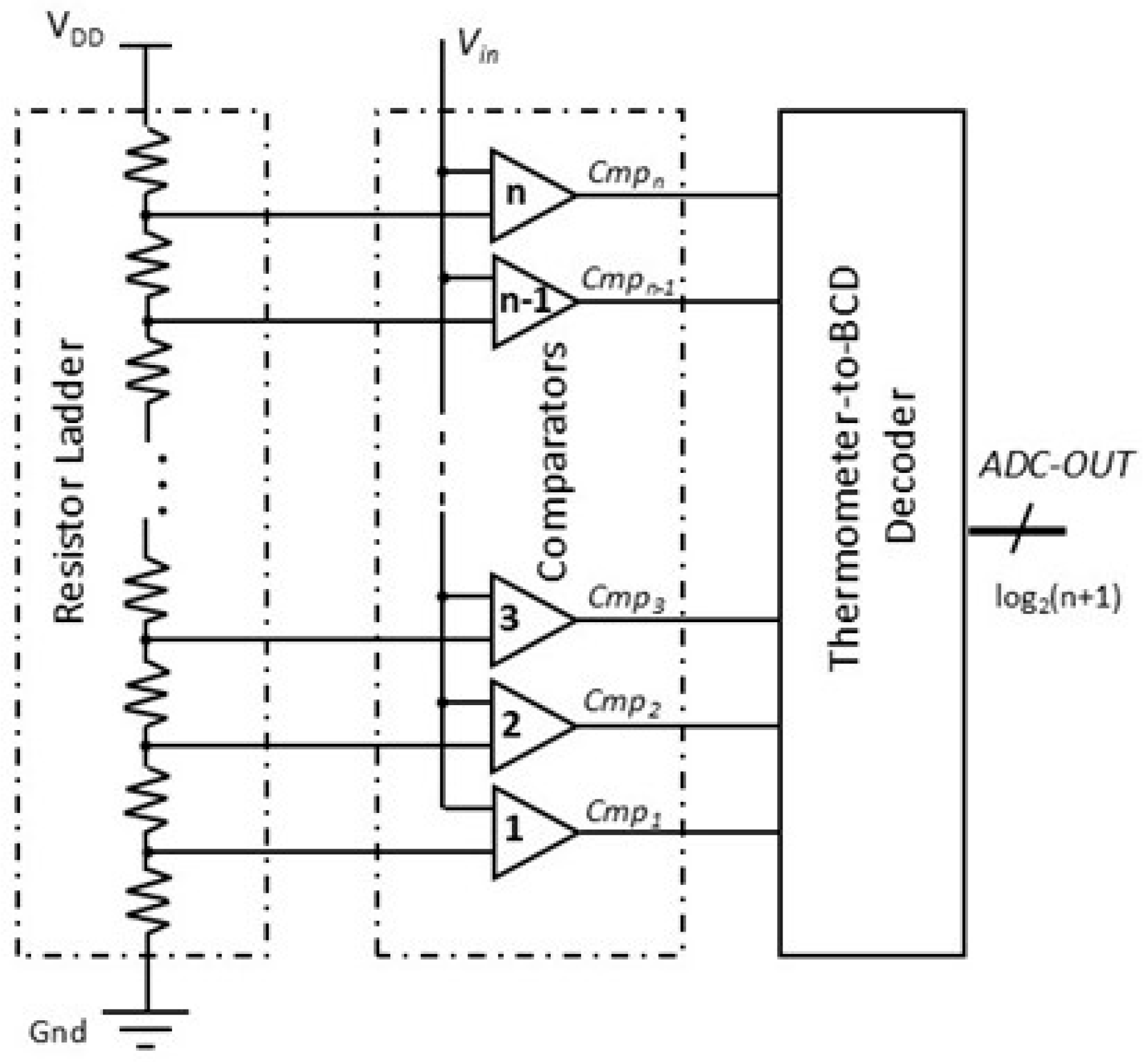
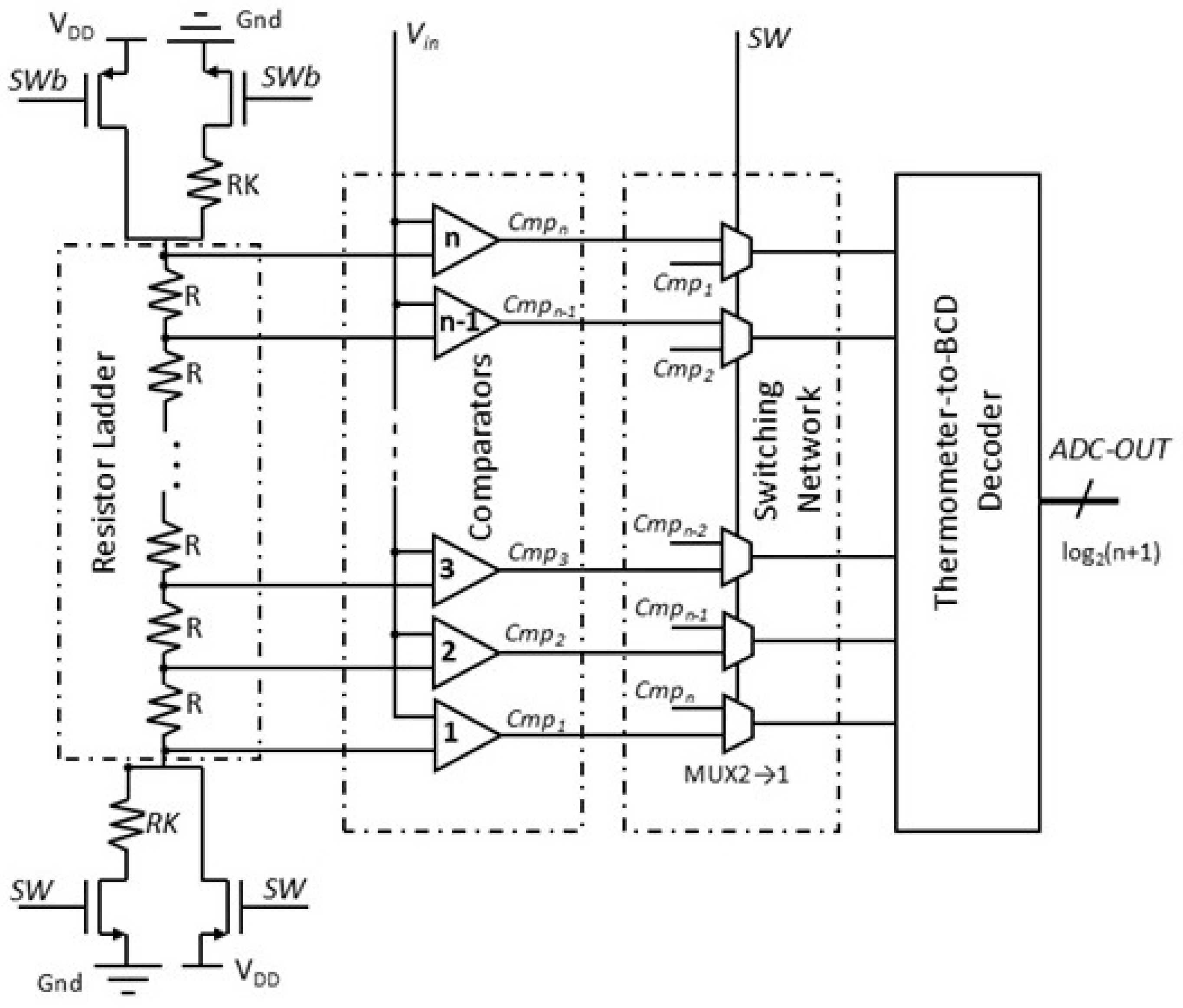
A Flash ADC is a high-speed and efficient circuit for converting an analog signal into a digital representation. The fundamental components of a typical Flash ADC are a resistor ladder network, comparators and a Thermometer-to-BCD code converter [7]. The general topology of a log2(n + 1)-bit Flash ADC is presented in Figure 2, where n is the number of comparators in the design.
The resistor ladder network incorporates a network of serially connected precision resistors (RK = 5 KΩ for fine trimming and R = 1 KΩ for unit steps), and each node produces a unique voltage reference. These resistors divide the power supply voltage into discrete voltage levels to be used as references for the comparators of the converter. Comparators compare the input voltage signal with the reference voltages of the ladder network (one comparator for each reference level). Each comparator determines whether the input voltage is higher or not with respect to its related reference voltage, thereby generating a binary result for each comparison [8]. The comparators’ digital responses are provided in the thermometer code. To attain a Binary-Coded Decimal (BCD) representation of this response, a decoder circuit converts the thermometer code into BCD code, which represents the final digital output of the ADC [9].
Flash ADCs are characterized by high conversion speeds due to the parallel nature of their comparison operation. They can achieve high sampling rates, making them appropriate for applications requiring fast conversion of signals.

3. Influence of BTI-Induced Aging on Flash ADCs

The impact of the BTI-induced aging mechanism on Flash ADC operation is a serious concern, since transistors within the comparators are subjected to permanent stress, which can be either weak or strong [17,18,19]. Considering the topology of the typical Flash ADC, shown in Figure 2, we observe that for each comparator, one of its inputs is driven by a constant voltage from the corresponding tap of the ladder. This implies that DC VGS stress (either strong or weak depending on the position of the comparator with respect to the resistor ladder) affects the relevant transistors of the comparator, which induces BTI-related aging. As expected, the ΔVth shift is more pronounced in the transistors on the side of the ladder that experiences permanently higher VGS stress, so their aging is accelerated. In contrast, the other input of the comparators is driven by a varying analog input signal, so the corresponding transistors experience more balanced BTI stress. This leads to uneven ΔVth shifts between the two transistor groups as well as among the transistors of comparators located on opposite sides of the resistor ladder, which significantly impacts the comparator functionality (e.g., offset voltage rise) and, consequently, the reliability of the ADC. Thus, over time, the ADC may generate erroneous responses.
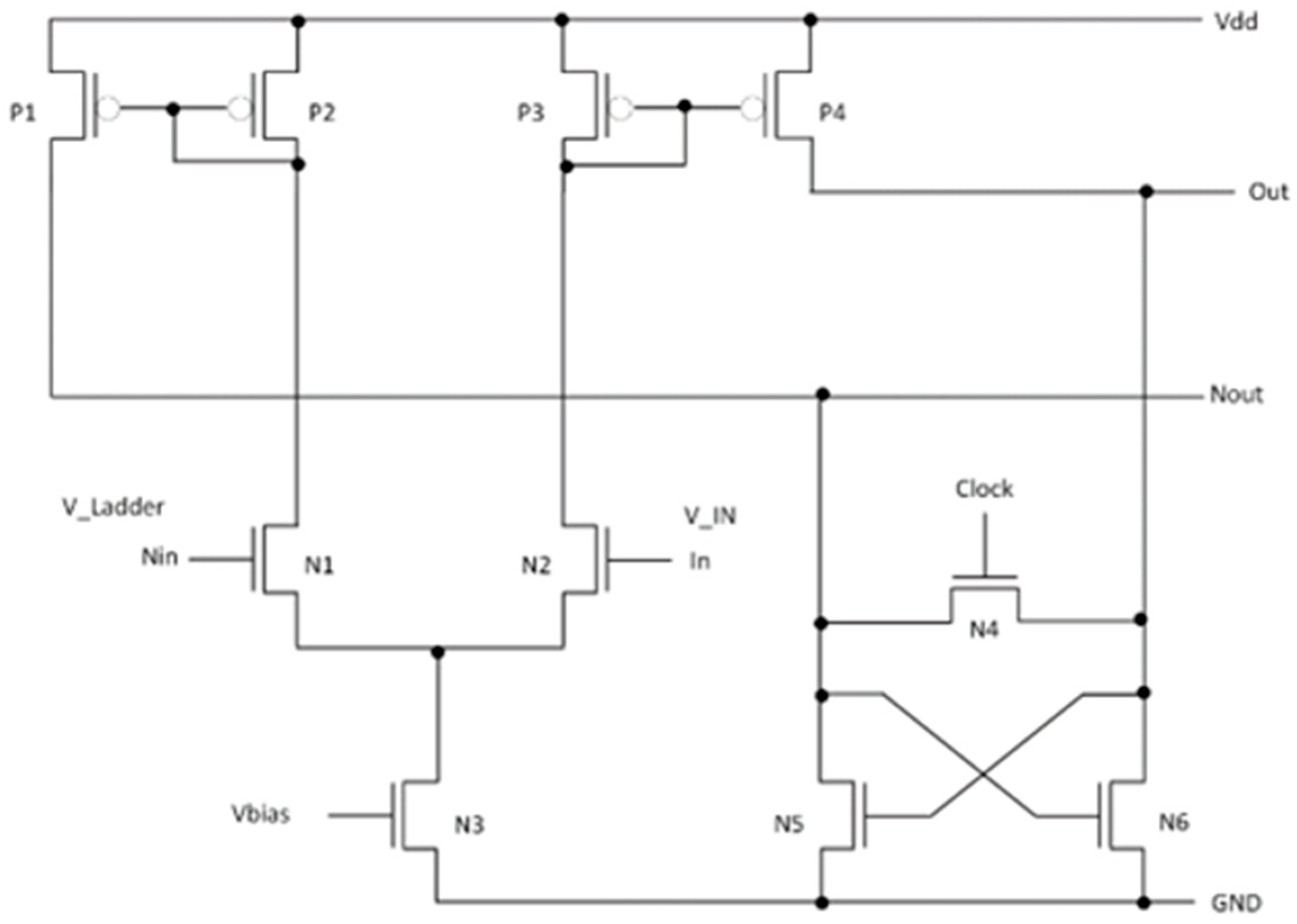
To investigate the effect of BTI-induced aging on comparator transistors in a Flash ADC and validate the proposed mitigation technique, we designed the analog front end of a 4-bit Flash ADC circuit (n = 15), as shown in Figure 2, employing the CMOS 90 nm technology of UMC (SP option–Vdd = 1 V) and using the Virtuoso platform of Cadence. The min and the max reference voltage values of the resistor ladder are 285.1 mV and 887.6 mV, respectively. Without loss of generality, for the scope of this study, the comparator used in the ADC design is shown in Figure 3 [10], with the specific characteristics of the transistors presented in Table 2. It consists of the input differential pair, transistors N1 and N2, along with current mirror loads P1–P2 and P3–P4, respectively. The output currents of the current mirrors are compared using the cross-coupled transistors N5 and N6, and the resulting digital response is latched at the output. The clock signal drives transistor N4 and resets the comparator when this transistor is ON.
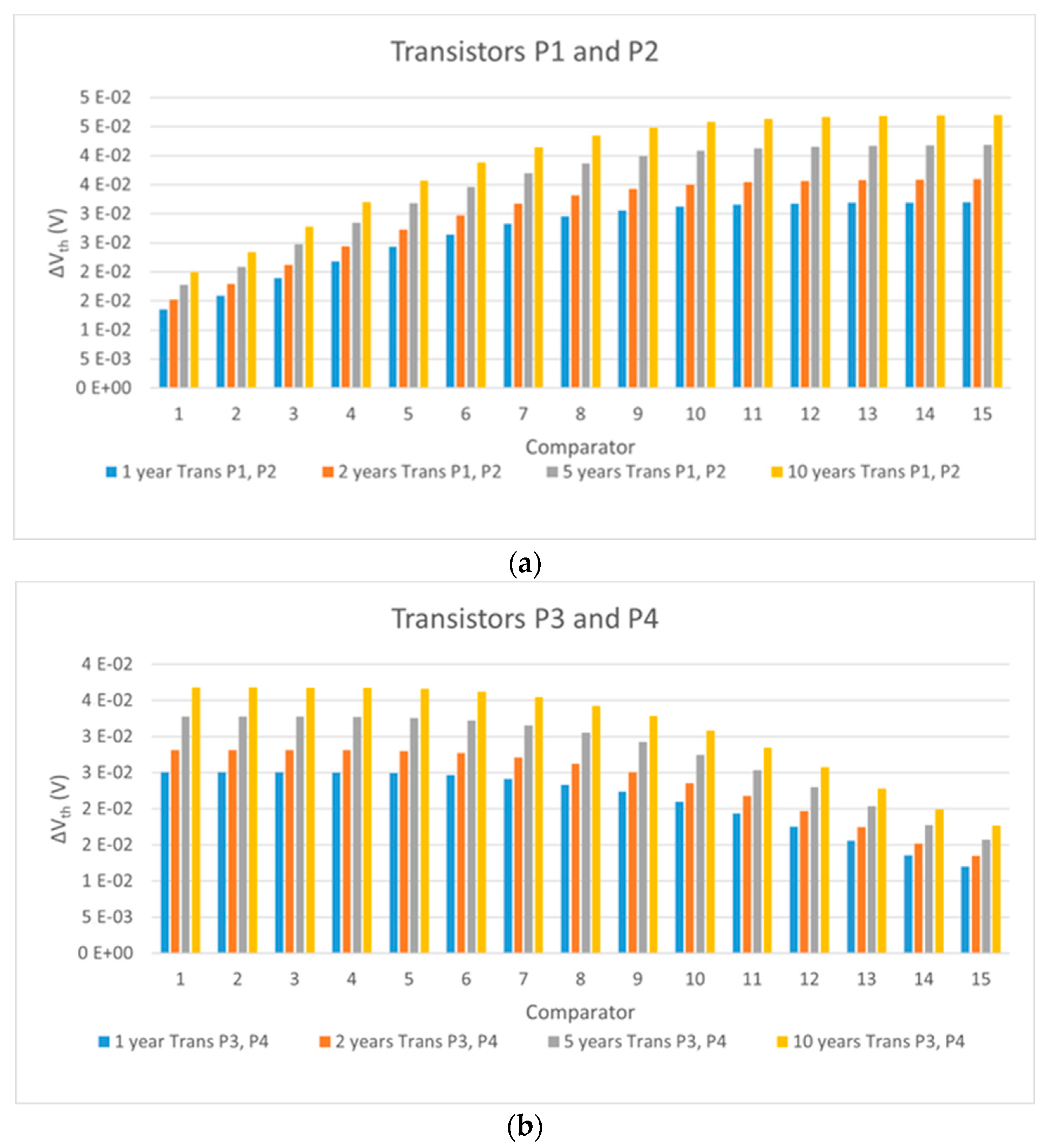
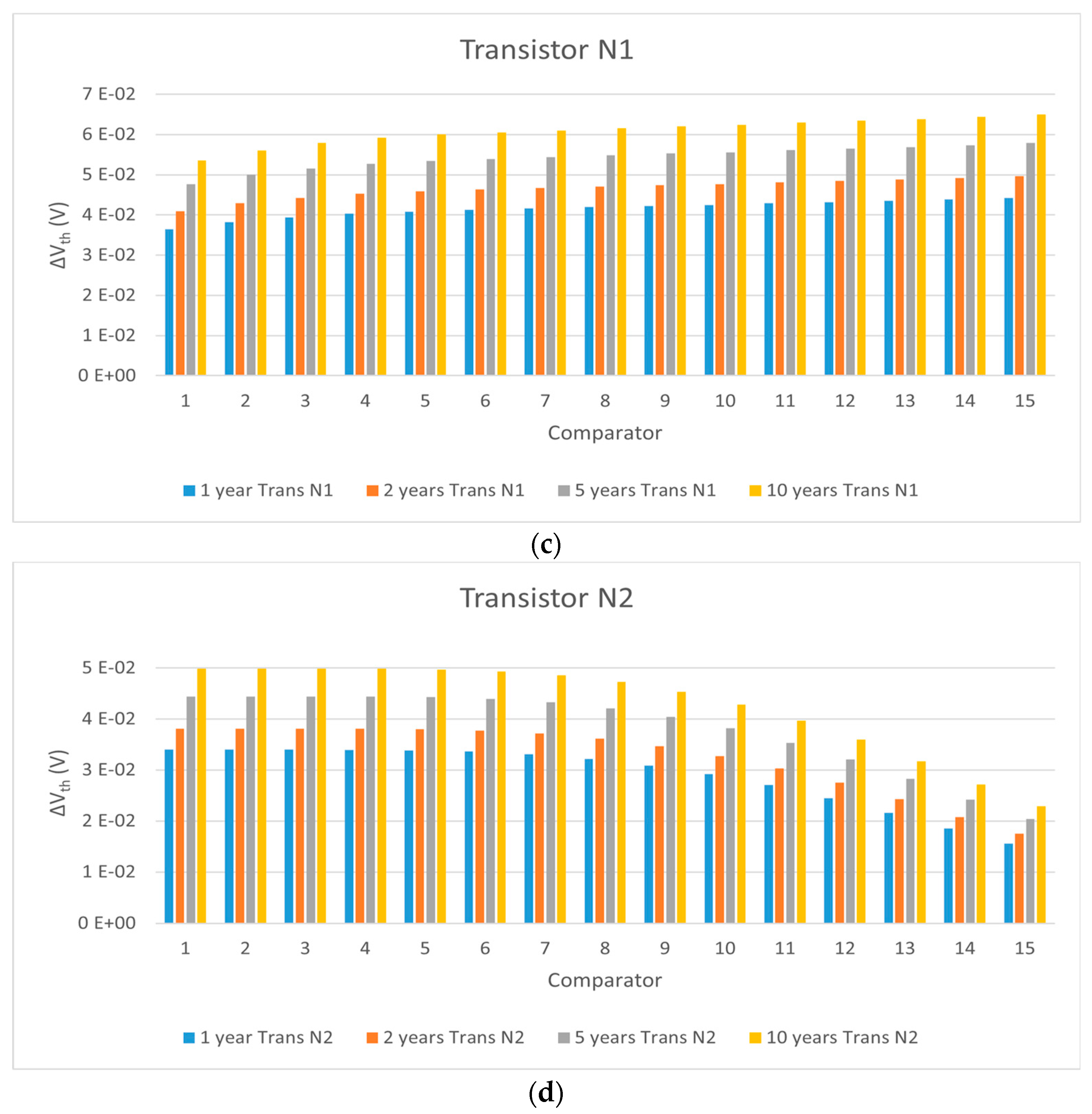
In the simulations, performed using the Spectre platform, the input signal (Vin) that was common to all comparators was set to the mean value of the signal swing (Vmean = 586.35 mV). Exploiting the transistor BTI-induced aging model presented in Sub Section 2.1, the expected ΔVth of the affected transistors in each comparator for the “fresh” (non-aged) state (just after manufacturing), as well as for different operating years, was determined and is presented in Figure 4.
As expected, in the comparators permanently fed by the resistor ladder with higher reference voltage levels (above Vmean), the NMOS input transistors N1 (see Figure 3) are significantly more affected by BTI-induced aging, and their threshold voltage shift becomes higher over time with respect to the relevant transistors of the comparators that are fed with lower reference voltage levels (below Vmean). Moreover, in these cases, NMOS input transistor N1 is more affected by BTI with respect to NMOS input transistor N2, as lower mean VGS levels are statistically expected on transistor N2. A higher influence of BTI is also expected for PMOS transistors P1 and P2 in the left current mirrors than for transistors P3 and P4 of the right current mirrors, as a result of the lower voltage levels of node LN than RN due to the higher conductivity of transistor N1 than N2.
The opposite situation stands for the comparators that are fed with lower reference voltage levels of the ladder (below Vmean). In this case, transistor N2, when driven by the input signal, will present a higher threshold voltage shift over time with respect to transistor N1. Also, transistors P3 and P4 of the right current mirrors will present a higher influence of BTI than transistors P1 and P2 of the left current mirrors, as a result of the statistically lower voltage levels of node RN than LN due to the higher conductivity of transistor N2 than N1. According to the above analysis, transistors P1, P2, N1, and N3 are under constant voltage (VGS) stress conditions, so for the calculation of ΔVth, we set parameter α to 1 in Equation (1). The VGS of transistors P3, P4, and N2 are varied over time so that these transistors experience AC stress, and for the calculation of ΔVth, we set α to 0.25 in Equation (1).
Figure 4 a–d presents the transistors’ threshold voltage shifts in the differential stage of the comparators for various operating times and at a temperature of 125 °C. Note that in each pair of current mirror transistors, P1–P2 and P3–P4, the influence of aging is the same, as both transistors share the same VGS stress.
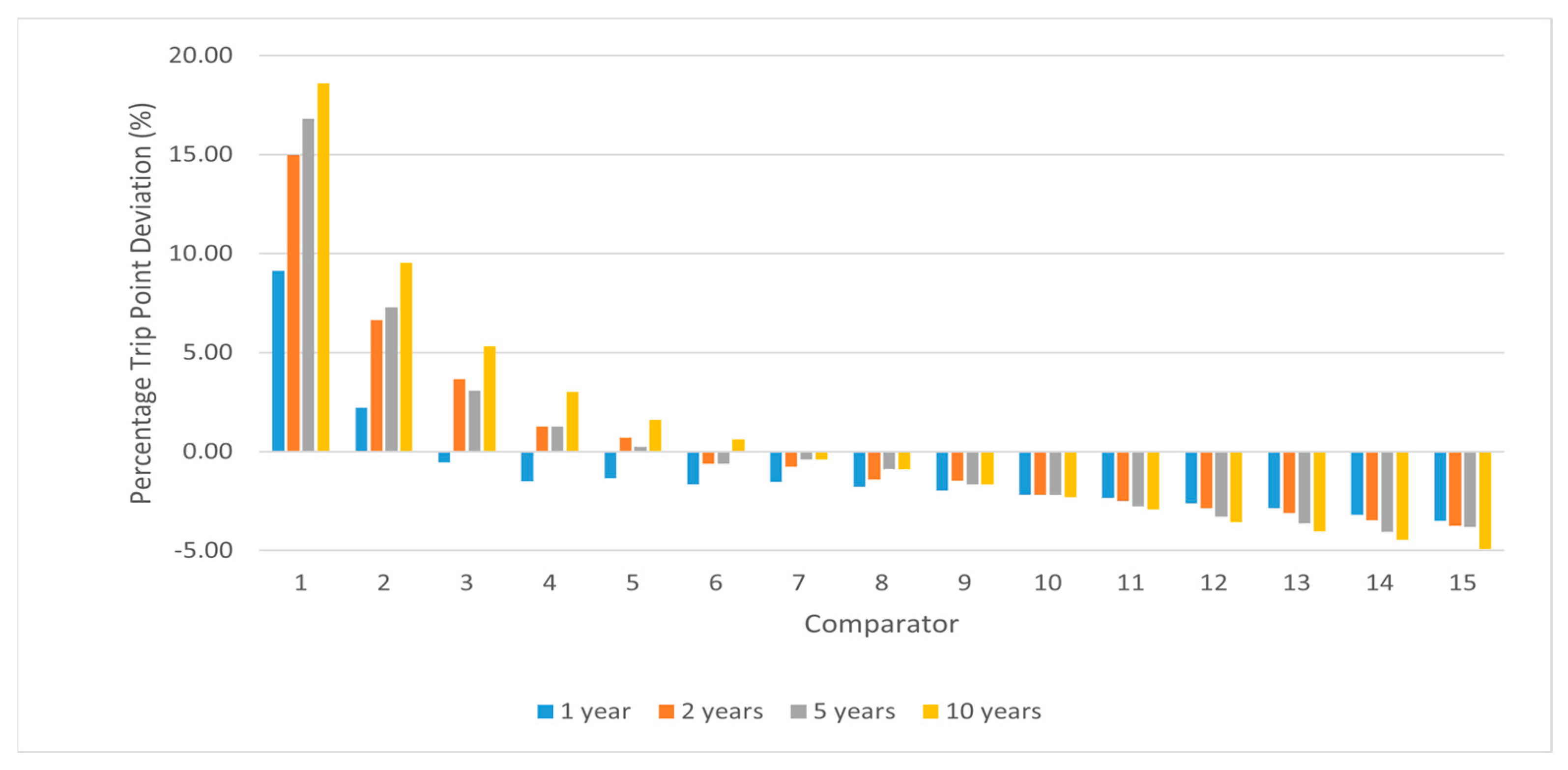
Nevertheless, in both situations above, the unbalanced aging of the transistors at the two branches of the differential stage in each comparator will result in offset generation, which is not identical among the comparators across the ladder. These results are in agreement with those in [17]. Due to this offset, the trip point voltage of each comparator changes over time, as shown in the simulation results of Figure 5, after several years of operation. The trip point voltage of a comparator corresponds to the specific voltage level where the crossing of the input voltage causes its output to switch state. Consequently, we expect that over time, the ADC will provide erroneous responses, leading to drastically reduced reliability.
Note that transistor N3 is biased with a low voltage level (Vbias = 330 mV), so its aging is limited, while it evenly affects both branches of the differential stage. Moreover, transistors N4–N6 of the latch at the output of the comparator are expected to have a very slow aging rate due to the frequent flipping of their state. Thus, transistors N4–N6 are not considered in the aging analysis according to common practice [23].

4. Proposed Aging Mitigation Technique

The goals of the proposed technique for aging mitigation in Flash ADCs are twofold:
  • It initially aims to reduce the aging rate of the comparators’ transistors to extend the circuit’s operating lifetime;
  • In parallel, it intends to equalize transistor aging across all comparators, aiming to homogenize and restrict the offset voltage developed over time due to aging, thereby diminishing trip point shifts and enhancing their reliability.

4.1. Design for Aging Mitigation

The aging mitigation strategy is based on the implementation of a reconfigurable analog front end, where the comparators can periodically exchange their roles with respect to the ladder topology. In more detail, and according to the experimental results in the previous section, we observe that the comparators in the middle of the ladder (comparators 7–9) present a substantially more restrained influence of aging on their trip point voltage with respect to comparators near the two edges of the ladder. For example, comparator 8 presents a relative trip point shift of −0.89%, while comparators 1 and 15 present relative trip point shifts of 18.59% and −4.92%, respectively, after 10 years of operation. Moreover, the trip point shifts of the comparators at the bottom of the ladder (see Figure 2) are positive (increase over time), while the trip point shifts of the comparators at the top of the ladder are negative (decrease overtime). Therefore, symmetrical and periodic switching of the comparators’ roles, with respect to the central comparator (n + 1)/2 (comparator 8 in our design paradigm), was adopted for aging influence mitigation. Thus, the comparators at the two ends of the ladder periodically exchange their roles (comparators 1 and 15 in the paradigm). Consequently, in a periodical manner, the bottom comparator (comparator 1) is fed either with the lowest or the highest reference voltage of the ladder, ladder while the complementary situation stands for the top comparator (comparator 15); in parallel, the immediately adjacent comparators to the previous ones also exchange their roles (e.g., comparators 2 and 14), and this pattern continues up to the pair of comparators (n − 1)/2 and (n + 3)/2 (comparators 7 and 9 in the paradigm). The central comparator (n + 1)/2 (comparator 8 in the design paradigm) remains unaltered.
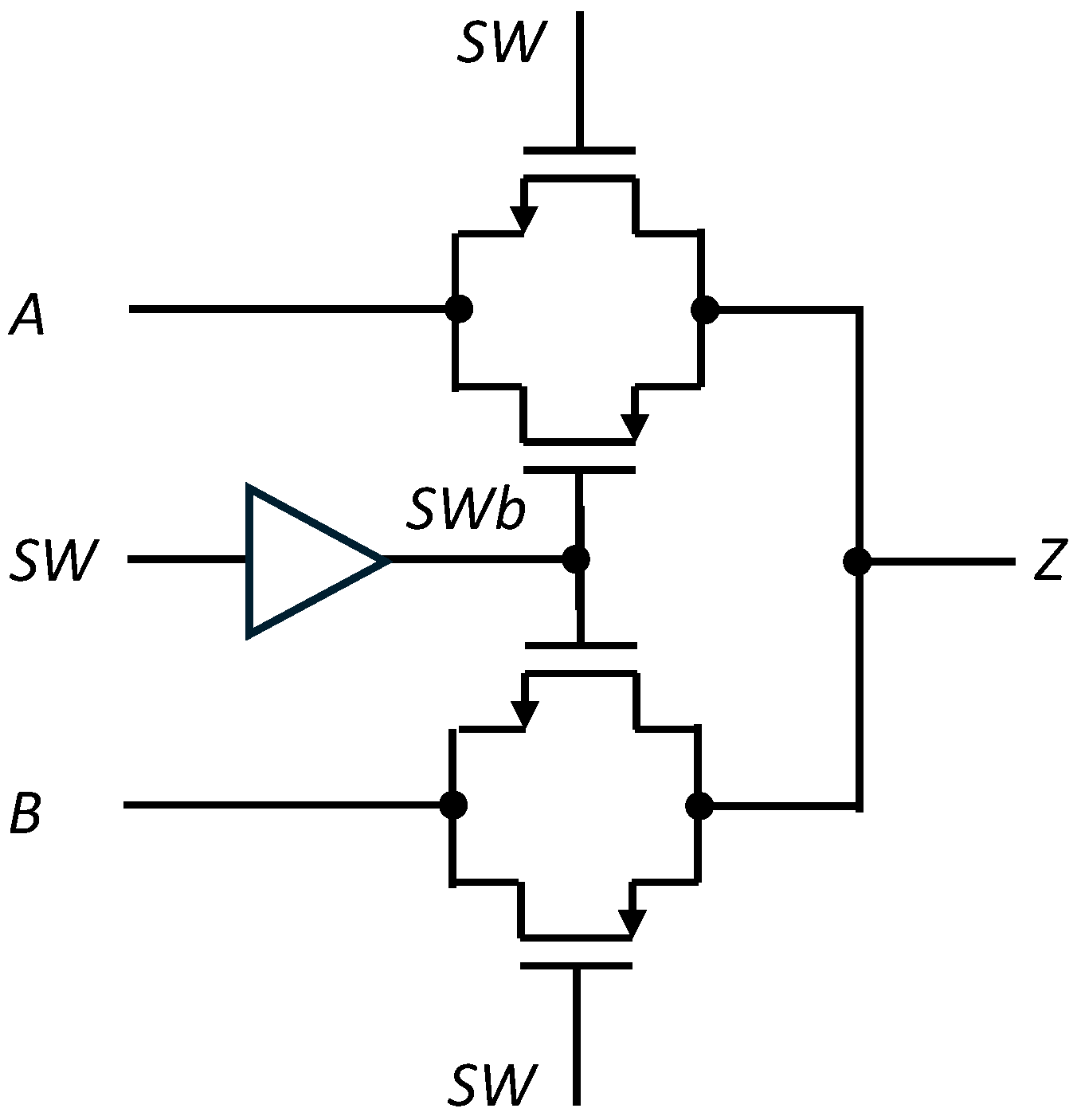
The above aging mitigation technique can be simply implemented by periodically switching the voltage bias at the ladder edges between Vdd and Gnd. A reconfigurable ADC topology is adopted where four extra transistors are required; a pair of PMOS-NMOS transistors at each edge (bottom and top) of the ladder topology, as shown in Figure 6. Table 3 presents the characteristics of these transistors. The bottom transistors are controlled by the signal SW, while the top ones are controlled by its complementary signal SWb. In order to switch the ladder between the two states, the ADC operation is halted for just one clock cycle after quite a large number of cycles between two aging mitigation actions, so that in practice no influence on its throughput is expected. Moreover, this modification at the ladder side must be followed by the addition of a switching network (a network of (n − 1) 2-to-1 multiplexers composed of simple pass gates) between the comparators and the Thermometer-to-BCD Decoder, as illustrated in Figure 6. Figure 7 illustrates the proposed 2-to-1 multiplexer implemented in the switching network, and Table 4 presents the relevant transistors’ characteristics. All multiplexers are controlled by the SW signal. Thus, in every state of circuit operation, each comparator feeds the correct input of the Thermometer-to-BCD Decoder according to its role with respect to the ladder’s state of operation.
Considering the simulation results that follow, by adopting the above technique, it is feasible to mitigate uneven transistor aging in the comparators and achieve more uniform transistor Vth degradation across all comparators while in parallel slowing down the Vth degradation of highly stressed comparators. Thus, for each comparator the deviation of the trip point from the expected value is reduced so that the influence of BTI-induced aging on the ADC performance characteristics is restricted.

4.2. Simulation Results on Aging Mitigation

The proposed aging mitigation technique is applied in the design of the 4-bit Flash ADC under consideration, as shown in Figure 6. For the estimation of the evolution of the threshold voltage shift over time, we recursively apply Equation (1) for each transistor of each comparator and for each periodic ladder state, using as the initial Vth value of the current state the final Vth value of the previous state, and this pattern continues until the process is complete. Thus, we sequentially accumulate the incremental ΔVth predicted for each device at successive τ periods. This approach ensures continuity and yields a representative mid-stress evolution.
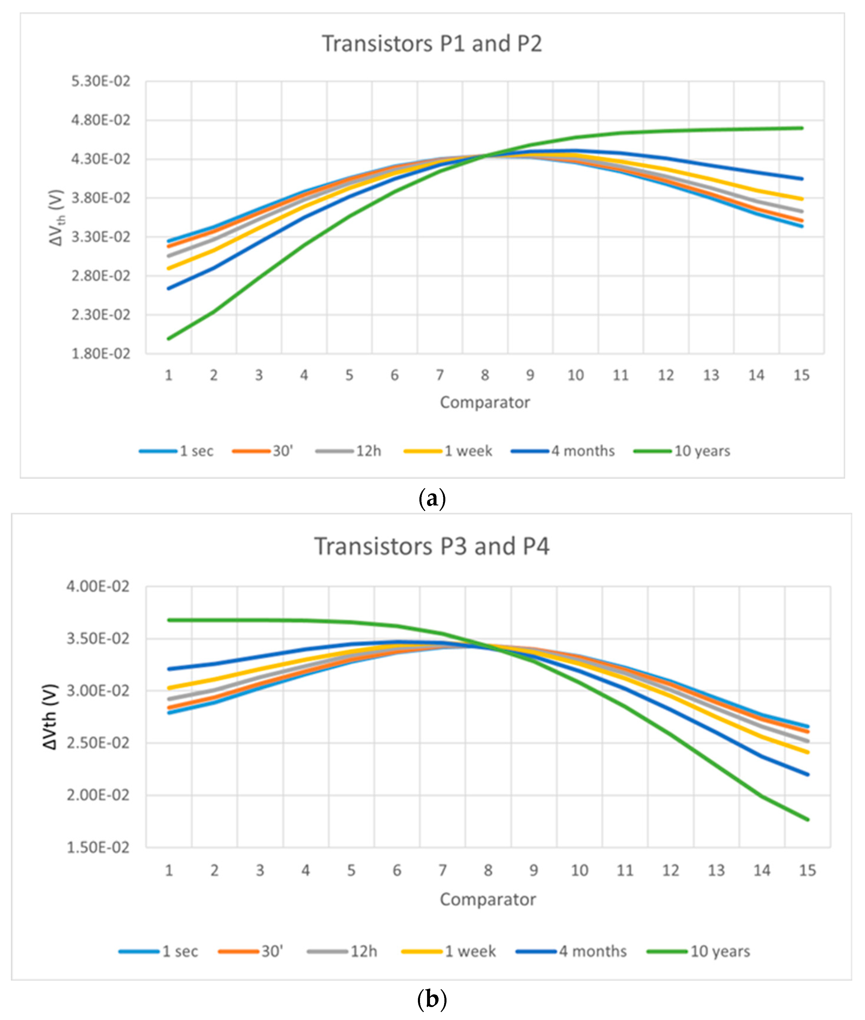
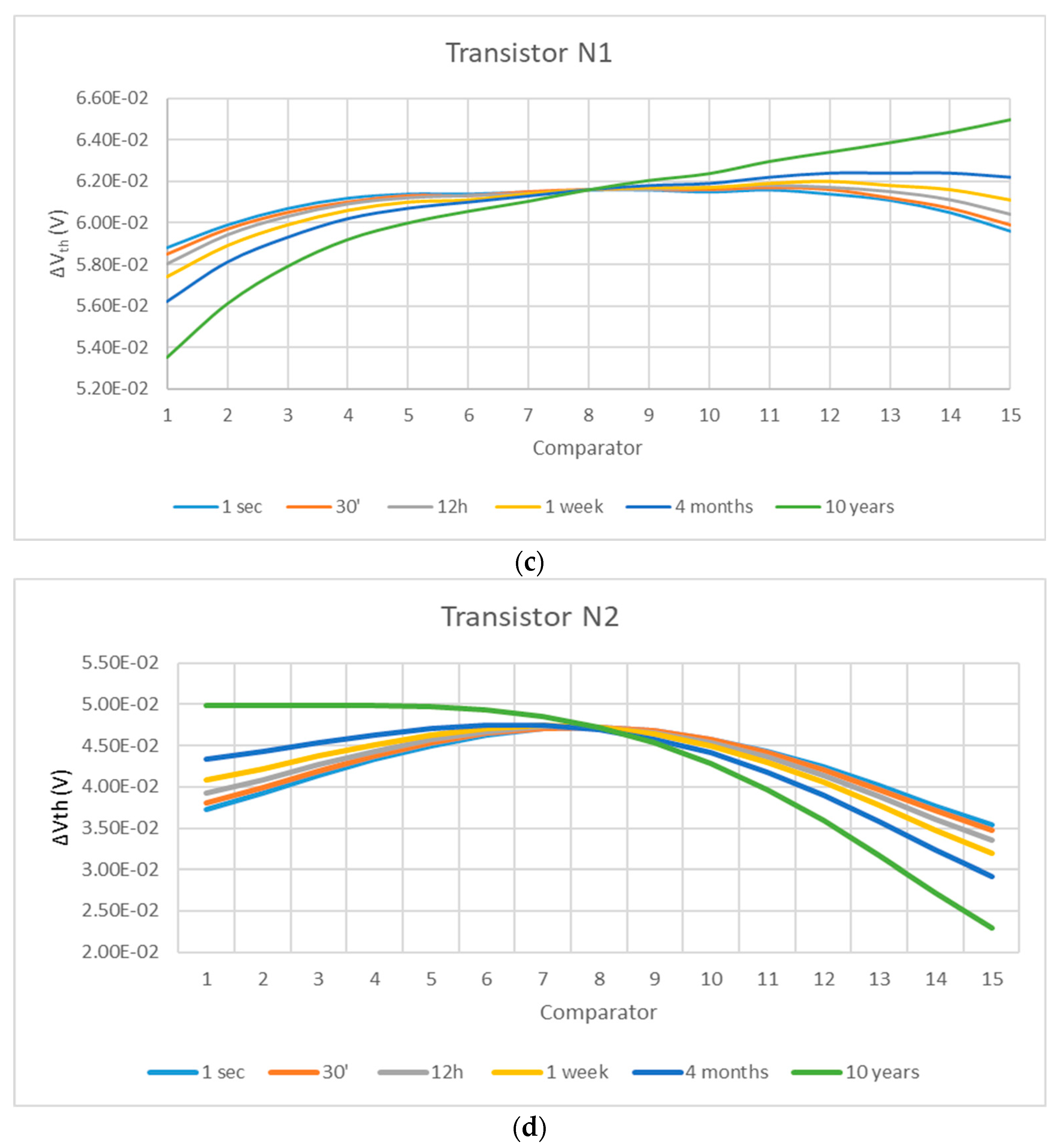
In Figure 8, we present the evolution of the transistors’ threshold voltage shifts in each comparator due to aging, after ten years of operation and under various resistor ladder switching rates, ranging from one switch per 1 s, 30 min, 12 h, 1 week and 4 months. For comparisons, the transistors’ threshold voltage shifts after 10 years of operation without any resistor ladder switching activity (typical stress conditions) are also illustrated in this figure.
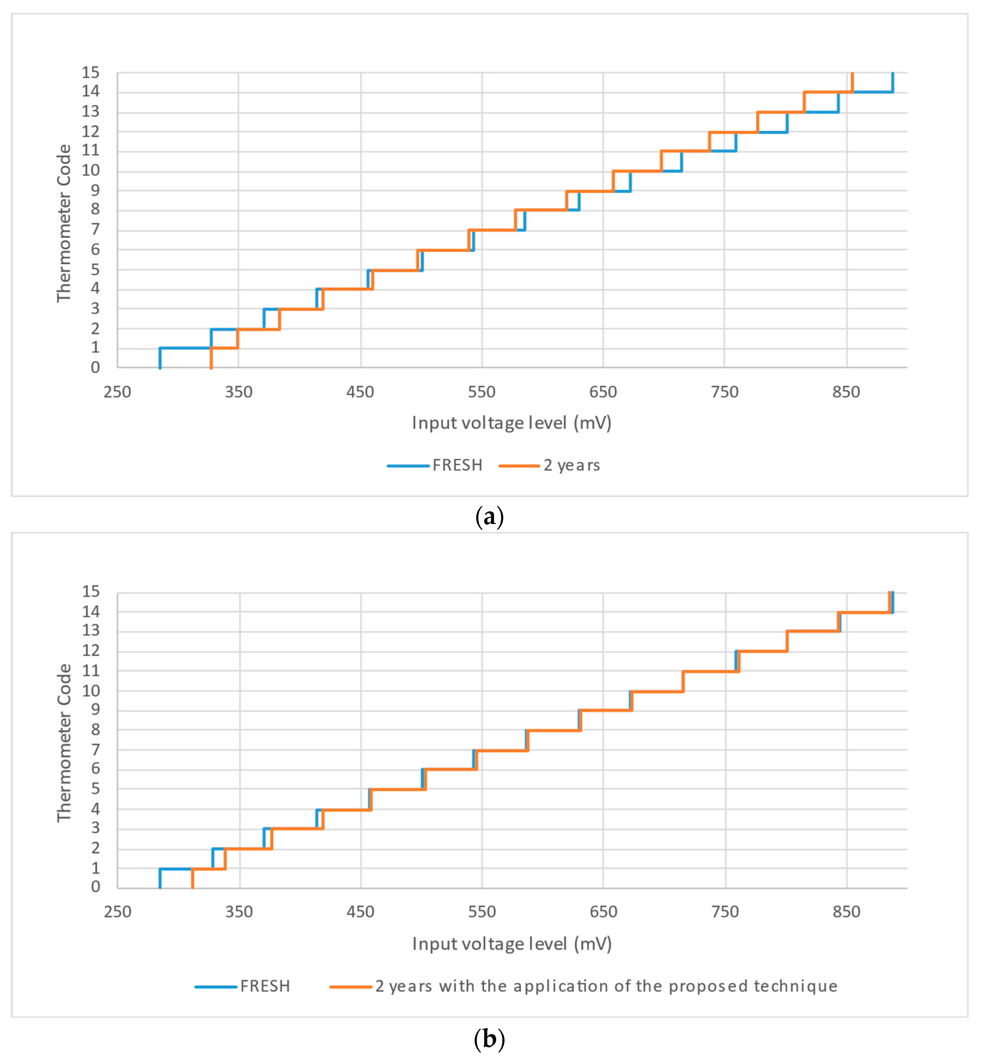
We observe that by increasing the switching rate, the threshold voltage shift tends to homogenize among the corresponding transistors in the comparators. This is indicated by the tendency of the curve to become flat as the switching rate increases. Thus, for those transistors in the comparators that are highly stressed in the original ADC design (without switching activity), the application of the proposed aging mitigation technique results in a reduced total threshold voltage shift. The opposite stands for the transistors experiencing low stress, where the total threshold voltage shift is increased when the new technique is applied. Overall, and according to Figure 8, the application of the proposed technique results in balanced threshold voltage degradation across the respective transistors of all comparators, and in parallel between the corresponding transistors in the two branches of each comparator. As a consequence, this balanced threshold voltage degradation substantially restricts the deviation of the comparators’ trip point from the expected value, according to the simulation results in Figure 9 and Figure 10.
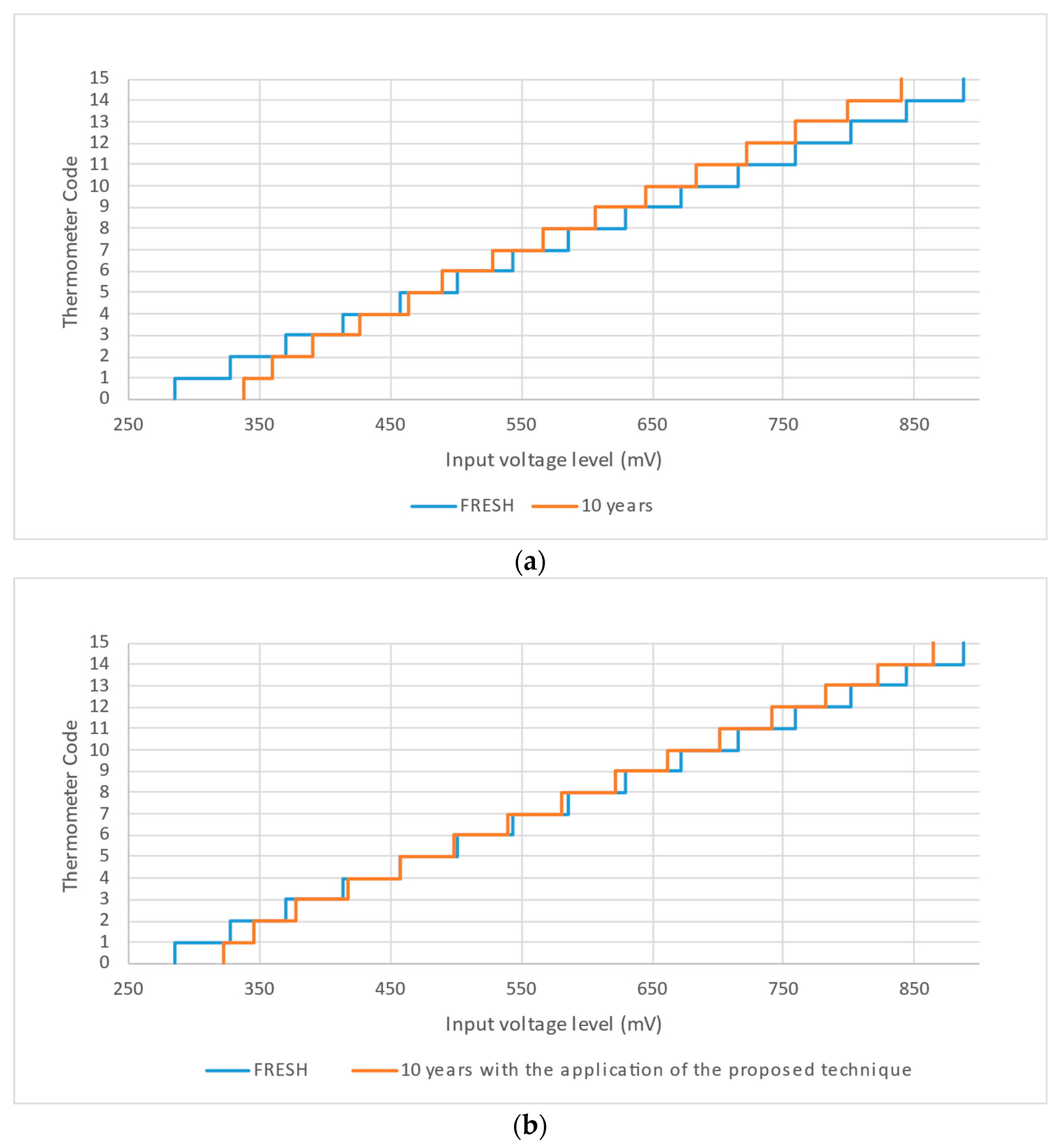
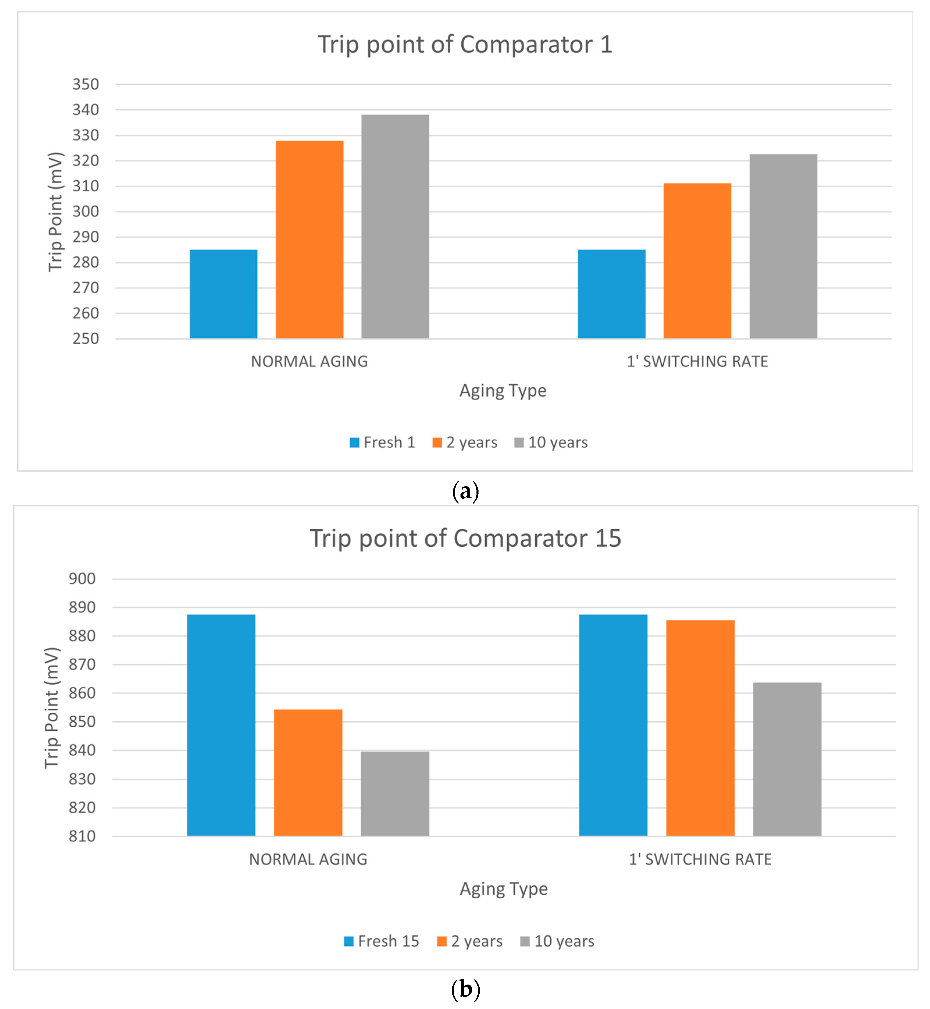
Both figures present the response characteristic of the ADC circuit in the “fresh” (non-aged) condition and after two and ten years of operation, respectively, without and with the application of the proposed aging mitigation technique. In these curves, it is easy to observe the trip point shift of the comparators over the years and its significant reduction after the application of the proposed aging mitigation technique. For example, in Figure 10a, after ten years of operation without applying the proposed technique, a significant trip point deviation appears in all comparators, with the highest values obtained for comparator 1 (53.1 mV, which corresponds to a 18.63% deviation) and comparator 15 (47.9 mV, which corresponds to a 5.4% deviation), as also illustrated in Figure 11. On the contrary, using the aging mitigation technique, after ten years of operation, the trip point deviation is drastically reduced, and in comparator 5, it is almost eliminated. According to Figure 11, for comparator 1 the trip point deviation reduces to 37.5 mV (a reduction of 29.37%), while for comparator 15 it reduces to 23.9 mV (a reduction of 54.99%).
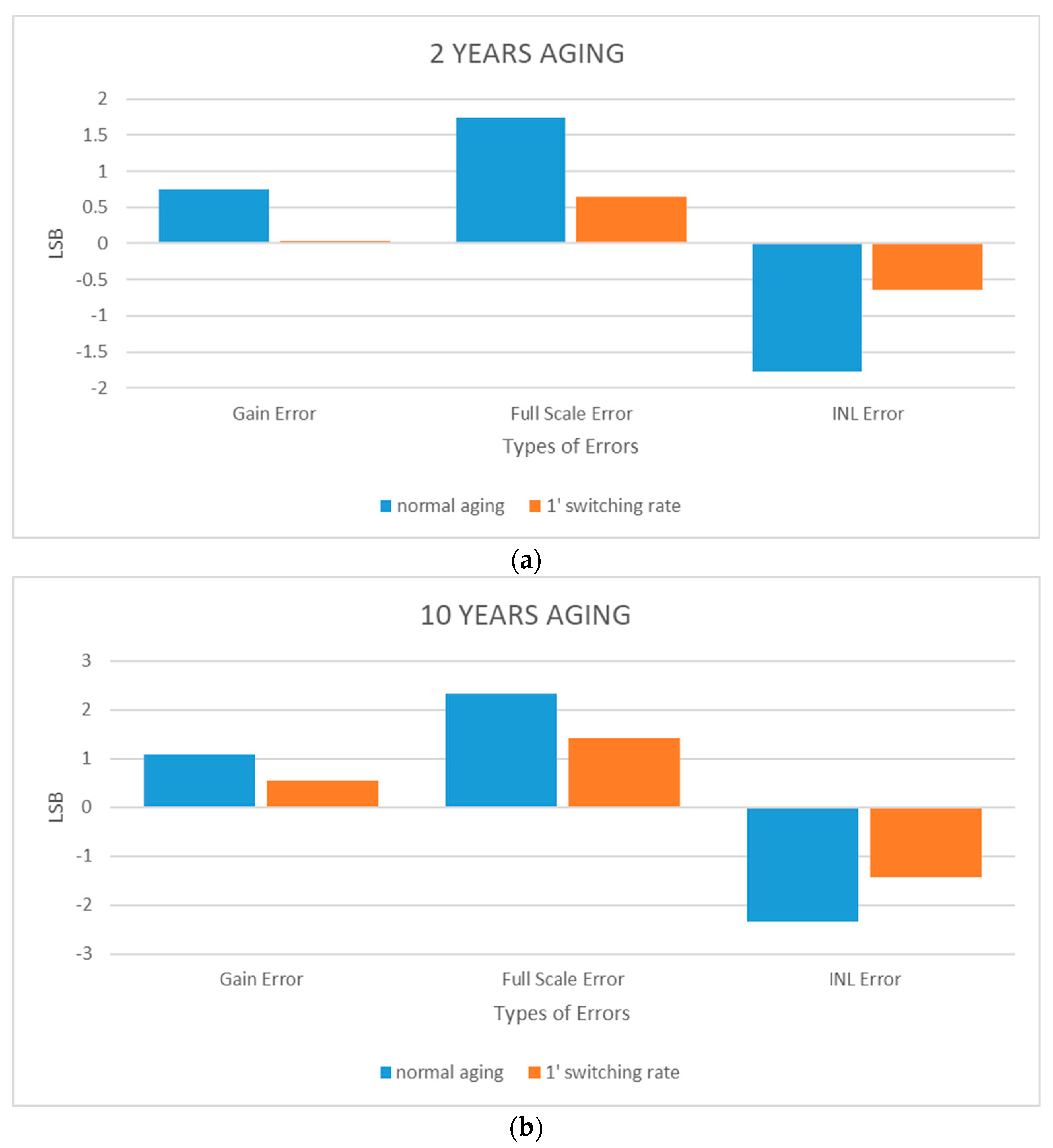
Obviously, the influence of aging on the comparators’ trip point also affects, as a side effect, the ADC performance metrics (gain, full-scale error, integral nonlinearity (INL)). Thus, by reducing the aging-induced trip point deviation of the comparators, the ADC performance metrics are improved. In Figure 12, the reductions in the aging-related gain, and in the full-scale and INL errors, achieved by applying the proposed technique (with a switching period of 1 s), after 2 and 10 years of operation are presented. The gain error reductions are 95.54% and 50.65% after 2 and 10 years of operation, respectively. In addition, for the same operating times, the full-scale error reductions are 63.31% and 39.32%, and the INL error reductions are 63.00% and 39.21%, respectively.

5. Conclusions

In this paper we investigate the impact of transistor BTI-induced aging on the analog front end of Flash ADCs, and we propose an aging mitigation technique aiming to retain the ADC’s performance and extend its operating lifetime. BTI-induced aging crucially affects the offset voltage of the used comparators and, consequently, their trip point voltage. In turn, the ADC performance characteristics, such as gain, full-scale error and integral nonlinearity, are also affected.
The proposed BTI-induced aging mitigation technique is based on a simple and low-silicon-area-cost circuit reconfiguration mechanism that periodically alters comparators’ functionality, reducing the average voltage stress on their transistors. As a result, the comparators’ offset voltage development is restricted, and the same stands for the shift in their trip point voltage. Thus, the impact of aging on the ADC performance characteristics is drastically reduced, ensuring long-term reliable operation. For two years of circuit operation, the ADC with the application of the proposed aging mitigation technique presents a gain error reduction of 95.43%, full-scale error reduction of 63.31% and integral nonlinearity reduction of 63.00%, with respect to the original ADC. Finally, note that the silicon area overhead of the proposed solution is only four transistors on the resistor ladder side and one digital 2-to-1 multiplexer at the output of each comparator, plus a control signal.

Author Contributions

Conceptualization, K.M. and Y.T.; methodology, K.M., H.-M.D. and Y.T.; validation, K.M. and H.-M.D.; formal analysis, K.M., H.-M.D. and Y.T.; investigation, K.M. and Y.T.; resources, K.M. and H.-M.D.; writing—original draft preparation, K.M.; writing—review and editing, H.-M.D. and Y.T.; visualization, K.M.; supervision, Y.T. All authors have read and agreed to the published version of the manuscript.

Funding

This research received no external funding.

Institutional Review Board Statement

Not applicable.

Informed Consent Statement

Not applicable.

Data Availability Statement

The original contributions presented in this study are included in the article. Further inquiries can be directed to the corresponding author.

Conflicts of Interest

The authors declare no conflicts of interest.

References

  1. Maricau, E.; Gielen, G. Analog IC Reliability in Nanometer CMOS; Springer: New York, NY, USA, 2013. [Google Scholar]
  2. Reis, R.; Cao, Y.; Wirth, G. Circuit Design for Reliability; Springer: New York, NY, USA, 2015. [Google Scholar]
  3. Panagopoulos, G.D. Variability and Reliability Issues in Mixed-Signal Circuits. In Mixed-Signal Circuits; CRC Press: Boca Raton, FL, USA, 2015; pp. 95–125. [Google Scholar]
  4. Park, G.; Kim, M.; Kim, C.H.; Kim, B.; Reddy, V. All-Digital PLL Frequency and Phase Noise Degradation Measurements Using Simple on-Chip Monitoring Circuits. In Proceedings of the 2018 IEEE International Reliability Physics Symposium (IRPS), Burlingame, CA, USA, 11–15 March 2018. [Google Scholar] [CrossRef]
  5. Dhar, T.; Sapatnekar, S.S. Reliability Analysis of a Delay-Locked Loop Under HCI and BTI Degradation. In Proceedings of the IEEE International Reliability Physics Symposium (IRPS), Monterey, CA, USA, 31 March–4 April 2019; pp. 1–6. [Google Scholar]
  6. Reddy, V.; Martin, S.; Benaissa, K.; Chancellor, C.; Bhatia, K.; Srinivasan, V.; Rentala, V.; Krishnan, S.; Ondrusek, J. Challenges in Radio Frequency and Mixed-Signal Circuit Reliability. In Proceedings of the IEEE International Electron Devices Meeting (IEDM), San Francisco, CA, USA, 7–11 December 2019. [Google Scholar] [CrossRef]
  7. Khan, M.A.; Kerkhoff, H.G. An Indirect Technique for Estimating Reliability of Analog and Mixed-Signal Systems during Operational Life. In Proceedings of the IEEE 16th International Symposium on Design and Diagnostics of Electronic Circuits & Systems (DDECS), Karlovy Vary, Czech Republic, 7–11 April 2013; pp. 159–164. [Google Scholar]
  8. Aragones, X.; Barajas, E.; Crespo-Yepes, A.; Mateo, D.; Rodriguez, R.; Martin-Martinez, J.; Nafria, M. Aging in CMOS RF Linear Power Amplifiers: An Experimental Study. IEEE Trans. Microw. Theory Tech. 2021, 69, 1453–1463. [Google Scholar] [CrossRef]
  9. Chouard, F.R.; More, S.; Fulde, M.; Schmitt-Landsiedel, D. An Aging Suppression and Calibration Approach for Differential Amplifiers in Advanced CMOS Technologies. In Proceedings of the ESSCIRC (ESSCIRC), Helsinki, Finland, 12–16 September 2011; pp. 251–254. [Google Scholar]
  10. Bhattacharjee, A.; Pradhan, S.N. Impact of Transistor Aging on the Reliability of the Analog Circuit. In Proceedings of the International Conference on Computational Performance Evaluation (ComPE), Shillong, India, 2–4 July 2020; pp. 212–216. [Google Scholar]
  11. Afacan, E.; Dündar, G.; Başkaya, F.; Pusane, A.E.; Yelten, M.B. On Chip Reconfigurable CMOS Analog Circuit Design and Automation Against Aging Phenomena: Sense and React. ACM Trans. Des. Autom. Electron. Syst. 2019, 24, 1–22. [Google Scholar] [CrossRef]
  12. Wan, J.; Kerkhoff, H.G. Reliability of SAR ADCs and Associated Embedded Instrument Detection. In Proceedings of the IEEE 20th International Mixed-Signals Testing Workshop (IMSTW), Paris, France, 24–26 June 2015; pp. 1–5. [Google Scholar]
  13. Lajmi, R.; Cacho, F.; David, O.; Blanc, J.-P.; Rouat, E.; Haendler, S.; Benech, P.; Larroze, E.L.; Bourdel, S. Reliability Assessment of 4GSP/s Interleaved SAR ADC. In Proceedings of the IEEE International Reliability Physics Symposium (IRPS), Burlingame, CA, USA, 11–15March 2018; pp. P-CR.5-1–P-CR.5-6. [Google Scholar]
  14. Choi, W.H.; Kim, H.; Kim, C.H. Circuit Techniques for Mitigating Short-Term Vth Instability Issues in Successive Approximation Register (SAR) ADCs. In Proceedings of the IEEE Custom Integrated Circuits Conference (CICC), San Jose, CA, USA, 28–30 September 2015; pp. 1–4. [Google Scholar]
  15. Park, G.; Kim, M.; Pande, N.; Chiu, P.-W.; Song, J.; Kim, C.H. A Counter Based ADC Non-Linearity Measurement Circuit and Its Application to Reliability Testing. In Proceedings of the IEEE Custom Integrated Circuits Conference (CICC), Austin, TX, USA, 14–17 April 2019; pp. 1–4. [Google Scholar]
  16. Sharara, L.; Navidi, S.M.; Al Maharmeh, H.; Parekh, S.; Wehbi, A.; Alhawari, M.; Ismail, M. Analysis and Effects of Aging and Electromigration on Mixed-Signal ICs in 22nm FDSOI Technology. In Proceedings of the 29th IEEE International Conference on Electronics, Circuits and Systems (ICECS), Glasgow, UK, 24–26 October 2022; pp. 1–4. [Google Scholar]
  17. Gielen, G.; Maricau, E. Stochastic Degradation Modeling and Simulation for Analog Integrated Circuits in Nanometer CMOS. In Proceedings of the Design, Automation & Test in Europe Conference & Exhibition (DATE), Grenoble, France, 18–22 March 2013; pp. 326–331. [Google Scholar]
  18. Simicic, M.; Weckx, P.; Parvais, B.; Roussel, P.; Kaczer, B.; Gielen, G. Understanding the Impact of Time-Dependent Random Variability on Analog ICs: From Single Transistor Measurements to Circuit Simulations. IEEE Trans. Very Large Scale Integr. VLSI Syst. 2019, 27, 601–610. [Google Scholar] [CrossRef]
  19. Xu, X.; Li, M.; Shi, Y.; Li, Y.; Zhu, H.; Sun, Q. Aging Analysis and Anti-Aging Circuit Design of Strong-Arm Latch Circuits in 14 Nm FinFET Technology. Electronics 2025, 14, 772. [Google Scholar] [CrossRef]
  20. Omana, M.; Rossi, D.; Edara, T.; Metra, C. Impact of Aging Phenomena on Latches’ Robustness. IEEE Trans. Nanotechnol. 2016, 15, 129–136. [Google Scholar] [CrossRef]
  21. Toledano-Luque, M.; Kaczer, B.; Franco, J.; Roussel, P.J.; Grasser, T.; Hoffmann, T.Y.; Groeseneken, G. From Mean Values to Distributions of BTI Lifetime of Deeply Scaled FETs through Atomistic Understanding of the Degradation. In Proceedings of the Symposium on VLSI Technology–Digest of Technical Papers, Kyoto, Japan, 14–16 June 2011; pp. 152–153. [Google Scholar]
  22. Singh, H.; Mahmoodi, H. Analysis of SRAM Reliability under Combined Effect of NBTI, Process and Temperature Variations in Nano-Scale CMOS. In Proceedings of the 5th International Conference on Future Information Technology, Busan, Republic of Korea, 21–23 February 2010; pp. 1–4. [Google Scholar]
  23. Ahmed, F.; Milor, L. Online Measurement of Degradation Due to Bias Temperature Instability in SRAMs. IEEE Trans. Very Large Scale Integr. VLSI Syst. 2016, 24, 2184–2194. [Google Scholar] [CrossRef]
Figure 1. BTI modeling of (a) NBTI and (b) PBTI for the simulations.
Chips 04 00036 g001
Figure 2. Typical topology of a Flash ADC.
Chips 04 00036 g002
Figure 3. The comparator under consideration [10].
Chips 04 00036 g003
Figure 4. Transistors’ threshold voltage shifts: (a) transistors P1 and P2; (b) transistors P3 and P4; (c) transistor N1; (d) transistor N2.
Chips 04 00036 g004aChips 04 00036 g004b
Figure 5. Comparators’ relative trip point voltage deviations.
Chips 04 00036 g005
Figure 6. Proposed Flash ADC aging mitigation topology.
Chips 04 00036 g006
Figure 7. Proposed 2-1 multiplexer.
Chips 04 00036 g007
Figure 8. Transistors’ threshold voltage shifts in the comparators at various switch rates of the proposed aging mitigation mechanism at 10 years of operation: (a) transistors P1 and P2; (b) transistors P3 and P4; (c) transistor N1; (d) transistor N2.
Chips 04 00036 g008aChips 04 00036 g008b
Figure 9. ADC response characteristics after two years of operation: (a) without and (b) with the application of the proposed aging mitigation technique (switching rate of 1 s).
Chips 04 00036 g009
Figure 10. ADC response characteristics after ten years of operation: (a) without and (b) with the application of the proposed aging mitigation technique (switching rate of 1 s).
Chips 04 00036 g010
Figure 11. Trip point voltage deviation for (a) comparator 1 and (b) comparator 15 after 2 and 10 years of operation, without and with the application of the proposed mitigation technique (switching rate of 1 s).
Chips 04 00036 g011
Figure 12. Evaluation of ADC gain, full-scale error and INL performance characteristics, without and with the proposed technique (switching rate of 1 s) after (a) 2 and (b) 10 years of operation.
Chips 04 00036 g012
Table 1. Technological features used in Equations (1) and (2).
Vdd = 1 VESPOX = 3.9
nMOS TransistorspMOS Transistors
Nominal threshold voltageVth0n = 1 mVVth0p = 58.1 mV
Carrier mobilityUon = 0.23 m2/(V·s)Uop = 9.26 m2/(V·s)
Gate oxide thicknessToxn = 2.25 nmToxp = 2.45 nm
Table 2. Comparator transistors’ characteristics.
nMOS TransistorspMOS Transistors
Length = 160 nmLength = 160 nm
Width = 720 nmWidth = 720 nm
Bulk @ GNDBulk @ Vdd
Table 3. Ladder transistors’ characteristics.
nMOS TransistorspMOS Transistors
Length = 160 nmLength = 160 nm
Width = 2 μmWidth = 2 μm
Bulk @ GNDBulk @ Vdd
Table 4. The 2-to-1 multiplexer transistors’ characteristics.
nMOS TransistorspMOS Transistors
Length = 80 nmLength = 80 nm
Width = 240 nmWidth = 120 nm
Bulk @ GNDBulk @ Vdd
Disclaimer/Publisher’s Note: The statements, opinions and data contained in all publications are solely those of the individual author(s) and contributor(s) and not of MDPI and/or the editor(s). MDPI and/or the editor(s) disclaim responsibility for any injury to people or property resulting from any ideas, methods, instructions or products referred to in the content.