Article

Deep Learning Study on Memory IC Package Warpage Using Deep Neural Network and Finite Element Simulation

1
Micron Technology Operations India LLP., Survey No. 115/35, Hyderabad 500032, Telangana, India
2
Micron Semiconductor Asia Operations Pte. Ltd., 990, Bendemeer Road, Singapore 339942, Singapore
3
Micron Technology, Inc., 8000 South Federal Way, Boise, ID 83716, USA
*
Author to whom correspondence should be addressed.
Chips 2025, 4(3), 35; https://doi.org/10.3390/chips4030035
Submission received: 21 July 2025 / Revised: 20 August 2025 / Accepted: 25 August 2025 / Published: 27 August 2025

Abstract

In recent years, many electronic device industries have shown interest in using artificial intelligence (AI) to quickly estimate package warpage. Machine learning is one of the AI techniques which will give an express prediction on package warpage with the help of several attributes of the data and different algorithms. This study uses a deep learning (DL) model which combines with a deep neural network (DNN) technique and finite element analysis (FEA) to estimate the package warpage of a mobile universal flash storage (UFS) package. Developing a DL model requires a training database from finite element simulation results and a DNN algorithm. The developed DL model accuracy for package warpage is calculated by validating FEA simulation results and experiment data. The error between the DL model prediction and FEA simulation result is less than 7%. This proposed approach can help effectively and efficiently assess package warpage for new product introduction (NPI) with less FEA simulation work and less test vehicle of a real package for warpage measurement and assessment.

1. Introduction

Nowadays, most electronics companies are focusing on mobile phone applications due to the high demand for high speed, low power, small form factors, data storage, and better functionality. A universal flash storage (UFS) package can satisfy all the requirements of smart phones as it is one of the most suitable memory package types. With this UFS package, NAND flash memory was combined with microcontrollers and different stackings of dies. From a manufacturing and reliability point of view, package warpage is one of the greatest challenges faced by the semiconductor industry. However, warpage is caused by many design parameters, the coefficient of thermal expansion (CTE) of the various materials, mismatched material properties, and the different temperatures used in the manufacturing process [1]. To estimate package warpage for the electronic devices, the thermal shadow Moire (TSM) experiment and TSM warpage simulation methods were commonly used [2,3,4,5,6]. Several studies [7,8,9,10] have utilized the finite element method (FEM) to model and simulate the manufacturing processes of electronic packaging technologies. These simulations have proven effective in predicting warpage phenomena in advanced packaging formats, including embedded silicon fan-out (eSiFO) wafer-level packaging and fan-out wafer-level packaging (FOWLP). The influence of individual parameters on warpage at both room and elevated temperatures was experimentally validated, demonstrating that optimal warpage control can be achieved through parameter optimization within the design constraints of each product [11]. Incorporating epoxy molding compound (EMC) and substrate shrinkage improved simulation accuracy, making the model a reliable tool for package design and material selection to meet package warpage requirements [12]. The TSM experiment may require a few months and includes building test vehicles, performing measurements, and collecting data, while the package warpage simulation using finite element analysis (FEA) may require a few days depending on package complexity to estimate the package warpage, which we discussed in a previous study [13,14,15,16]. Beyond the conventional finite element method, machine learning (ML) approaches have also been employed for wafer warpage prediction; for instance, Chen et al. [17] applied topology reconstruction and neural networks, achieving notable predictive performance. Recent advancements demonstrate that machine learning offers a powerful and efficient approach for predicting the package warpage of IC packaging, significantly reducing design cycles and meeting stringent time-to-market requirements [13,14].
In recent years, artificial intelligence (AI) methodologies have gained significant traction across a wide range of research domains, including electronic packaging. ML, a core subset of AI, integrates data-driven algorithms with large-scale datasets to enable computers to learn complex input–output relationships, thereby facilitating informed design decisions and predictive modeling [18,19,20,21]. ML techniques are typically categorized into regression and classification tasks, which can be implemented through either supervised or unsupervised learning paradigms [22,23,24,25,26]. Given that the input datasets in this study are labeled, the warpage prediction task is approached using supervised learning algorithms, which have demonstrated superior performance in similar applications. Previous studies [27,28] have demonstrated the successful integration of artificial neural networks (ANNs) with the finite element method for predicting warpage in semiconductor packaging. This hybrid modeling approach has proven effective in capturing complex nonlinear relationships between process parameters and warpage behavior, thereby validating its applicability and reliability in advanced packaging simulations. According to [29], the proposed approach significantly enhances the convergence rate and overall performance of artificial neural networks, thereby improving the efficiency of model training and increasing predictive accuracy.
Besides time consumption, estimating package warpage and test vehicle build-up requires more resources, including different kinds of expensive instruments. To address this issue, this study introduced a deep learning (DL) method for quick risk assessment of package warpage for all kinds of electronic packages. This DL method can also help to optimize the design parameters and check the risk level of the package warpage for the new product introduction (NPI) request.
The rest of this paper is presented as follows: Section 2 discusses the methodology of the deep learning model, including quality factor and design of experiment (DOE) matrix establishment, and implements the finite element method for UFS package warpage and deep neural network (DNN) regression model. Section 3 is the result and discussion for the FEA simulation warpage, deep learning model performance, factor sensitivity study, and DNN model application. Finally, the conclusion is presented in Section 4.

2. Methodology

2.1. Quality Factors and DOE Matrix for DL Model

This study was mainly focused on quick risk assessment for package warpage using the DL model. To develop the DL model, we needed a few quality input factors and a DOE matrix database. Figure 1 illustrates the DL model flow process for risk assessment. Step 1: Identify influential factors based on understanding and lessons learned from the package warpage study. Step 2: Establish the DOE matrix using the fractional factorial method while taking quality factors into account. Step 3: To generate an AI training database for package warpage, the finite element simulation method was used for the DOE matrix. Step 4: After establishment of the AI training database, a DL training model was developed with a combination of the DNN algorithm and training database by a training and learning process between the input parameter and the output result. Once the DL model was developed, we needed to check the accuracy before its application. Accuracy can be checked by the cross-validation method. Following validation, the trained DL model enabled immediate prediction of package warpage based on new input design parameters, representing the final step of the DL methodology.
Figure 2a shows the side-by-side die stacking with a smaller die size, and Figure 2b shows single-side die stacking with a larger die size of UFS package structures. In Figure 2, the package information includes geometry, material type, die stacking, mold compound, substrate material, EMC material, and die width size of the above UFS package. Based on insights gained from prior investigations into package warpage phenomena [30,31], ten critical quality factors have been identified. These include substrate thickness, substrate shrinkage, mold cap thickness, mold shrinkage, die-to-mold ratio, die size, solder mask material, substrate material, and EMC materials. These parameters were selected due to their significant influence on the warpage behavior and dimensional stability of the package structure. In contrast to the ten critical quality factors, several parameters, such as region of interest (ROI) size, solder mask height, elastic modulus, underfill thickness, and the location of the controller, were treated as fixed variables in this study. These parameters were excluded from the significant factors due to their minimal influence on package warpage behavior, as determined through preliminary evaluations. Table 1 presents the various levels of the ten identified quality factors that significantly influence package warpage behavior. Initially, a DOE matrix comprising 150 configurations was developed, focusing on smaller die size with varying stacking arrangements. Subsequently, an additional 100 DOE configurations were generated to account for larger die size. These two sets of DOE matrices were then integrated, resulting in a comprehensive dataset of 250 unique configurations. This extensive matrix was constructed to encompass a wide range of UFS package structures, thereby forming a robust AI-driven database for warpage behavior analysis. The Taguchi statistical method was used to establish 250 DOE matrices based on 10 critical factors.
This method reduced the DOE matrix from a full DOE run to a partial DOE without a loss of accuracy, and it can also save DOE run time. Once the 250 DOE matrix is established, we can generate a database for package warpage using FEA simulation.

2.2. Finite Element Analysis

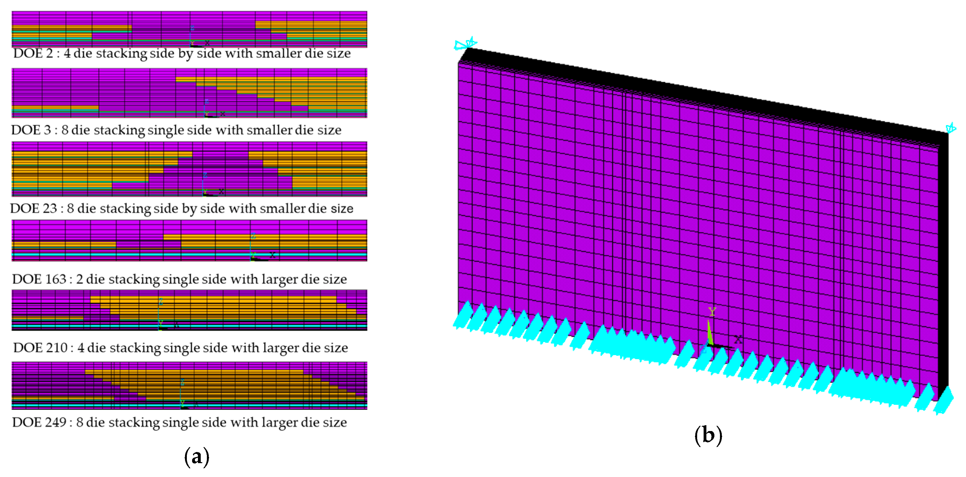
FEA simulation runs were conducted for 250 DOEs to estimate package warpage using ANSYS software (version 2022 R1). In this study, the finite element simulations of package warpage were performed using a higher-order 3D 20-node hexahedral element that supports quadratic displacement behavior and is well-suited for modeling complex geometries with high accuracy. Its capability to handle large deformations, material nonlinearities, and thermal–mechanical coupling makes it particularly appropriate for IC package simulations, where multi-material interactions and thermal gradients significantly influence warpage behavior. The finite element mesh was refined through a mesh sensitivity analysis, and a mesh size of 0.35 mm was selected after a sensitivity study to save solving time without losing accuracy. The TSM reflow process simulation method was used to estimate the warpage behavior of the UFS package with a temperature from 30 °C to 260 °C at the ramp-up stage and 260 °C to 30 °C at the ramp-down stage [12]. This study used a 11 mm × 13 mm UFS package size with a side-by-side and single-side Nand die stack. Instead of the above 10 variable critical factors, some of the fixed parameters, such as ROI size, solder mask height, elastic modulus property, underfill thickness, and location of controller, were considered for FEA model development. Figure 3a shows the 3D model package structure for various DOEs with a side-by-side and single-side Nand die stack (orange color mesh for die stack) considering smaller and larger die widths. Figure 3b shows the 3D half model of a UFS package. In this simulation setup, symmetry and stability constraints were systematically applied to ensure accurate and efficient finite element analysis. A symmetry boundary condition was imposed along the Y = 0 plane by restricting nodal displacement in the Y-direction (UY = 0), effectively modeling only half of the geometry and reducing computational cost. To eliminate rigid body motion, one corner node located at the intersection of the left, top, and bottom surfaces was fully constrained in both the X and Z directions (UX = 0, UZ = 0). Additionally, a second corner node on the opposite side was constrained in the Z direction (UZ = 0) to prevent rotational instability. This combination of constraints ensures structural stability while preserving the model’s ability to deform under applied loads. The package warpage value was calculated for different temperatures using FEA simulation after the 3D model was built for 250 DOEs. Finally, an AI database was created for DL model development after the completion and simulation running of 250 DOEs.

2.3. DNN Regression Model

The DL method is a type of method used to develop a deep learning model with the combination of a DNN algorithm and a huge database required by considering many design parameters from design packages. DNN is a subgroup of the artificial neural network [32] which requires more than one hidden layer and a larger number of neurons to build DNN architecture. As compared to ANN, DNN is more powerful and flexible for different types of datasets and is suitable for a larger number of attributes or input factors. To create the database, a DOE matrix was established, incorporating key factors and leveraging both statistical analysis and FEA simulations. This database was integrated with a DNN algorithm to develop a DL model, which was applied in the present study to reduce development time, enhance prediction accuracy, and enable rapid risk assessment of package warpage.
The DNN regression model was developed by roughly splitting the dataset into 90% training and 10% validation sets, a ratio found to yield optimal performance based on prior experimentation and established machine learning practices [33]. Both subsets were standardized using preprocessing techniques to ensure consistent feature scaling. The DNN architecture was then optimized by tuning the number of neurons and hidden layers, with each node computing outputs via weighted inputs, biases, and activation functions. The model was trained using backpropagation and gradient descent, and its performance was evaluated on the validation set using the coefficient of determination R 2 score and mean absolute percentage error (MAPE). Training was halted once the model achieved an MAPE below 10% and an R 2 score between 0.95 and 0.99, indicating high predictive accuracy. According to this study, if a new design option is selected within the predefined input range, the model can make accurate predictions. However, if the design falls outside this range, additional data must be incorporated to expand the parameter space and retrain the model for improved prediction accuracy.
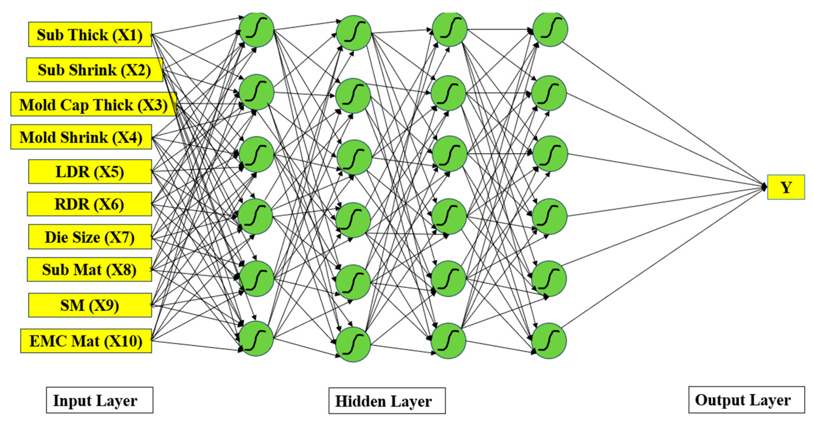
In this study, the architecture of the DNN, including its layered structure and data flow, is illustrated schematically in Figure 4. It has one input layer, four hidden layers, and one output layer, and each layer has six neurons. Since this DNN structure has more than one hidden layer and uses more neurons, it is known as a DL model. Input data is given to the input layer and calculated in the hidden layer with the help of bias, weight, and an activation function. Once the calculation is complete in the hidden layer, the result is displayed in the output layer [32]. The beauty of the DL model is its ability to support both linear and nonlinear datasets, as well as multivariate relationships. Compared to other machine learning algorithms, DL is more flexible to different kinds of datasets, such as smaller or larger datasets. In addition, various activation functions and optimizers can be used to optimize both the training and validation datasets with minimum error to avoid overfitting.
This DL model calculates the output result at each node using an objective function as follows [33]:
z i l = i = 1 n w j i l a i l + b i l
where a i l is the i t h activation element of the l t h layer in the hidden layer. b i l is bias, a i l is equal to the input value times the weight W j i l and rectified logic unit (ReLU) activation function is used for each hidden layer. It is the most extensively utilized activation function for deep learning applications, and it produces cutting-edge outcomes. The ReLU is a high-speed learning activation function that has gained popularity for its exceptional performance in deep learning. It surpasses Sigmoid and Tanh activation functions in terms of both performance and generalization. This is due to its close approximation to a linear function, which retains the simple optimization features of linear models [34]. The ReLU activation function applies a threshold operation to each input element, setting any values less than zero to zero. Thus, the ReLU is given by [34]:
z = max 0 , z = z i             i f   z i 0 0 ,                 i f   < 0
where z is the input value and ( z ) is the ReLU activation function. This DL algorithm helps to build the DL model to predict the package warpage of UFS package. To measure the accuracy of the DL model, we can use the R 2 score error calculation method and the mean absolute percentage error (MAPE) formula, which we have discussed in the previous study [33]. The MAPE equation can be used to determine the percentage error between the actual warpage value and the predicted warpage value, while R 2 score indicates the consistency of the DL model.

3. Results and Discussion

3.1. FEA Simulation Warpage Result

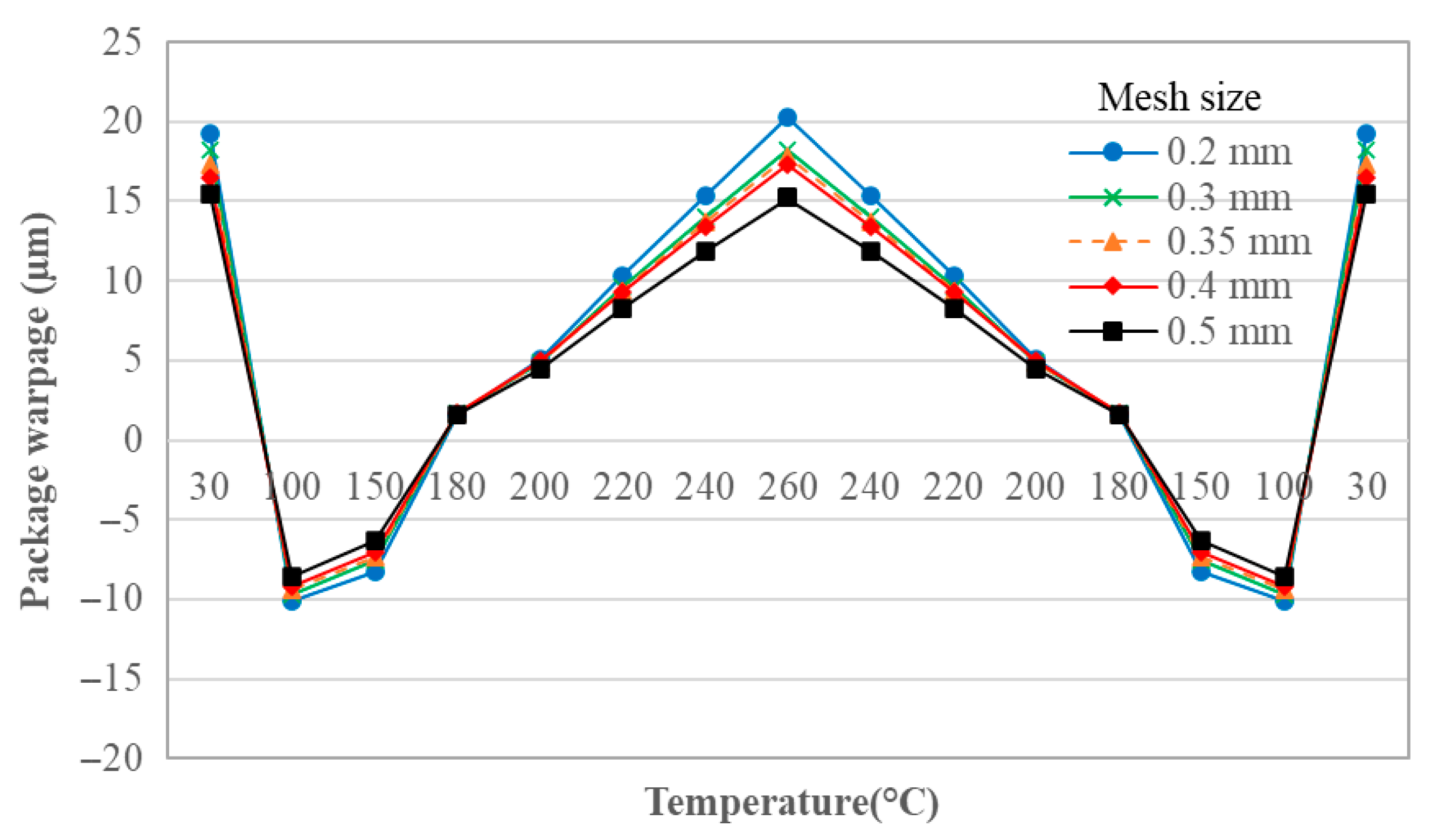
The FEA simulation was employed to evaluate the warpage behavior of UFS package structures under varying thermal conditions. In this study, a positive warpage refers to the convex shape of the warped package with the solder balls facing down while a negative warpage refers to a concave shape. Figure 5 illustrates the warpage behavior of an 8-die side-by-side package structure across various temperatures, evaluated using different mesh sizes ranging from 0.2 mm to 0.5 mm. The results indicate that the variation in mesh size has a negligible effect on the warpage simulation results. Based on this sensitivity study, a warpage converged with a criterion of 2 µm, a mesh size of 0.35 mm, and was determined in FEA models for plan element size. This resolution was found to be sufficient to accurately capture the warpage behavior while maintaining computational efficiency, particularly for large-scale simulations involving 250 DOE runs.
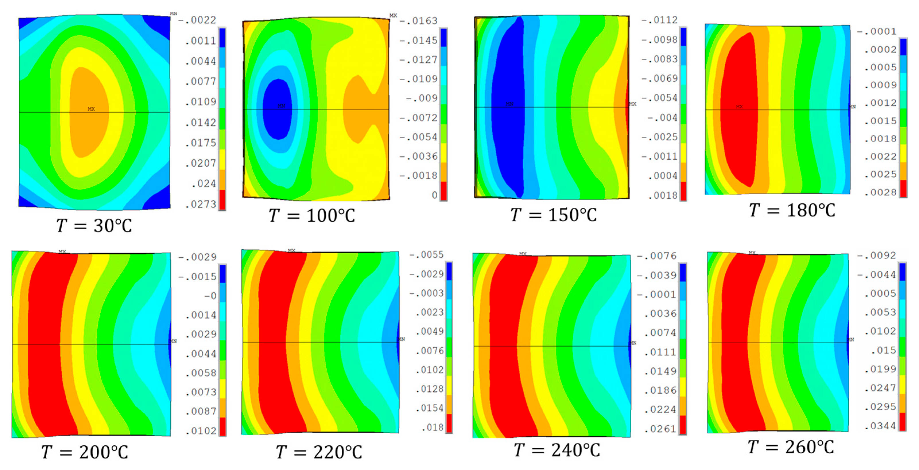
Figure 6 illustrates the thermal-induced warpage captured through FEA simulations, with contour plots spanning temperatures from 30 °C to 260 °C. The warpage magnitude is represented by a color gradient, where blue denotes minimal and red indicates maximal out-of-plane deformation. The results demonstrate a progressive increase in warpage with increasing temperature from 180 °C up to 260 °C. Localized high-deformation regions suggest CTE mismatches among package layers. These findings inform material selection, layer stack configuration, and thermal-mechanical design strategies to enhance reliability and manufacturability. Significant differences in warpage behavior were observed across UFS package variants, attributed to variations in material properties and structural design. To support data-driven design, this study contributed to the development of an AI-ready database, comprising 250 simulation-derived entries capturing warpage characteristics across design and thermal parameters.

3.2. DNN Trained Model and Validation

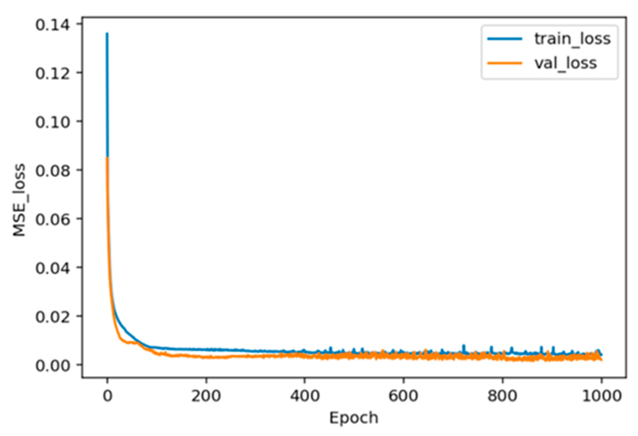
The AI database was generated using FEA simulation techniques to develop a DNN regression model. After conducting the warpage simulations, 234 datasets were chosen for training, and 16 datasets were selected for validation. This study utilized DNN model parameters implemented through the Python (version 3.11) programming language and DNN algorithm, as detailed in the methodology chapter, to construct the DNN model. Table 2 illustrates the DNN model parameters. Before the construction of the DNN model, the training and validation datasets were subjected to normalization using both min-max scaling and standardization techniques to ensure consistent feature scaling. The Min-Max Scaler moves the data so that all critical features are exactly between 0 and 1, as listed in Table 3. This signifies that all the data in a two-dimensional dataset is contained within the rectangle formed by the x-axis between 0 and 1 and the y-axis between 0 and 1. After trying a few combinations between the neuron and hidden layer for proper optimization, six neuron numbers and four hidden layers were selected to construct the DNN architecture as shown in Figure 4. These parameters are selected based on the dataset used for training the model. The activation function is ReLU for output calculation at each node, and the mean square error (MSE) loss function is used to calculate the error between the FEA simulation warpage and the DNN predicted warpage. A learning rate of 0.0001 is set for the smooth running of the DNN model and to avoid overfitting issues. The number of epochs (iteration) was selected at 500 or 1000 for minimizing the errors between training and validation warpage results, as shown in Figure 7. Both training and validation MSE losses were very close, and this can avoid overfitting issues of the DNN model.
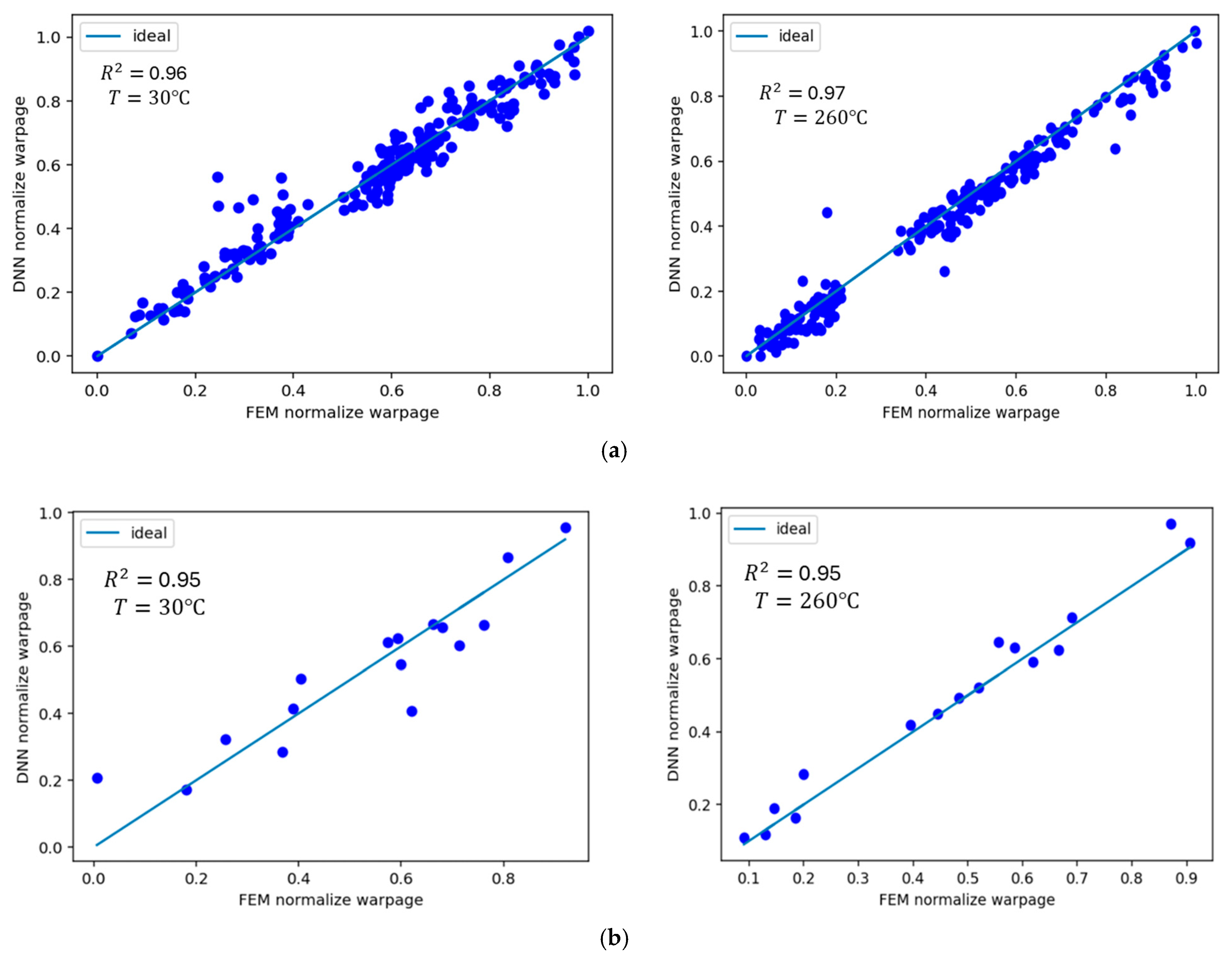
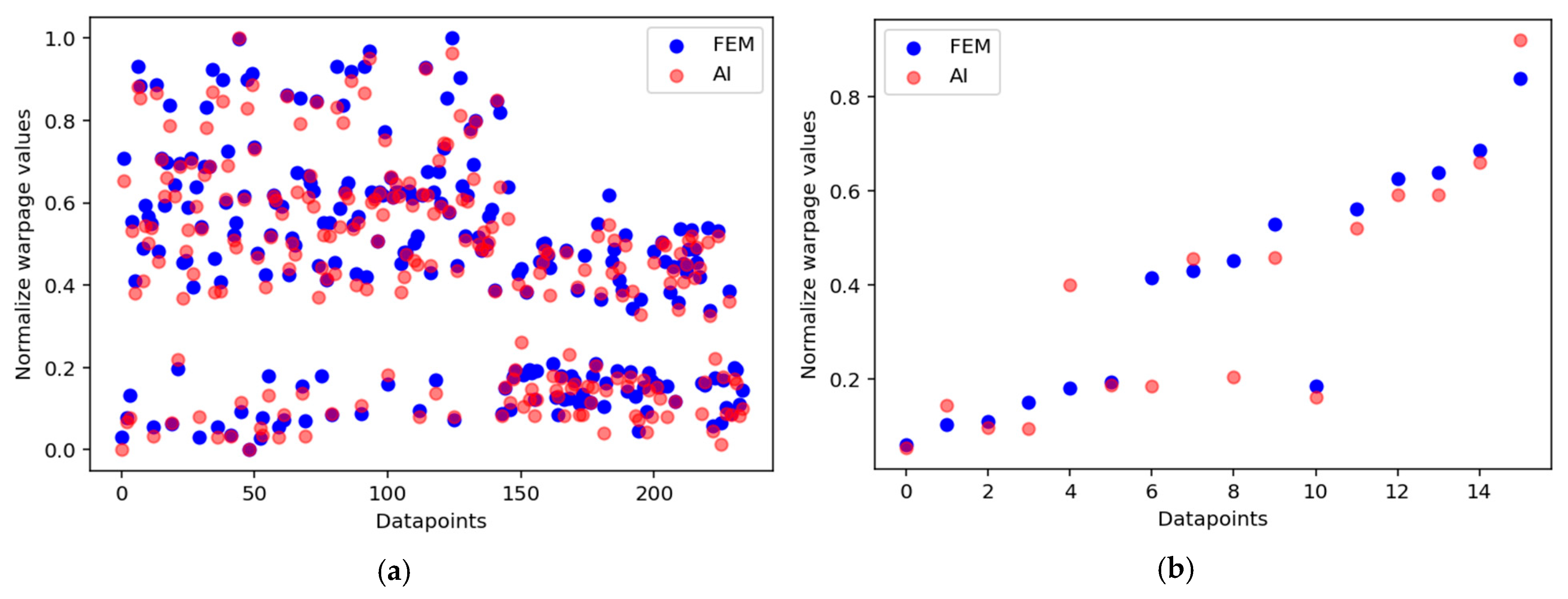
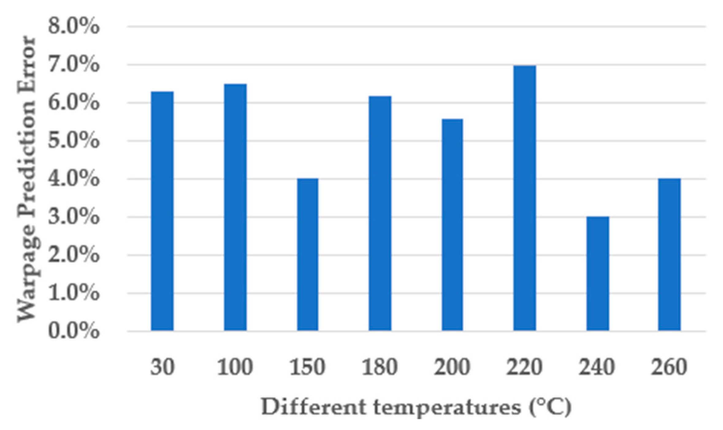
Figure 8a shows the DNN training model accuracy with 30 °C and 260 °C temperatures for the warpage dataset. Table 4 lists the   R 2 score range as 0.97~0.99 for various temperatures, which indicates the accuracy of the DNN regression model. Figure 8b shows the validated DNN regression model with a R 2 score value (0.95~0.97) for different temperatures due to the usage of the K-Fold cross-validation method [34]. This K-Fold cross-validation method can also try to reduce overfitting and DNN model complexity. Figure 9a,b show the similarity between actual and predicted warpage data points for 234 training datasets and 16 validated datasets. This represents a better performance for the DNN model. Eventually, this study will discuss error analysis for predicted warpage with various temperatures ranging from 30 °C to 260 °C for eight temperature points. Figure 10 represents the warpage prediction MAPE vs. the 250 warpage datasets at different temperature conditions. The MAPE between the FEA simulation and DNN prediction warpage is less than 7% for the warpage dataset at various temperatures. This study has confirmed that the DNN model shows better accuracy for package warpage prediction, and this DL model can be used to do a quick risk assessment of package warpage for a new design package.

3.3. Factor Sensitivity Study Using Regression Model

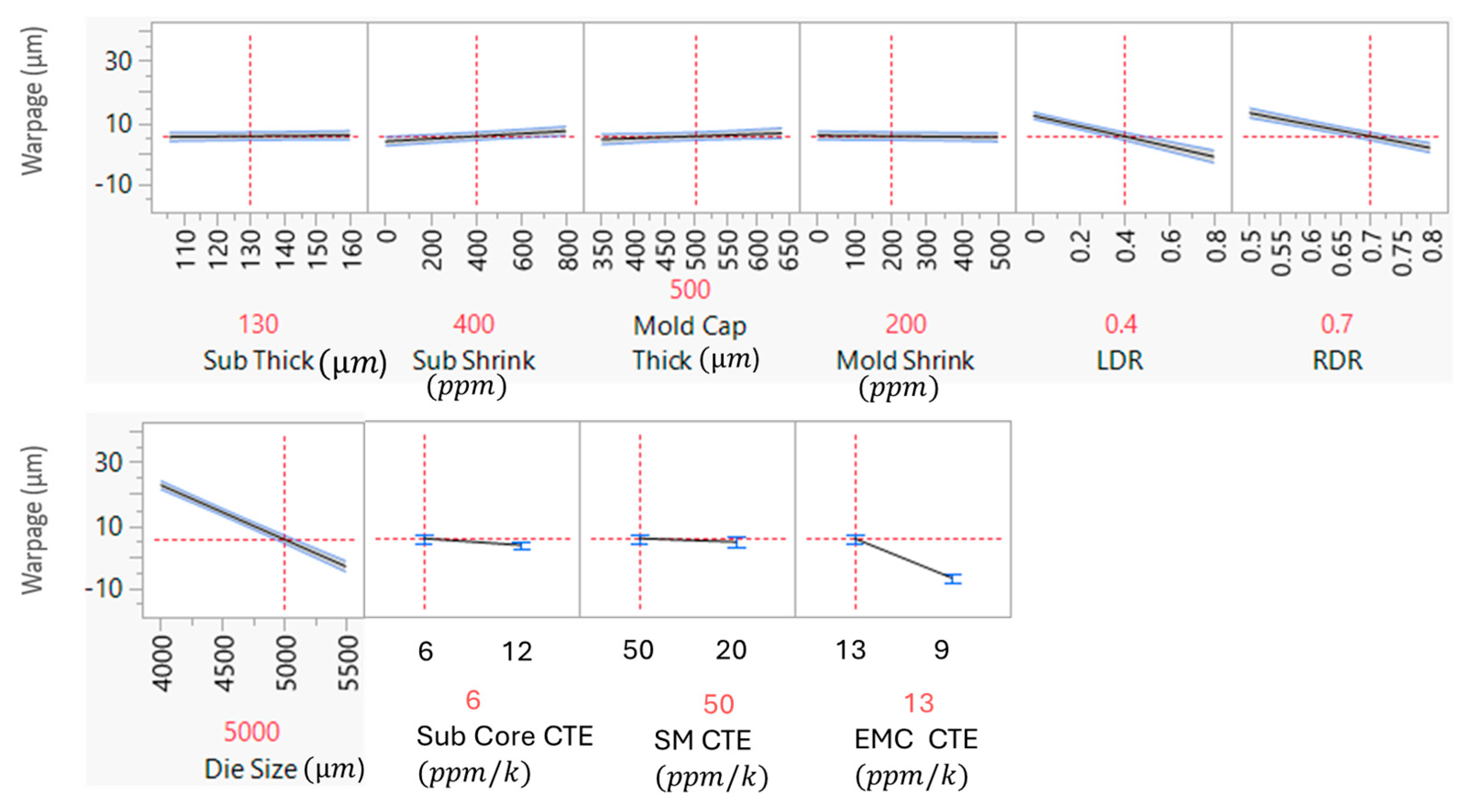
A regression model is used to perform the factor sensitivity analysis of the UFS package. This regression model is significantly faster than the traditional FEA simulation method for sensitivity analysis because FEA simulation can perform sensitivity analysis one factor at a time. However, the ML regression model can carry out a sensitivity analysis for all ten factors at a time. Therefore, this regression model can save a significant amount of design cycle time. Figure 11 shows the factor sensitivity study of ten critical factors used in the DNN regression model at reflow temperature. Sensitive factors include die size, EMC material CTE, die stacking ratios, mold cap thickness, and substrate material CTE. However, substrate thickness, mold shrinkage, and substrate shrinkage are less significant factors on warpage of the UFS package. To decrease UFS package warpage, the recommendation is to use a larger die size, lower EMC CTE, thinner die stacking, thicker substrate, and thicker mold cap. As illustrated in Figure 11, the values highlighted in red for each factor were referenced for this sensitivity analysis.

3.4. DNN Regression Model Application on New Package Design

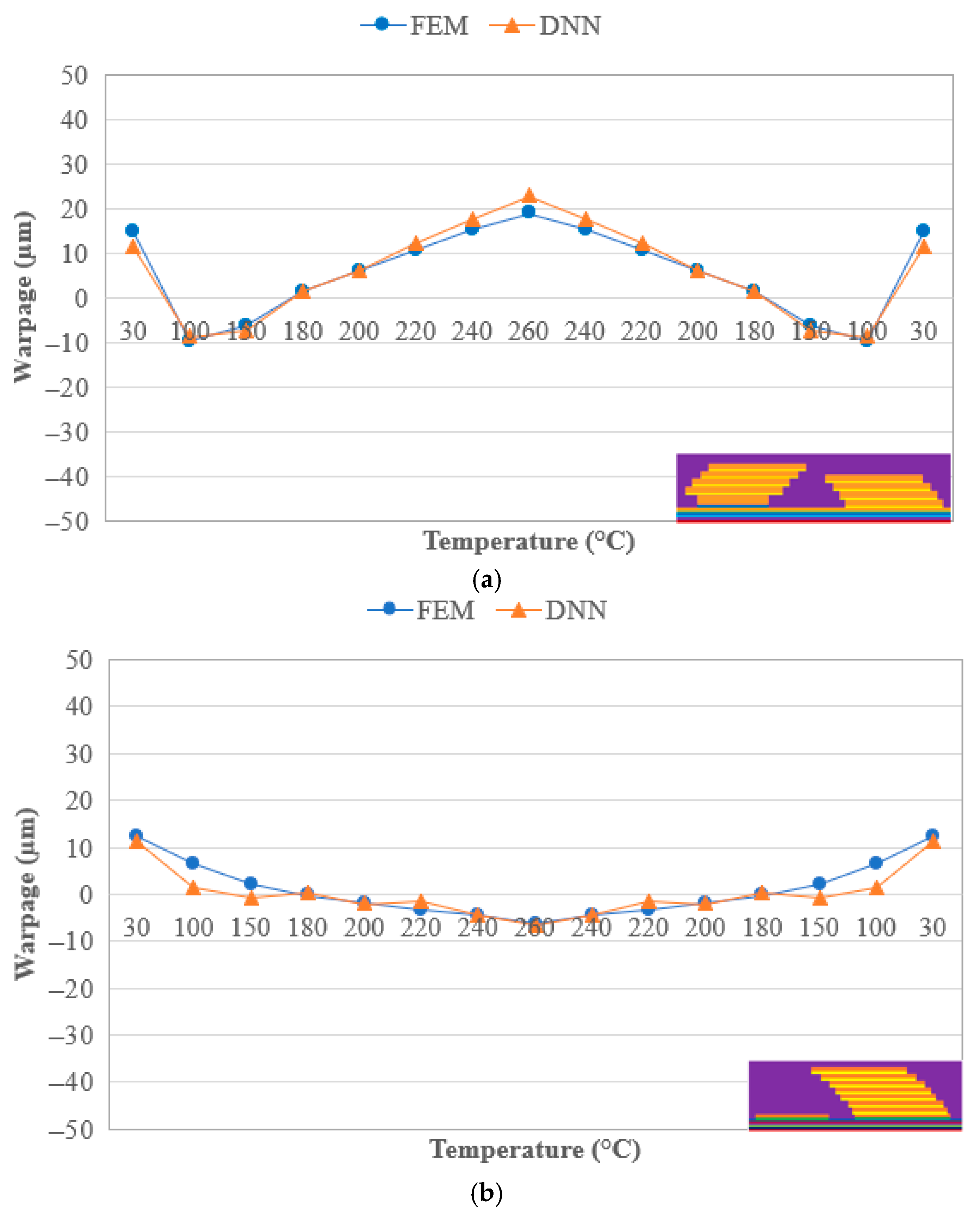
The main purpose of this study is to support package warpage assessment for NPI requests in a timely manner. This DNN regression model can reduce the solving time instead of using the FEA simulation. Here, this study has selected a few NPI cases for risk assessment with different die stacking options using a DNN model. Figure 12a shows the warpage comparison between the FEA simulation and the DNN model prediction with various temperatures. FEA simulation and AI/DL prediction both exhibit similar warpage behavior at all temperatures. Accordingly, there is good agreement between simulation and AI/DL prediction. This warpage result is based on side-by-side 8-die stacking with a smaller die size. Similarly, Figure 12b also shows good agreement between the FEA simulation and DNN prediction warpage result for single-sided 8-die stacking with a larger die size. However, the cycle time required for FEA simulation is few days for each design option, whereas the AI/DL prediction method requires only 30 min to build the model and predict the package warpage. For the above four options, the cycle time has been reduced from a few days to 30 min. Therefore, the package warpage optimization becomes feasible, because warpage prediction of any design parameter combination of an advanced package can be completed in a few minutes.
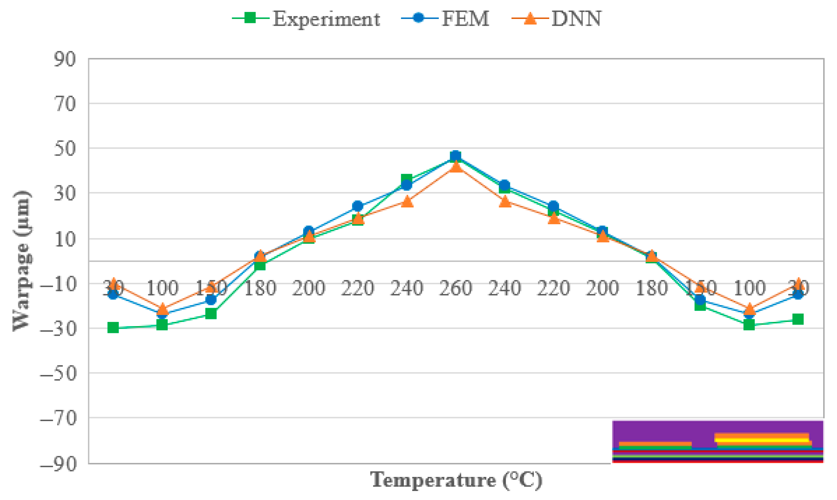
In the end, the predicted TSM warpage of the experiment, FEA simulation, and DNN model result for our UFS package structure are compared. Here, the DNN-predicted warpage is the same as the FEA simulation result and very close to the experiment result as shown in Figure 13. However, the AI technique may require 30 min to build the model and predict output, the simulation technique will take few days, and the experiment will require more than one month to obtain the package warpage of the UFS package structure. Therefore, industry product design and development should leverage AI/DL to optimize structure and performance, improve cost-effectiveness, and shorten development time.

4. Conclusions

This study has successfully established an AI-based DNN model using datasets from FEA simulation technology to predict package warpage of the UFS memory package. This study has also successfully validated FEA simulation results with experimental data of UFS package. FEA simulation is used to generate warpage data to build the DNN model and predict the package warpage by considering the geometry parameters and materials of the UFS package. The developed DNN model can be used to assess package warpage and optimization for NPI design requests effectively and efficiently with good accuracy. The cycle time on package warpage assessment is drastically reduced by DNN model. Key findings are summarized below:
  • Ten critical factors relating to geometry and materials have been defined based on experience and sensitivity study to develop DNN model for predicting package warpage on UFS memory package.
  • To reduce package warpage, wider die size, lower die stacking ratios, lower EMC CTE, thinner die stacking, thicker substrate, and thicker mold cap are recommended based on DNN model prediction on UFS package warpage.
  • The implementation of a deep learning model in NPI support significantly reduces cycle time. Compared to traditional methods such as FEA simulation, the AI-based approach achieves approximately 95% reduction in development time and effectively supports for package optimization on UFS package.
  • In general, package design and development should leverage AI to optimize structure/performance, reduce costs, and shorten development time. This physics-based DNN model can also be applied to other processes and reliability-related risk assessment areas such as strip warpage, solder joint reliability, thermal analysis, and package strength for advanced packages, which are our on-going and future work.

Author Contributions

Conceptualization, S.K.P., F.X.C. and Y.C.O.; methodology, S.K.P. and F.X.C.; software, S.K.P.; validation, S.K.P. and F.X.C.; formal analysis, S.K.P. and F.X.C.; investigation, S.K.P. and F.X.C.; resources, S.K.P., F.X.C., H.W.N. and Y.C.O.; data curation, S.K.P. and F.X.C.; writing—original draft preparation, S.K.P.; writing—review and editing, F.X.C. and Y.C.O.; visualization, S.K.P.; supervision, F.X.C., Y.C.O., H.W.N. and G.K.; project administration, F.X.C. and Y.C.O. All authors have read and agreed to the published version of the manuscript.

Funding

This research received no external funding.

Conflicts of Interest

Sunil Kumar Panigrahy was employed by the company Micron Technology Operations India LLP. Fa Xing Che, Yeow Chon Ong, and Hong Wan Ng were employed by the company Micron Semiconductor Asia Operations Pte. Ltd. and Gokul Kumar was employed by the company Micron Technology, Inc. The remaining authors declare that the research was conducted in the absence of any commercial or financial relationships that could be construed as a potential conflict of interest.

References

  1. Su, M.; Cao, L.; Lin, T. Warpage Simulation and Experimental Verification for 320 mm × 320 mm Panel Level Fan-Out Packaging Based on Die-First Process. Microelectron. Reliab. 2018, 83, 29–38. [Google Scholar] [CrossRef]
  2. Onn, S.J.; Tan, K.S.; Tau, T.Y.; Yap, S.S.; Lau, C.S.; Chin, Y.T. Warpage studies of printed circuit boards with Shadow Moir and simulations. In Proceedings of the IEEE 38th International Electronics Manufacturing Technology Conference, Melaka, Malaysia, 4–6 September 2018; pp. 1–5. [Google Scholar]
  3. Nam, S.; Kang, J.; Lee, I.; Kim, Y.; Yu, H.J.; Kim, D.W. Investigation on Package Warpage and Reliability of the Large Size 2.5D Molded Interposer on Substrate (MIoS) Package. In Proceedings of the 2022 IEEE 72nd Electronic Components and Technology Conference (ECTC), San Diego, CA, USA, 31 May–3 June 2022; pp. 643–647. [Google Scholar]
  4. Wang, D.W.; Huang, H.M.; HO, S.C.; Liu, A.H.; Liu, D.S. Study of warpage characteristics of molded stacked-die MCP using Shadow Moiré and Micro Moiré techniques. In Proceedings of the 60th Electronic Components and Technology Conference (ECTC), Las Vegas, NV, USA, 27–30 May 2010; pp. 1968–1973. [Google Scholar]
  5. Geng, M.; Zhang, Y.; Li, X.; Wang, J.; Liu, H. Study on Package Warpage Based on Three-Dimensional Flow Simulation. In Proceedings of the 23rd International Conference on Electronic Packaging Technology (ICEPT), Dalian, China, 10–13 August 2022; pp. 1–4. [Google Scholar]
  6. Praful, P.; Bailey, C. Warpage in Wafer-Level Packaging: A Review of Causes, Modelling, and Mitigation Strategies. Front. Electron. 2025, 5, 1515860. [Google Scholar] [CrossRef]
  7. Baek, J.W.; Yang, W.S.; Hur, M.J.; Yun, J.C.; Park, S.J. Representative Volume Element Analysis for Wafer-Level Warpage Using Finite Element Methods. Mater. Sci. Semicond. Process. 2019, 91, 392–398. [Google Scholar] [CrossRef]
  8. Chen, C.; Yu, D.Q.; Wang, T.; Xiao, Z.Y.; Wan, L.X. Warpage Prediction and Optimization for Embedded Silicon Fan-Out Wafer-Level Packaging Based on an Extended Theoretical Model. IEEE Trans. Compon. Packag. Manuf. Technol. 2019, 9, 845–853. [Google Scholar] [CrossRef]
  9. Wang, S.; Sun, Y.; Sheng, C.; Feng, Z.; Li, R.; Xue, L.; Liu, J.; Liu, S. Warpage Analysis and Prediction of the Advanced Fan-Out Technology Based on Process Mechanics. IEEE Trans. Compon. Packag. Manuf. Technol. 2021, 11, 2201–2213. [Google Scholar] [CrossRef]
  10. Tsai, C.H.; Liu, S.W.; Chiang, K.N. Warpage Analysis of Fan-Out Panel-Level Packaging Using Equivalent CTE. IEEE Trans. Device Mater. Reliab. 2020, 20, 51–57. [Google Scholar] [CrossRef]
  11. McCann, S.; Lee, H.H.; Refai-Ahmed, G.; Lee, T.; Ramalingam, S. Warpage and Reliability Challenges for Stacked Silicon Interconnect Technology in Large Packages. In Proceedings of the IEEE 68th Electronic Components and Technology Conference (ECTC), San Diego, CA, USA, 29 May–1 June 2018; pp. 2345–2350. [Google Scholar]
  12. Yu, W.; Yang, P.S.Y.; Glancey, C.; Ong, Y.C.; Ng, H.W. Package Warpage Modeling by Considering Shrinkage Behavior of EMC and Substrate. In Proceedings of the 23rd Electronics Packaging Technology Conference, Singapore, 1–3 December 2021; pp. 547–552. [Google Scholar]
  13. Panigrahy, S.K.; Tseng, Y.C.; Lai, B.R.; Chiang, K.N. An overview of AI-Assisted design-on-Simulation technology for reliability life prediction of advanced packaging. Materials 2021, 14, 5342. [Google Scholar] [CrossRef] [PubMed]
  14. Liu, S.W.; Panigrahy, S.K.; Chiang, K.N. Prediction of Fan-Out Panel Level Warpage using Neural Network Model with edge Detection Enhancement. In Proceedings of the IEEE 70th ECTC Conference, Virtual, 3–30 June 2020; pp. 1626–1631. [Google Scholar]
  15. Che, F.X.; Ong, Y.C.; Ng, H.W.; Pan, L.; Shina, K.; Glancey, C.; Kumar, G. Physics-driven Regression Algorithm on Solder Joint Fatigue Life Prediction for Mobile SiP Packages. In Proceedings of the 73rd Electronic Components and Technology Conference, Orlando, FL, USA, 30 May–2 June 2023; pp. 420–425. [Google Scholar]
  16. Panigrahy, S.K.; Chiang, K.N. Study on an Artificial Intelligence Based Kernel Ridge Regression Algorithm for Wafer Level Package Reliability Prediction. In Proceedings of the IEEE 71st Electronic Components and Technology Conference (ECTC), San Diego, CA, USA, 1 June–4 July 2021; pp. 1435–1441. [Google Scholar]
  17. Chen, C.Y.; Wang, W.C.; Chang, K.S.; Chen, T.Y.; Chen, D.L.; Lin, Y.C. Development of Artificial Neural Network and Topology Reconstruction Schemes for Fan-Out Wafer Warpage Analysis. In Proceedings of the 2021 IEEE 71st Electronic Components and Technology Conference (ECTC), San Diego, CA, USA, 1–4 June 2021; pp. 1450–1456. [Google Scholar]
  18. Gupta, S.; Al-Obaidi, S.; Ferrara, L. Meta-Analysis and Machine Learning Models to Optimize the Efficiency of Self-Healing Capacity of Cementitious Material. Materials 2021, 14, 4437. [Google Scholar] [CrossRef] [PubMed]
  19. Sun, J.; Sun, M.; Guo, H.; Yan, P.; Ji, J.; Xu, L. Research on Edge Surface Warping Defect Diagnosis Based on Fusion Dimension Reduction Layer DBN and Contribution Plot Method. J. Mech. 2020, 36, 889–899. [Google Scholar] [CrossRef]
  20. Kuschmitz, S.; Ring, T.P.; Watschke, H.; Langer, S.C.; Vietor, T. Design and Additive Manufacturing of Porous Sound Absorbers—A Machine-Learning Approach. Materials 2021, 14, 1747. [Google Scholar] [CrossRef] [PubMed]
  21. Song, H.; Ahmad, A.; Ostrowski, K.A.; Dudek, M. Analyzing the Compressive Strength of Ceramic Waste-Based Concrete Using Experiment and Artificial Neural Network (ANN) Approach. Materials 2021, 14, 4518. [Google Scholar] [CrossRef]
  22. Farooq, F.; Czarnecki, S.; Niewiadomski, P.; Aslam, F.; Alabduljabbar, H.; Ostrowski, K.A.; Sliwa-Wieczorek, K.; Nowobilski, T.; Malazdrewicz, S. A Comparative Study for the Prediction of the Compressive Strength of Self-Compacting Concrete Modified with Fly Ash. Materials 2021, 14, 4934. [Google Scholar] [CrossRef] [PubMed]
  23. Huang, X.; Wasouf, M.; Sresakoolchai, J.; Kaewunruen, S. Prediction of Healing Performance of Autogenous Healing Concrete Using Machine Learning. Materials 2021, 14, 4068. [Google Scholar] [CrossRef] [PubMed]
  24. Salazar, A.; Xiao, F. Design of Hybrid Reconstruction Scheme for Compressible Flow Using Data-Driven Methods. J. Mech. 2020, 36, 675–689. [Google Scholar] [CrossRef]
  25. Song, S.-H. A Comparison Study of Constitutive Equation, Neural Networks, and Support Vector Regression for Modeling Hot Deformation of 316L Stainless Steel. Materials 2020, 13, 3766. [Google Scholar] [CrossRef] [PubMed]
  26. Papacharalampopoulos, A.; Michail, C.K.; Stavropoulos, P. Manufacturing Resilience and Agility through Processes Digital Twin: Design and Testing Applied in the LPBF Case. Procedia CIRP 2021, 103, 164–169. [Google Scholar] [CrossRef]
  27. Zhang, Q.; Zhong, C.; Rong, S. Study on Warpage of Flip Chip Structure Based on Finite Element Analysis and Machine Learning Algorithm. In Proceedings of the 25th International Conference on Electronic Packaging Technology (ICEPT), Shenzhen, China, 7–9 August 2024; pp. 1–6. [Google Scholar]
  28. Yao, P.; Yang, J.; Zhang, Y.; Fan, X.; Chen, H.; Yang, J.; Wu, J. Physics-Based Nested-ANN Approach for Fan-Out Wafer-Level Package Reliability Prediction. In Proceedings of the 72nd Electronic Components and Technology Conference (ECTC), San Diego, CA, USA, 31 May 2022; pp. 1827–1833. [Google Scholar]
  29. Lin, Y.C.; Chen, T.Y.; Wang, C.C.; Hung, C.P.; Shou, I.A.; Wang, H.K. GA-NN and Explainable AI for IC Packaging Warpage Optimization: A Case Study on Product Feature. In Proceedings of the 2025 IEEE 75th Electronic Components and Technology Conference (ECTC), Denver, CO, USA, 27–30 May 2025; pp. 1609–1614. [Google Scholar]
  30. Che, F.X.; Ong, Y.C.; Ng, H.W.; Glancey, C.; Kumar, G. Investigation on memory package crack and prevention under temperature cycling test. Mater. Sci. Semicond. Process. 2024, 180, 108560. [Google Scholar] [CrossRef]
  31. Huang, S.; Ji, Z.; Liu, Y.; Ye, N.; Takiar, H. Parametric Optimization and Yield Probability Prediction of Package Warpage. In Proceedings of the IEEE 68th Electronic Components and Technology Conference (ECTC), San Diego, CA, USA, 29 May–1 June 2018; pp. 243–248. [Google Scholar]
  32. McCulloch, W.S.; Pitts, W. A logical calculus of the ideas immanent in nervous activity. Bull. Math. Biophys. 1943, 5, 115–133. [Google Scholar] [CrossRef]
  33. Panigrahy, S.K.; Che, F.X.; Ong, Y.C.; Nune, P.N.; Ng, H.W. Integration of Artificial Neural Network and Finite Element Simulation for Package Warpage Prediction. In Proceedings of the IEEE 25th Electronics Packaging Technology Conference (EPTC), Singapore, 5–8 December 2023; pp. 926–931. [Google Scholar]
  34. Nwankpa, C.; Ijomah, W.; Gachagan, A.; Marshall, S. Activation functions: Comparison of trends in practice and research for deep learning. arXiv 2018, arXiv:1811.03378. [Google Scholar] [CrossRef]
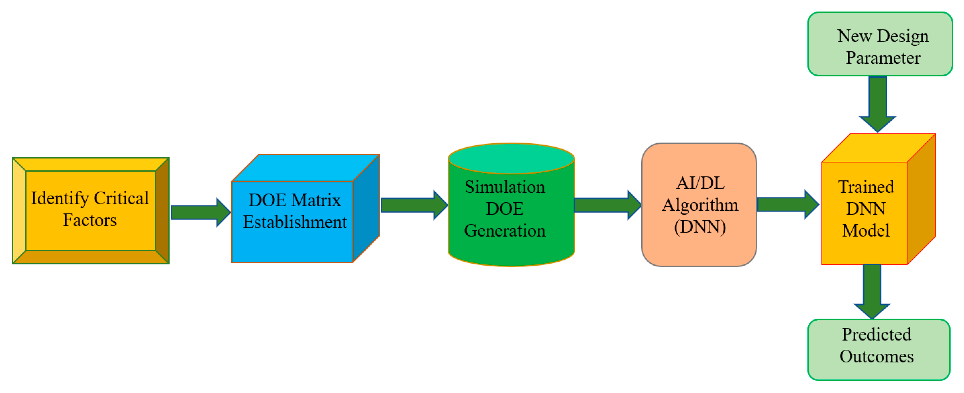
Figure 1. Deep learning model flow process for risk assessment.
Chips 04 00035 g001
Figure 2. Schematic diagram of different UFS packages: (a) side-by-side die stacking with smaller die size; (b) single-side die stacking with larger die size.
Chips 04 00035 g002
Figure 3. FEA 3D half model for different packages: (a) different die stacking package structures for various DOE numbers with smaller and larger die width sizes; (b) FEA model of package size.
Chips 04 00035 g003
Figure 4. Schematic diagram of DNN architecture.
Chips 04 00035 g004
Figure 5. Mesh sensitivity study on temperature-dependent package warpage.
Chips 04 00035 g005
Figure 6. Temperature-dependent package warpage for package with 8 dies stacked at different temperatures (unit: mm).
Chips 04 00035 g006
Figure 7. Schematic diagram of MSE loss vs. epoch numbers of DNN model (example for 260 °C warpage).
Chips 04 00035 g007
Figure 8. DNN training model accuracy and validation at various temperatures: (a) training model; (b) model validation.
Chips 04 00035 g008
Figure 9. Scatter plot of warpage similarity between FEA and AI value: (a) 234 trained data; (b) 16 validation data.
Chips 04 00035 g009
Figure 10. Warpage prediction MAPE of 250 warpage datasets at various temperatures.
Chips 04 00035 g010
Figure 11. Effect of factors on UFS package warpage.
Chips 04 00035 g011
Figure 12. FEA simulation warpage vs. DNN-predicted warpage: (a) Side-by-side stack with smaller die; (b) Single stack with larger die package.
Chips 04 00035 g012
Figure 13. Package warpage comparison among experiment, FEA simulation, and DNN prediction.
Chips 04 00035 g013
Table 1. Various levels of 10 critical factors.
No of FactorsFactors NameLevel
X1Substrate Thickness (µm)106, 127, 160
X2Substrate Shrinkage (ppm)0, 400, 800
X3Mold Cap Thickness (µm)350, 500, 640
X4EMC Shrinkage (ppm)0, 250, 500
X5LDR (Left Side Die Stack Ratio)0, 0.5, 0.8
X6RDR (Right Side Die Stack Ratio)0.5, 0.65, 0.8
X7Die Width (µm)4000, 5500
X8Substrate Material CTE (ppm/k)6, 12
X9Solder Mask CTE (ppm/k)20, 50
X10EMC Material CTE (ppm/k)9, 13
Table 2. DNN model parameter.
Neural Network ParameterAttribute Range SettingFinal Attribute/Value
Neuron Number1~106
Hidden Layer2~64
Activation FunctionSigmoid, Relu, Tanh, SoftMaxRelu
Loss FunctionMSEMSE
Learning Rate0~10.0001
Batch Size2~102
Epoch (Iteration)100~2000500, 1000
PreprocessMin-Max, Robust, StandardMin-Max, Standard Scaler
Cross-Validation (K-Fold)5, 10, 1515
Training/Validation234/16234/16
Table 3. Normalized datasets with values between 0 to 1.
FactorsX1X2X3X4X5X6X7X8X9X10
DOE 10100.50.6250.50000
DOE 200.500011101
DOE 30.388000.5011100
DOE 40.3880.501001000
DOE 50110110110
DOE 6010.5170.500.51100
DOE 71010.500.51001
DOE 8100.517100.51101
DOE 9110.5170011101
DOE 1010.500.5001001
Table 4. DNN training and validation accuracy at various temperatures.
Temperature °C Training R 2 ScoreValidation R 2 Score
300.950.95
1000.970.97
1500.990.96
1800.990.96
2000.990.96
2200.990.97
2400.980.97
2600.970.95
Disclaimer/Publisher’s Note: The statements, opinions and data contained in all publications are solely those of the individual author(s) and contributor(s) and not of MDPI and/or the editor(s). MDPI and/or the editor(s) disclaim responsibility for any injury to people or property resulting from any ideas, methods, instructions or products referred to in the content.