Radiation-Induced Effects on Semiconductor Devices: A Brief Review on Single-Event Effects, Their Dynamics, and Reliability Impacts


Abstract
1. Introduction
2. Cumulative Effects: Total Ionizing Dose (TID) and Displacement Damage (DD)
3. Single-Event Effects
3.1. General Aspects and Test Methods
- Large beam spot to cover the entire area of interest or a microbeam with scanning capability. In the case of a large spot, it should be at least 90% uniform in the considered area.
- Flux: The particle flux should fall within the range of to ions.cm−2.s−1. This requirement ensures that the device is not hit by more than one ion during a data acquisition cycle.
- Range: The minimum beam penetration should be 30 µm in silicon. However, for several studies, it can be assumed that the range should simply be much greater than the thickness of the active layer [38].
- Energy and LET: The energy and linear energy transfer (LET) (linear energy transfer is the amount of energy deposited in the device per unit path length) of the beam in the device must be known within a maximum variation of 10%. The LET depends on the particle energy and species and is generally calculated through computational simulations, using SRIM software [42], for example. To ensure that the LET does not vary by more than 10%, it must be guaranteed that the Bragg curve in the region where the charge is collected (the active layer) forms a plateau, a condition that is usually met when the range is much greater than the thickness of the active layer.
- Beams: Tests should be performed with several beams, ideally some with the same LET, as the effects can vary with the ion species. If possible, data should be obtained up to twice the saturation LET.
- Single-Event Transient—SET: A transient effect (voltage/current pulses) that propagates through the circuit and can trigger subsequent effects. Its correction is complex, as the transient effect generated in the device may only be detected at another point in the circuit. Newer technologies are more susceptible to SET because the critical charge is smaller.
- Single-Event Upset—SEU: The generation of charge produces current/voltage spikes (SET) that affect the logic (on/off) of the device. In general, these effects can be summarized as a bit flipping from 0 to 1 or vice versa. These effects primarily affect digital devices. In cases where multiple bits are affected, this effect is called Multiple-Bit Upset (MBU) [48];
- Single-Event Functional Interrupt—SEFI: A subclass of SEU related to high-density digital devices such as Field-Programmable Gate Arrays (FPGAs), as radiation can affect the logical system of the component.
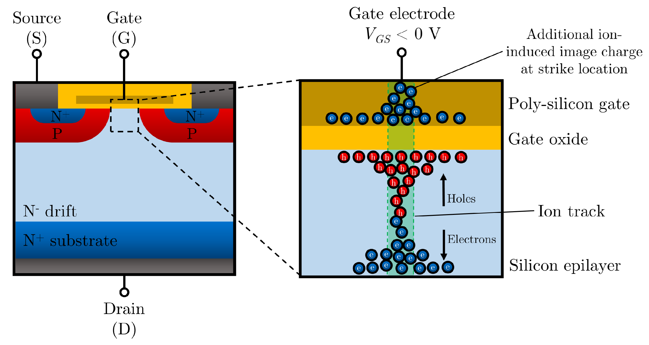
- Single-Event Latch-Up—SEL: A parasitic thyristor is activated in CMOS circuits by a high-LET particle, generating a high current flow and overheating, potentially destroying the device. Since the parasitic thyristor is activated in deep layers (below the source and drain channels), it is important that the particle deposits energy in this region.
- Single-Event Burnout—SEB: Power devices in the “off” state can be activated by a particle capable of generating enough charge to burn out the device.
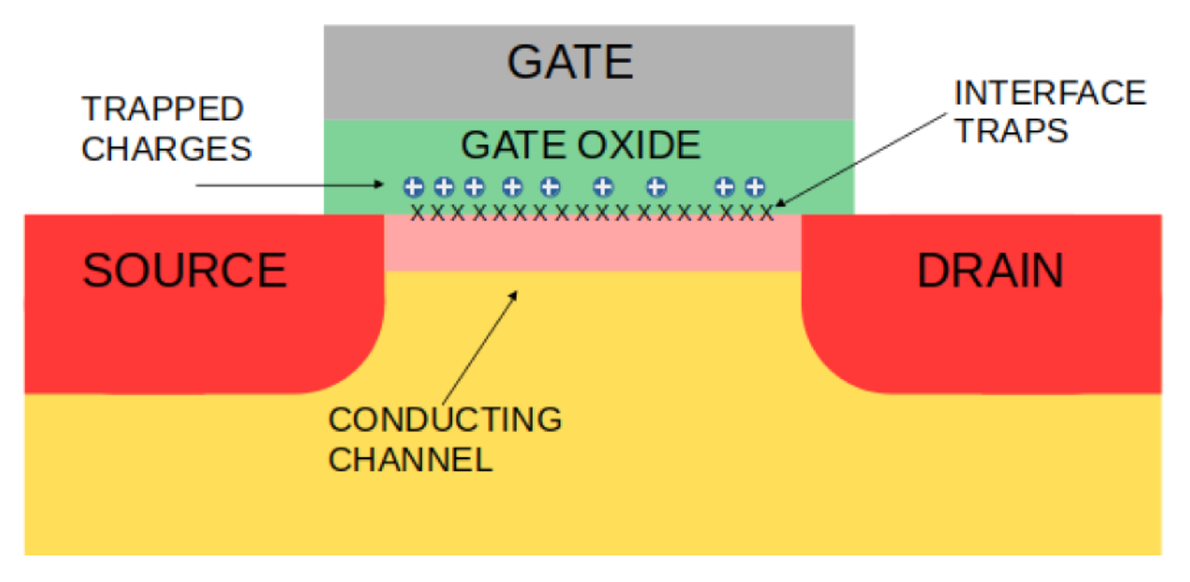
- Single-Event Gate Rupture—SEGR: Primarily affects MOS power devices. The accumulation of charges at the Si/SiO2 interface increases the electric field in the gate oxide, permanently breaking its dielectric strength.
3.2. Cross-Section and Failure Rate
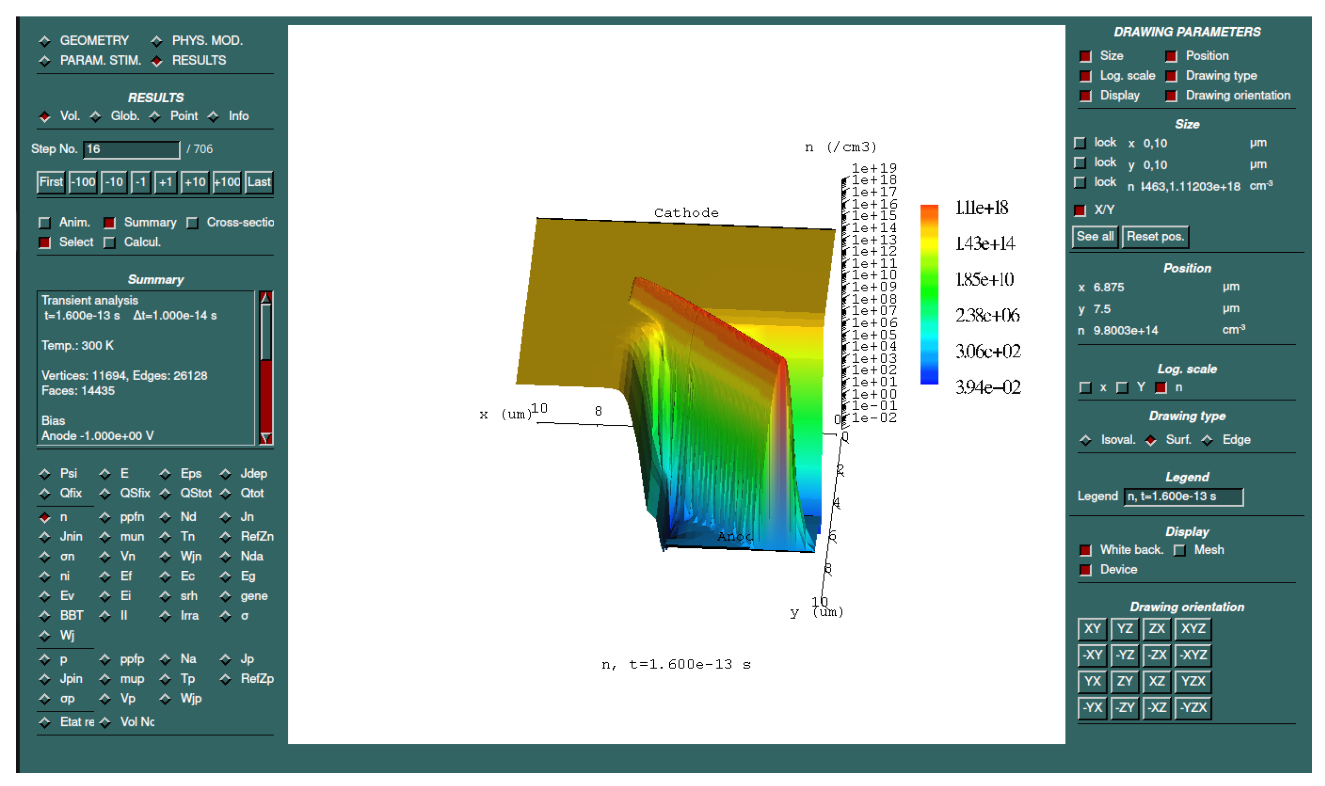
3.3. Single-Event-Transients: Charge Injection and Collection
- .
- High-energy ions (>8.0 MeV/u) in large tech node devices: LET can be considered constant and equal to the value at the surface;
- High-energy ions (>8.0 MeV/u) in small tech node devices: radial LET variation should be considered;
- Low-energy ions (<0.3 MeV/u) in large tech node devices: longitudinal LET variation should be considered;
- Low-energy ions (<0.3 MeV/u) in small tech node devices: both longitudinal and radial LET variations should be considered.
3.4. Simulations and Computational Methods
3.5. Particle Detectors and Systems for Nuclear and Particle Physics
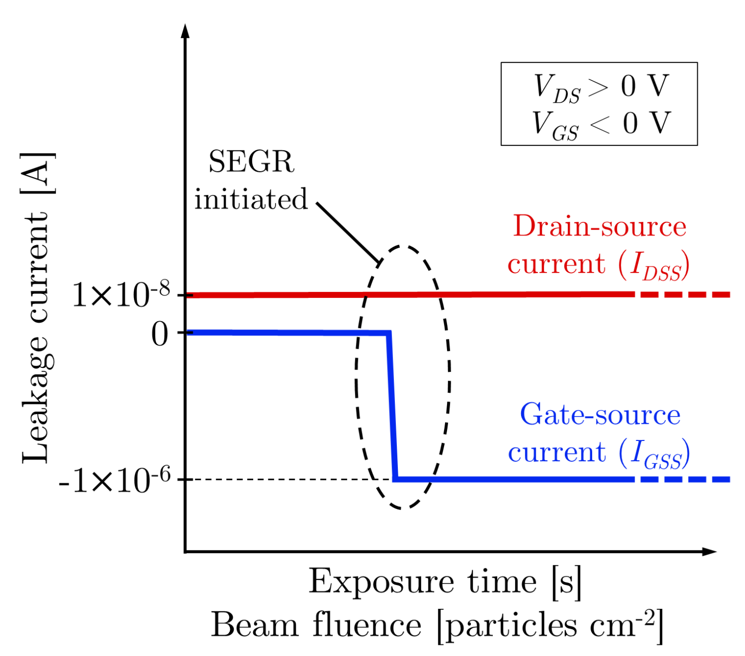
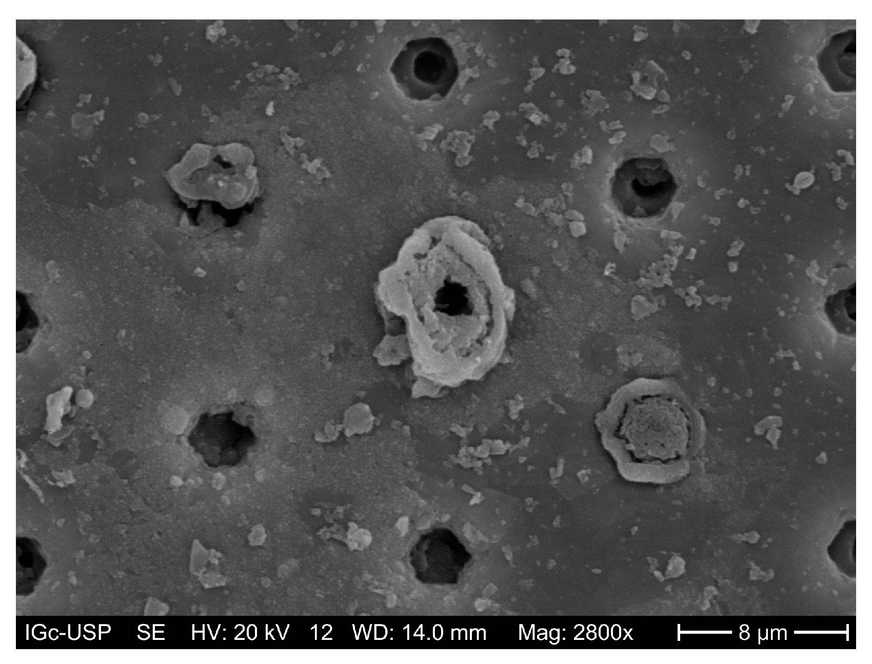
3.6. Destructive Effects: Single-Event Gate Rupture and Single-Event Burnout
3.6.1. Single-Event Gate Rupture (SEGR)
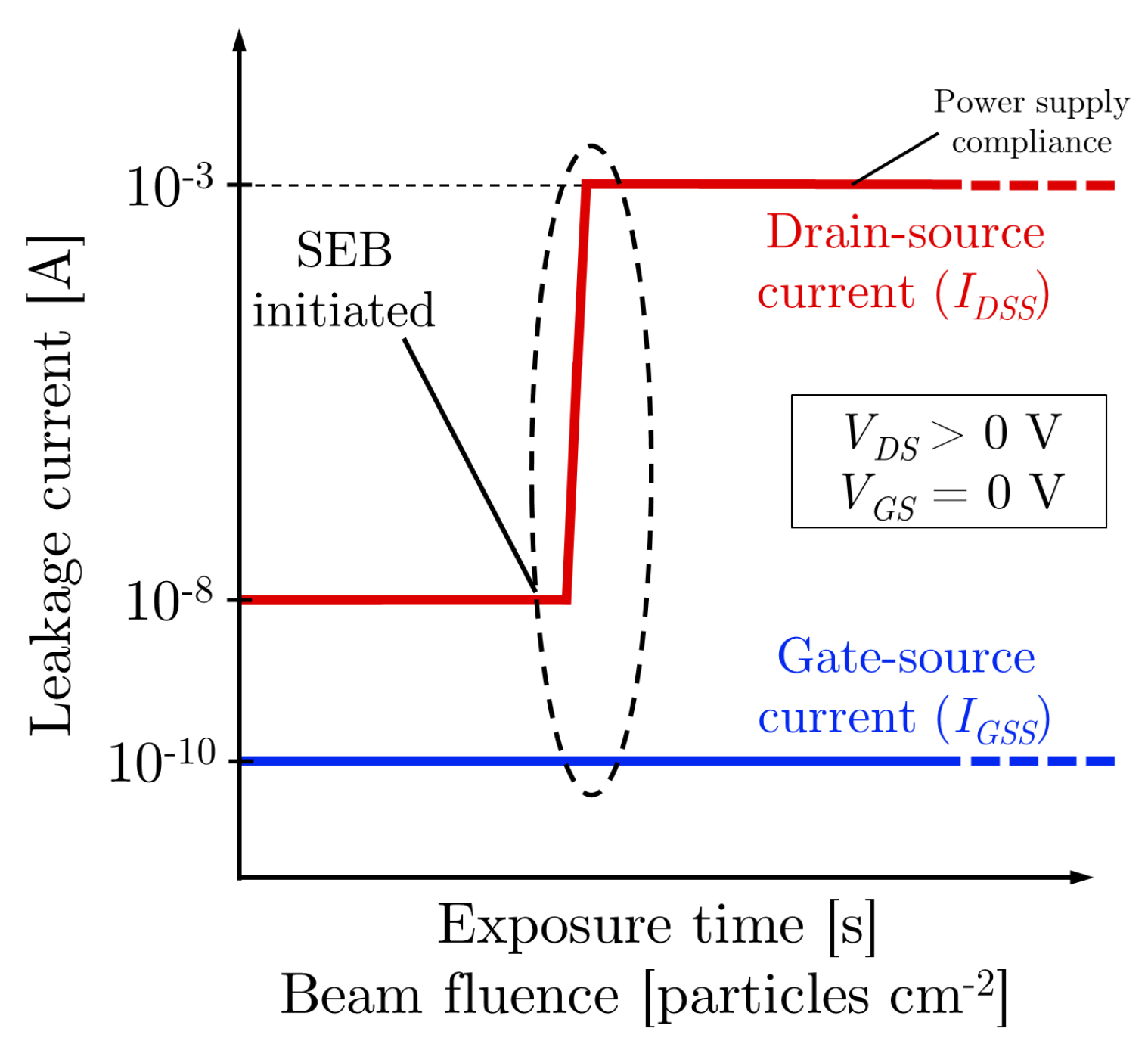
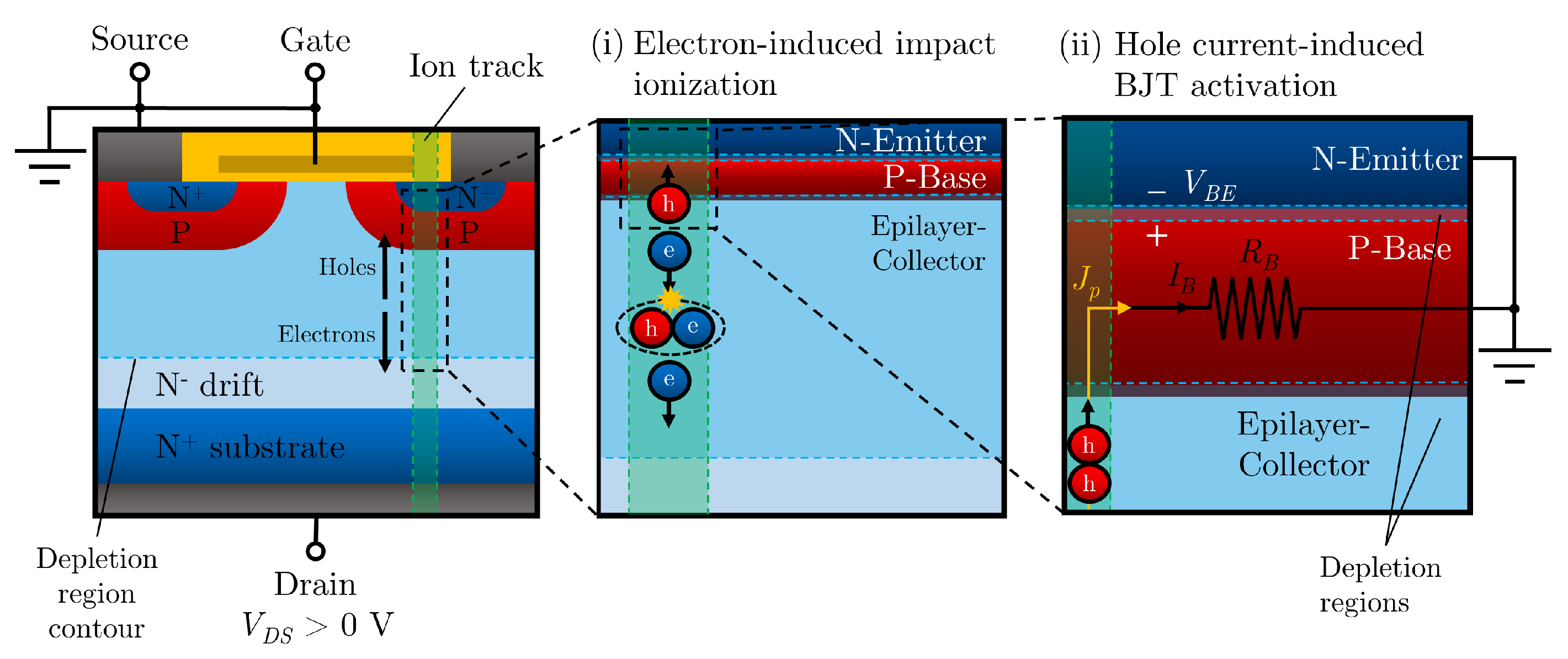
3.6.2. Single-Event Burnout
3.7. Neutron Secondary Effects
4. Impacts on Reliability in Harsh Environments
4.1. Power Systems
- De-rating: Typically consists in reducing the operating bias by 25% from the destructive SEE onset, preventing or eliminating the occurrence of destructive SEEs.
- Hardening by design: Structural and process modifications can improve radiation hardness, often at the cost of electrical performance [123]. For instance, SEB robustness in BJTs and MOSFETs can be improved by reducing the parasitic base–emitter resistance and lowering emitter current injection efficiency [158], as well as incorporating optimized buffer layers [159]. SEGR robustness can be improved by reducing neck width and implementing alternative stripe geometries [160].
4.2. Digital Circuits
- Layout- and electrical-level techniques:
- –
- Built-in current sensors (BICSs) are used to detect soft errors by monitoring currents in the bulk region of transistors. These sensors can differentiate ionization events, which cause sharp current spikes, from regular circuit activity. Bulk-BICSs detect SETs with a slight delay, which depends on the number of transistors connected, the intensity of the SET, and the calibration for SET signals. Once an SET is detected, the control logic can perform a fault-tolerant technique. The detection of SETs can be performed even with the use of neural networks [166].
- –
- Transistor resizing is used to increase the capacitance at sensitive nodes, thereby raising the critical charge level required to cause an SET. By increasing the capacitance at these nodes, the circuit becomes less susceptible to radiation-induced errors. However, resizing must be performed carefully to avoid performance and power drawbacks.
- Logic-level techniques:
- –
- Hardware redundancy, such as duplication with comparison (DWC), where a module is duplicated and the outputs are compared. However, DWC can only indicate that an error has occurred, not which specific part of the logic failed. Parity checking can be used for improved robustness. A more advanced approach is N-modular redundancy (N-MR), where multiple modules (usually three in the case of Triple Modular Redundancy, TMR) are used and a majority voter selects the correct output [167,168,169].
- –
- Time redundancy techniques, such as using two flip-flops with delayed clock signals to capture the output at two distinct times, enabling SET detection. A more advanced approach, full-time redundancy, uses three clocked latches with a majority voter to select the correct output based on multiple observations over time. However, in nanometer technologies, this technique faces challenges when SET pulses last longer than the clock cycle, limiting its effectiveness. The time delay between clocks must be sufficient to capture SETs, but the method becomes impractical when SET durations are comparable to the clock period [170].
- –
- Memory cells can be hardened against SEUs with additional transistors or resistors that allow for the recovery of the stored value when an upset occurs. These techniques typically involve slowing the regenerative feedback of a memory cell or adding feedback mechanisms to restore corrupted data [171]. New materials and technologies for memories also represent a possibility for increasing reliability in harsh environments [172,173]
- –
- Error-correcting codes (ECCs) use information redundancy to mitigate soft errors (SEUs) in integrated circuits. They are primarily used in memory arrays but can also be applied to microprocessor registers and other small memory structures. ECCs can be implemented on hardware or software. Simple ECC methods, like Hamming code, can detect double-bit errors and correct single-bit errors at the cost of including extra check bits, while more complex codes can address multi-bit errors, implemented at hardware and software levels.
5. Concluding Remarks
Author Contributions
Funding
Conflicts of Interest
References
- Ziegler, J.F.; Curtis, H.W.; Muhlfeld, H.P.; Montrose, C.J.; Chin, B.; Nicewicz, M.; Russell, C.A.; Wang, W.Y.; Freeman, L.B.; Hosier, P.; et al. IBM experiments in soft fails in computer electronics (1978–1994). IBM J. Res. Dev. 1996, 40, 3–18. [Google Scholar] [CrossRef]
- Heidel, D.; Rodbell, K.; Cannon, E.; Cabral, J.C.; Gordon, M.; Oldiges, P.; Tang, H.H.K. Alpha-particle-induced upsets in advanced CMOS circuits and technology. IBM J. Res. Dev. 2008, 52, 225–232. [Google Scholar] [CrossRef]
- Baumann, R.C. Soft Errors in Advanced Semiconductor Devices—Part I: The Three Radiation Sources. IEEE Trans. Device Mater. Reliab. 2001, 1, 17–22. [Google Scholar] [CrossRef]
- Schwank, J.R.; Shaneyfelt, M.R.; Dodd, P.E. Radiation Hardness Assurance Testing of Microelectronic Devices and Integrated Circuits: Radiaiton Environments, Physical Mechanisms and Foundations for Hardness Assurance; Document 2008-6851P; Sandia National Laboratories: Albuquerque, NM, USA, 2008. [Google Scholar]
- Leroy, C.; Rancoita, P.G. Principles of Radiation Interaction in Matter and Detection, 2nd ed.; World Scientific: Hackensack, NJ, USA, 2009. [Google Scholar]
- Ziegler, J.F. Terrestrial cosmic rays. IBM J. Res. Dev. 1996, 40, 19–39. [Google Scholar] [CrossRef]
- Di Giovanni, F. Silicon Carbide: Physics, Manufacturing, and Its Role in Large-Scale Vehicle Electrification. Chips 2023, 2, 209–222. [Google Scholar] [CrossRef]
- Tian, W.; Ma, T.; Liu, X. TSV Technology and High-Energy Heavy Ions Radiation Impact Review. Electronics 2018, 7, 112. [Google Scholar] [CrossRef]
- Gordon, M.; Rodbell, K.; Heidel, D.; Cabral, J.C.; Cannon, E.; Reinhardt, D. Single-Event-Upset and alpha-particle emission rate measurement techniques. IBM J. Res. Dev. 2008, 52, 225–232. [Google Scholar] [CrossRef]
- Fleetwood, D.M. Radiation Effects in a Post-Moore World. IEEE Trans. Nucl. Sci. 2021, 68, 509–545. [Google Scholar] [CrossRef]
- Benfica, J.; Green, B.; Porcher, B.C.; Poehls, L.B.; Vargas, F.; Medina, N.H.; Added, N.; De Aguiar, V.A.P.; Macchione, E.L.A.; Aguirre, F.; et al. Analysis of SRAM-Based FPGA SEU Sensitivity to Combined EMI and TID-Imprinted Effects. IEEE Trans. Nucl. Sci. 2016, 63, 1294–1300. [Google Scholar] [CrossRef]
- Zinkle, S.; Snead, L. Opportunities and limitations for ion beams in radiation effects studies: Bridging critical gaps between charged particle and neutron irradiations. Scr. Mater. 2018, 143, 154–160. [Google Scholar] [CrossRef]
- Zhang, Y.; Xue, H.; Zarkadoula, E.; Sachan, R.; Ostrouchov, C.; Liu, P.; Wang, X.l.; Zhang, S.; Wang, T.S.; Weber, W.J. Coupled electronic and atomic effects on defect evolution in silicon carbide under ion irradiation. Curr. Opin. Solid State Mater. Sci. 2017, 21, 285–298. [Google Scholar] [CrossRef]
- Zeng, Q.; Yang, Z.; Wang, X.; Li, S.; Gao, F. Research Progress on Radiation Damage Mechanism of SiC MOSFETs Under Various Irradiation Conditions. IEEE Trans. Electron Devices 2024, 71, 1718–1727. [Google Scholar] [CrossRef]
- Vogl, T.; Sripathy, K.; Sharma, A.; Reddy, P.; Sullivan, J.; Machacek, J.R.; Zhang, L.; Karouta, F.; Buchler, B.C.; Doherty, M.W.; et al. Radiation tolerance of two-dimensional material-based devices for space applications. Nat. Commun. 2019, 10, 1202. [Google Scholar] [CrossRef]
- Lutz, G. Semiconductor Radiation Detectors; Springer: Berlin/Heidelberg, Germany, 1999. [Google Scholar]
- Silveira, M.A.G.; Melo, M.A.A.; Aguiar, V.A.P.; Rallo, A.; Santos, R.B.B.; Medina, N.H.; Added, N.; Seixas, L.E.; Leite, F.G.; Cunha, F.G.; et al. A Commercial off-the-shelf pMOS Transistor as X-ray and Heavy Ion Detector. J. Phys. Conf. Ser. 2015, 630, 012012. [Google Scholar] [CrossRef]
- Vilas Boas, A.C.; Gabriel Alberton, S.; Medina, N.; Angelo Paulino, V.; Assis Melo, M.A.; Baginski Santos, R.; Giacomini, R.; Cavalcante, T.; Galhardo Vaz, R.; Junior, E.; et al. Reliability analysis of gamma- and X-ray TID effects, on a commercial AlGaN/GaN based FET. JICS 2021, 16, 1–7. [Google Scholar] [CrossRef]
- Fleetwood, D.M. Total-Ionizing-Dose Effects, Border Traps, and 1/F Noise Emerging MOS Technologies. IEEE Trans. Nucl. Sci. 2020, 67, 1216–1240. [Google Scholar] [CrossRef]
- Stoller, R.; Toloczko, M.; Was, G.; Certain, A.; Dwaraknath, S.; Garner, F. On the use of SRIM for computing radiation damage exposure. Nucl. Instrum. Methods Phys. Res. Sect. B Beam Interact. Mater. Atoms 2013, 310, 75–80. [Google Scholar] [CrossRef]
- Duzellier, S. Radiation effects on electronic devices in space. Aerosp. Sci. Technol. 2005, 9, 93–99. [Google Scholar] [CrossRef]
- Pan, S.; Feng, S.; Li, X.; Zheng, X.; Lu, X.; Hu, C.; Shao, G.; Lin, G. Analysis of the Effects of High-Energy Electron Irradiation of GaN High-Electron-Mobility Transistors Using the Voltage-Transient Method. IEEE Trans. Electron Devices 2021, 68, 3968–3973. [Google Scholar] [CrossRef]
- Soibel, A.; Rafol, S.B.; Khoshakhlagh, A.; Nguyen, J.; Hoglund, L.; Fisher, A.M.; Keo, S.A.; Ting, D.Z.Y.; Gunapala, S.D. Proton radiation effect on performance of InAs/GaSb complementary barrier infrared detector. Appl. Phys. Lett. 2015, 107, 261102. [Google Scholar] [CrossRef]
- Yuan, Y.; Zhou, S.; Wang, X. Modulating properties by light ion irradiation: From novel functional materials to semiconductor power devices. J. Semicond. 2022, 43, 063101. [Google Scholar] [CrossRef]
- Arnold, K.P.; Musibau, S.; Dattilo, H.M.; Sutton, H.J.; Frankowski, S.L.; Berciano, M.; Zhang, E.X.; McCurdy, M.W.; Crespillo, M.L.; Hattar, K.; et al. Displacement Damage and Ionization Effects on Waveguide-Integrated Germanium-Silicon PIN Photodiodes. IEEE Trans. Nucl. Sci. 2025, 1. [Google Scholar] [CrossRef]
- Xi, J.; Zhang, H.; Su, R.; Wei, S.; Hu, X.; Queylat, B.; Kim, T.; Couet, A.; Szlufarska, I. Coupling of radiation and grain boundary corrosion in SiC. NPJ Mater. Degrad. 2024, 8, 16. [Google Scholar] [CrossRef]
- Guazzelli, M.; Avanzi, L.; Aguiar, V.; Vilas-Boas, A.; Alberton, S.; Masunaga, S.; Chinaglia, E.; Araki, K.; Nakamura, M.; Toyama, M.; et al. Effects of neutron radiation on the thermal conductivity of highly oriented pyrolytic graphite. Diam. Relat. Mater. 2025, 151, 111803. [Google Scholar] [CrossRef]
- Ullah, M.W.; Zhang, Y.; Sellami, N.; Debelle, A.; Bei, H.; Weber, W.J. Evolution of irradiation-induced strain in an equiatomic NiFe alloy. Scr. Mater. 2017, 140, 35–39. [Google Scholar] [CrossRef]
- Baubekova, G.; Akilbekov, A.; Feldbach, E.; Grants, R.; Manika, I.; Popov, A.; Schwartz, K.; Vasil’chenko, E.; Zdorovets, M.; Lushchik, A. Accumulation of radiation defects and modification of micromechanical properties under MgO crystal irradiation with swift 132Xe ions. Nucl. Instrum. Methods Phys. Res. Sect. B Beam Interact. Mater. Atoms 2020, 463, 50–54. [Google Scholar] [CrossRef]
- Tang, H.H.K. Nuclear physics of cosmic ray interaction with semiconductor materials: Particle-induced soft errors from a physicist’s perspective. IBM J. Res. Dev. 1996, 40, 91–108. [Google Scholar] [CrossRef]
- Sierawski, B.D.; Warren, K.M.; Reed, R.A.; Weller, R.A.; Mendenhall, M.M.; Schrimpf, R.D.; Baumann, R.C.; Zhu, V. Contribution of Low Energy (<10 MeV) Neutrons to Upset Rate in a 65 nm SRAM. In Proceedings of the 2010 IEEE International Reliability Physics Symposium, Anaheim, CA, USA, 2–6 May 2010; pp. 4B.2.1–4B.2.5. [Google Scholar]
- Rodbell, K.; Heidel, D.; Tang, H.; Gordon, M.; Oldiges, P.; Murray, C. Low-energy proton-induced single-event-upsets in 65 nm node, silicon-on-insulator, latches and memory cells. IEEE Trans. Nucl. Sci. 2007, 54, 2474–2479. [Google Scholar] [CrossRef]
- Barak, J.; Murat, M.; Akkerman, A. SEU due to electrons in silicon devices with nanometric sensitive volumes and small critical charge. Nucl. Instrum. Methods Phys. Res. 2012, 287, 113–119. [Google Scholar] [CrossRef]
- Velazco, R.; Fouillat, P.; Reis, R.A.d.L. Radiation Effects on Embedded Systems; Springer: Dordrecht, The Netherlands, 2007. [Google Scholar]
- Petersen, E.L. Dosimetry Comparisons Between Various Single Event Test Facilities. IEEE Trans. Nucl. Sci. 2010, 57, 3477–3482. [Google Scholar] [CrossRef]
- Medina, N.H.; de Aguiar, V.Â.; Added, N.; Aguirre, F.; Macchione, E.L.; Alberton, S.G.; da Silva, M.A.; Benfica, J.; Vargas, F.L.; Porcher, B. Experimental Setups for Single Event Effect Studies. JNP 2016, 4, 13–23. [Google Scholar] [CrossRef]
- Aguiar, V.; Added, N.; Medina, N.; Macchione, E.; Tabacniks, M.; Aguirre, F.; Silveira, M.; Santos, R.; Seixas, L. Experimental setup for Single Event Effects at the São Paulo 8UD Pelletron Accelerator. Nucl. Instrum. Methods Phys. Res. Sect. B Beam Interact. Mater. Atoms 2014, 332, 397–400. [Google Scholar] [CrossRef]
- F1192-00; Standard Guide for the Measurement of Single Event Phenomena (SEP) Induced by Heavy Ion Irradiation of Semiconductor Devices. ASTM Standard. American Society for Testing and Materials: West Conshohocken, PA, USA, 2006.
- European Space Agency. Single Event Effects Test Method and Guidelines, ESCC Basic Specification No. 25100; Technical Report; European Space Agency: Paris, France, 2014. [Google Scholar]
- ESA/SCC Basic Specification 22900; Total Dose Steady-State Irradiation Test Method. ESA/SCC Basic Specification 1. European Space Agency: Paris, France, 1995.
- JEDEC-JESD57A; Test Procedures for the Measurement of Single-Event Effects in Semiconductor Devices from Heavy-Ion Irradiation. Technical Report. JEDEC Solid State Technology Association: Arlington County, VA, USA, 2017.
- Ziegler, J.F.; Biersack, J.; Ziegler, M. SRIM: The Stopping and Range of Ions in Matter; SRIM Co.: Hyderabad, India, 2008. [Google Scholar]
- Wyss, J.; Bisello, D.; Pantano, D. SIRAD: An irradiation facility at the LNL Tandem accelerator for radiation damage studies on semiconductor detectors and electronic devices and systems. Nucl. Instrum. Methods Phys. Res. A 2001, 462, 426–434. [Google Scholar] [CrossRef]
- Mattiazzo, S.; Bisello, D.; Giubilato, P.; Kaminsky, A.; Pantano, D.; Silvestrin, L.; Tessaro, M.; Wyss, J. First results in micromapping the sensivity to SEE of an electronic device in a SOI technology at the LNL IEEM. Nucl. Instrum. Methods Phys. Res. A 2011, 658, 125–128. [Google Scholar] [CrossRef]
- Silvestrin, L.; Bisello, D.; Busatto, G.; Giubilato, P.; Iannuzzo, F.; Mattiazzo, S.; Pantano, D.; Sanseverino, A.; Tessaro, M.; Velardi, F.; et al. A time-resolved IBICC experiment using the IEEMof the SIRAD facility. Nucl. Instrum. Methods Phys. Res. B 2012, 273, 234–236. [Google Scholar] [CrossRef]
- Palomo, F.R.; Morilla, Y.; Mogollón, J.M.; García-López, J.; Labrador, J.A.; Aguirre, M.A. Early works on the nuclear microprobe for microelectronics irradiation tests at the CEICI (Sevilla, Spain). Nucl. Instrum. Methods Phys. Res. B 2011, 269, 2210–2216. [Google Scholar] [CrossRef]
- Aguiar, V.A.P.; Medina, N.H.; Added, N.; Macchione, E.L.A.; Alberton, S.G.; Leite, A.R.; Aguirre, F.R.; Ribas, R.V.; Perego, C.C.; Fagundes, L.M.; et al. SAFIIRA: A heavy-ion multi-purpose irradiation facility in Brazil. Rev. Sci. Instrum. 2020, 91, 053301. [Google Scholar] [CrossRef]
- Tonfat, J.; Lima Kastensmidt, F.; Artola, L.; Hubert, G.; Medina, N.H.; Added, N.; Aguiar, V.A.P.; Aguirre, F.; Macchione, E.L.A.; Silveira, M.A.G. Analyzing the Influence of the Angles of Incidence and Rotation on MBU Events Induced by Low LET Heavy Ions in a 28-nm SRAM-Based FPGA. IEEE Trans. Nucl. Sci. 2017, 64, 2161–2168. [Google Scholar] [CrossRef]
- Petersen, E. Single Event Effects in Aerospace; John Wiley & Sons: Hoboken, NJ, USA, 2011. [Google Scholar]
- Gu, S.; Liu, J.; Bi, J.; Zhao, F.; Zhang, Z.; Xi, K.; Peng, K.; Zhang, Y. The Impacts of Heavy Ion Energy on Single Event Upsets in SOI SRAMs. IEEE Trans. Nucl. Sci. 2018, 65, 1091–1100. [Google Scholar] [CrossRef]
- Alia, R.G.; Bahamonde, C.; Brandenburg, S.; Brugger, M.; Daly, E.; Ferlet-Cavrois, V.; Gaillard, R.; Hoeffgen, S.; Menicucci, A.; Metzger, S.; et al. Sub-LET Threshold SEE Cross Section Dependency with Ion Energy. IEEE Trans. Nucl. Sci. 2015, 62, 2797–2806. [Google Scholar] [CrossRef]
- Petersen, E.L. Single-Event Data Analysis. IEEE Trans. Nucl. Sci. 2008, 55, 2819–2841. [Google Scholar] [CrossRef]
- Inguimbert, C.; Duzellier, S.; Nuns, T.; Bezerra, F. Using Subthreshold Heavy Ion Upset Cross Section to Calculate Proton Sensitivity. IEEE Trans. Nucl. Sci. 2007, 54, 2394–2399. [Google Scholar] [CrossRef]
- Connell, L.; McDaniel, P.; Prinja, A.; Sexton, F. Modeling the Heavy Ion Upset Cross Section. IEEE Trans. Nucl. Sci. 1995, 42. [Google Scholar] [CrossRef]
- Dodd, P.E. Physics-based simulation of single-event effects. IEEE Trans. Device Mater. Reliab. 2005, 5, 343–357. [Google Scholar] [CrossRef]
- Srinivasan, G.; Tang, H.; Murley, P. Parameter-free, predictive modeling of single event upsets due to protons, neutrons and pions in terrestrial cosmic rays. IEEE Trans. Nucl. Sci. 1994, 41, 2063–2070. [Google Scholar] [CrossRef]
- Tang, H.; Cannon, E.H. SEMM-2: A Modeling System for Single Event Upset Analysis. IEEE Trans. Nucl. Sci. 2004, 51, 3342–3348. [Google Scholar] [CrossRef]
- Li, Y.; Yu, D.; Zhang, Q.; Cai, Z.; Jia, X.; Wang, Y. Qcrit-independent model method for proton SEU analysis. Microelectron. Reliab. 2019, 93, 72–80. [Google Scholar] [CrossRef]
- Murat, M.; Akkerman, A.; Barak, J. Electron and ion tracks in silicon: Spatial and temporal evolution. IEEE Trans. Nucl. Sci. 2008, 55, 3046–3054. [Google Scholar] [CrossRef]
- Wrobel, F.; Hubert, G.; Iacconi, P. A semi-empirical approach for heavy ion SEU cross section calculations. IEEE Trans. Nucl. Sci. 2006, 53, 3271–3276. [Google Scholar] [CrossRef]
- Sogoyan, A.; Chumakov, A.; Smolin, A.; Ulanova, A.; Boruzdina, A. A simple analytical model of single-event upsets in bulk CMOS. Nucl. Instrum. Methods Phys. Res. B 2017, 400, 31–36. [Google Scholar] [CrossRef]
- Normand, E. Single-event effects in avionics. IEEE Trans. Nucl. Sci. 1996, 43, 461–474. [Google Scholar] [CrossRef]
- Normand, E. Single event upset at ground level. IEEE Trans. Nucl. Sci. 1996, 43, 2742–2750. [Google Scholar] [CrossRef]
- JESD89-3B; Test Method For Beam Accelerated Soft Error Rate. EIA/JEDEC Standard. Electronic Industries Association: Arlington County, VA, USA, 2021.
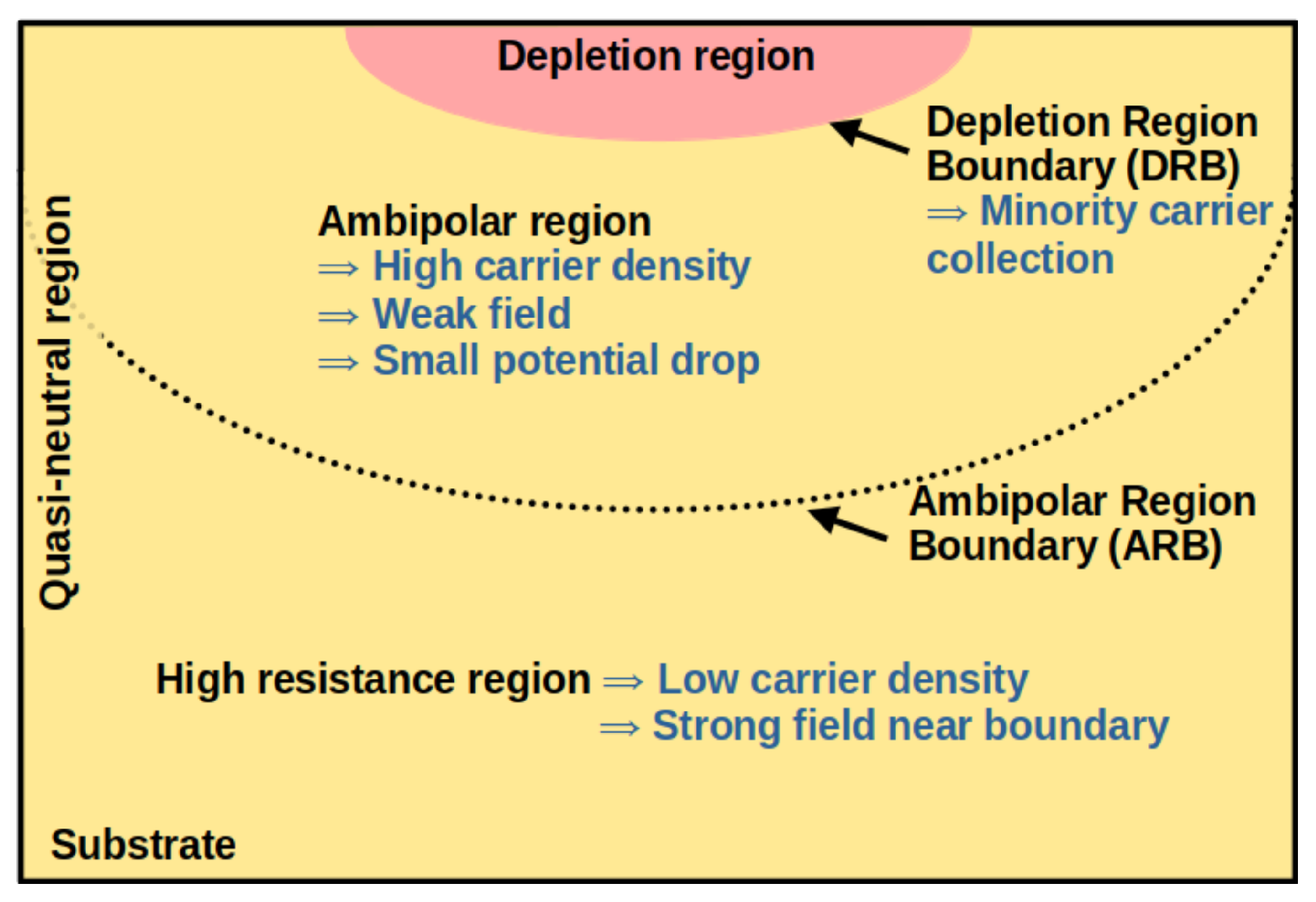
- McLean, F.; Oldham, T. Charge funneling in n- and p-type Si substrates. IEEE Trans. Nucl. Sci. 1982, 29, 2017–2023. [Google Scholar] [CrossRef]
- Oldham, T.R.; McLean, F.B.; Hartman, J.M. Revised funnel calculations for heavy particles with high dE/dx. IEEE Trans. Nucl. Sci. 1986, 33, 1646–1650. [Google Scholar] [CrossRef]
- Liu, J.; Yan, S.; Xue, J.; Wang, Y. Comparison of ionization track structure models for electronic devices of different sizes. Nucl. Instrum. Methods Phys. Res. B 2019, 444, 43–49. [Google Scholar] [CrossRef]
- Edmonds, L. Electric currents through ion tracks in silicon devices. IEEE Trans. Nucl. Sci. 1998, 45, 3153–3164. [Google Scholar] [CrossRef]
- Ahlbin, J.; Gadlage, M.; Atkinson, N.; Narasimham, B.; Bhuva, B.; Witulski, A.; Holman, W.; Eaton, P.; Massengill, L. Effect of Multiple-Transistor Charge Collection on Single-Event Transient Pulse Widths. IEEE Trans. Device Mater. Reliab. 2011, 11, 401–406. [Google Scholar] [CrossRef]
- Musseau, O. Charge collection and SEU mechanisms. Radiat. Phys. Chem. 1994, 43, 151–163. [Google Scholar] [CrossRef]
- Hu, C. Alpha-particle-induced field and enhanced collection of carriers. IEEE Electron Device Lett. 1982, 3, 31–34. [Google Scholar] [CrossRef]
- Takada, M.; Nunomiya, T.; Ishikura, T.; Nakamura, T. Charge-Collection Length Induced by Proton and Alpha Particle Injected Into Silicon Detectors Due to Funneling Effect. IEEE Trans. Nucl. Sci. 2009, 56, 337–345. [Google Scholar] [CrossRef]
- Aguiar, V.A.P.; Medina, N.H.; Added, N.; Alberton, S.G.; Macchione, E.L.A.; Guazzelli, M.A.; Melo, M.A.A.; Oliveira, J.A.; Giacomini, R.C.; Aguirre, F.R.; et al. Evaluation of Funnel Models on Calculation of Ion-Induced Collected Charge. IEEE Trans. Electron Devices 2025, 72, 31–36. [Google Scholar] [CrossRef]
- Edmonds, L.D. A theoretical analysis of steady-state charge collection in simple diodes under high-injection conditions. IEEE Trans. Nucl. Sci. 2010, 57, 818–830. [Google Scholar] [CrossRef]
- Edmonds, L.D. A theoretical analysis of the role of ambipolar diffusion in charge-carrier transport in a quasi-neutral region under high injection. IEEE Trans. Nucl. Sci. 2011, 58, 2459–2469. [Google Scholar] [CrossRef]
- Edmonds, L.D. A proposed transient version of the ADC charge-collection model tested against TCAD. IEEE Trans. Nucl. Sci. 2011, 58, 296–304. [Google Scholar] [CrossRef]
- Hooten, N.; Edmonds, L.; Bennett, W.; Ahlbin, J.; Dodds, N.; Reed, R.; Schrimpf, R.; Weller, R. The significance of high-level carrier generation conditions for charge collection in irradiated devices. IEEE Trans. Nucl. Sci. 2012, 59, 2710–2721. [Google Scholar] [CrossRef]
- Assis, T.; Ni, K.; Kauppila, J.; Bhuva, B.; Schrimpf, R.; Massengill, L.; Wen, S.; Wong, R.; Slayman, C. Estimation of single-event-induced collected charge for multiple transistors using analytical expressions. IEEE Trans. Nucl. Sci. 2015, 62, 2853–2859. [Google Scholar] [CrossRef]
- Choo, K.; Muniandy, S.; Woon, K.; Gan, M.; Ong, D. Modeling anomalous charge carrier transport in disordered organic semiconductors using the fractional drift-diffusion equation. Org. Electron. 2017, 41, 157–165. [Google Scholar] [CrossRef]
- Ma, H.; Wang, W.; Cai, Y.; Wang, Z.; Zhang, T.; Feng, Q.; Chen, Y.; Zhang, C.; Zhang, J.; Hao, Y. Analysis of single event effects by heavy ion irradiation of Ga2O3 metal–oxide–semiconductor field-effect transistors. J. Appl. Phys. 2023, 133, 085701. [Google Scholar] [CrossRef]
- Ni, K.; Zhang, E.X.; Samsel, I.K.; Schrimpf, R.D.; Reed, R.A.; Fleetwood, D.M.; Sternberg, A.L.; McCurdy, M.W.; Ren, S.; Ma, T.P.; et al. Charge Collection Mechanisms in GaAs MOSFETs. IEEE Trans. Nucl. Sci. 2015, 62, 2752–2759. [Google Scholar] [CrossRef]
- Boorboor, S.; Feghhi, S.; Jafari, H. Funneling effect of alpha particles on the charge collection efficiency in N type silicon surface barrier detector. Nucl. Instrum. Methods Phys. Res. B 2014, 325, 1–4. [Google Scholar] [CrossRef]
- Lopez, J.G.; Jimenez-Ramos, M.; Rodrigues-Ramos, M.; Forneris, J.; Ceballos, J. An upgraded drift-diffusion model for evaluating the carrier lifetimes in radiation-damaged semiconductor detectors. Nucl. Instrum. Methods Phys. Res. B 2016, 371, 294–297. [Google Scholar] [CrossRef]
- Kunc, J.; Praus, P.; Belas, E.; Dědič, V.; Pekárek, J.; Grill, R. Efficient Charge Collection in Coplanar-Grid Radiation Detectors. Phys. Rev. Appl. 2018, 9, 054020. [Google Scholar] [CrossRef]
- Ziegler, J.F.; Ziegler, M.D.; Biersack, J.P. SRIM—The Stopping and Range of Ions in Matter (2010). Nucl. Instrum. Methods Phys. Res. Sect. B Beam Interact. Mater. Atoms 2010, 268, 1818–1823. [Google Scholar] [CrossRef]
- Agostinelli, S.; Allison, J.; Amako, K.; Apostolakis, J.; Araujo, H.; Arce, P.; Asai, M.; Axen, D.; Banerjee, S.; Barrand, G.; et al. Geant4—A simulation toolkit. Nucl. Instrum. Methods Phys. Res. Sect. A Accel. Spectrometers Detect. Assoc. Equip. 2003, 506, 250–303. [Google Scholar] [CrossRef]
- Lucsányi, D.; Alía, R.G.; Biłko, K.; Cecchetto, M.; Fiore, S.; Pirovano, E. G4SEE: A Geant4-based Single Event Effect Simulation Toolkit and its Validation Through Monoenergetic Neutron Measurements. IEEE Trans. Nucl. Sci. 2022, 69, 273–281. [Google Scholar] [CrossRef]
- Wu, Y.C.; Jhan, Y.R. Introduction of Synopsys Sentaurus TCAD Simulation. In 3D TCAD Simulation for CMOS Nanoeletronic Devices; Springer: Singapore, 2018; pp. 1–17. [Google Scholar] [CrossRef]
- ATLAS User’s Manual. Available online: https://www.eng.buffalo.edu/~wie/silvaco/atlas_user_manual.pdf (accessed on 3 March 2025).
- Michez, A.; Dhombres, S.; Boch, J. ECORCE: A TCAD Tool for Total Ionizing Dose and Single Event Effect Modeling. IEEE Trans. Nucl. Sci. 2015, 62, 1516–1527. [Google Scholar] [CrossRef]
- Rossi, C.; Chatel, A.; Sallese, J. Modeling Funneling Effect with Generalized Devices for SPICE Simulation of Soft Errors. IEEE Trans. Electron Devices 2021, 68, 2633–2640. [Google Scholar] [CrossRef]
- Aneesh, Y.M.; Sriram, S.R.; Pasupathy, K.R.; Bindu, B. An Analytical Model of Single-Event Transients in Double-Gate MOSFET for Circuit Simulation. IEEE Trans. Electron Devices 2019, 66, 3710–3717. [Google Scholar] [CrossRef]
- TCAD Central. Available online: https://tcadcentral.com/index.html (accessed on 3 March 2025).
- King, M.P.; Reed, R.A.; Weller, R.A.; Mendenhall, M.H.; Schrimpf, R.D.; Sierawski, B.D.; Sternberg, A.L.; Narasimham, B.; Wang, J.K.; Pitta, E.; et al. Electron-Induced Single-Event Upsets in Static Random Access Memory. IEEE Trans. Nucl. Sci. 2013, 60, 4122–4129. [Google Scholar] [CrossRef]
- Spieler, H. Semiconductor Detector Systems; Series on semiconductor science and technology; Oxford University Press: Oxford, UK, 2005. [Google Scholar] [CrossRef]
- Knoll, G.F. Radiation Detection and Measurement; Wiley: New York, NY, USA, 2000. [Google Scholar]
- Sze, S.M. Physics of Semiconductor Devices, 2nd ed.; John Wiley & Sons: Hoboken, NJ, USA, 1981. [Google Scholar]
- Deen, M.J.; Pascal, F. Electrical Characterization of Semiconductor Materials and Devices. In Springer Handbook of Electronic and Photonic Materials; Kasap, S., Capper, P., Eds.; Springer International Publishing: Cham, Switzerland, 2017; p. 1. [Google Scholar] [CrossRef]
- Dalla Betta, G.F.; Ye, J. Silicon Radiation Detector Technologies: From Planar to 3D. Chips 2023, 2, 83–101. [Google Scholar] [CrossRef]
- Turchetta, R.; Fant, A.; Gasiorek, P.; Esbrand, C.; Griffiths, J.; Metaxas, M.; Royle, G.; Speller, R.; Venanzi, C.; van der Stelt, P.; et al. CMOS Monolithic Active Pixel Sensors (MAPS): Developments and future outlook. Nucl. Instrum. Methods Phys. Res. Sect. A Accel. Spectrometers Detect. Assoc. Equip. 2007, 582, 866–870. [Google Scholar] [CrossRef]
- Korol, I. Beam test characterization of CMS silicon pixel detectors for the phase-1 upgrade. Nucl. Instrum. Methods Phys. Res. Sect. A Accel. Spectrometers Detect. Assoc. Equip. 2015, 796, 64–67. [Google Scholar] [CrossRef]
- Zaťko, B.; Zápražný, Z.; Jakůbek, J.; Šagátová, A.; Boháček, P.; Sekáčová, M.; Korytár, D.; Nečas, V.; Žemlička, J.; Mora, Y.; et al. Imaging performance of a Timepix detector based on semi-insulating GaAs. J. Instrum. 2018, 13, C01034. [Google Scholar] [CrossRef]
- Amendolia, S.; Bertolucci, E.; Bisogni, M.; Bottigli, U.; Ciocci, M.; Conti, M.; Delogu, P.; Fantacci, M.; Maestro, P.; Marzulli, V.; et al. GaAs detector optimization for different medical imaging applications. Nucl. Instrum. Methods Phys. Res. Sect. A Accel. Spectrometers Detect. Assoc. Equip. 1999, 434, 14–17. [Google Scholar] [CrossRef]
- Šagátová, A.; Kubanda, D.; Zat’Ko, B.; Sedlačková, K.; Nečas, V.; Solar, M.; Granja, C. Semi-insulating GaAs based detector of fast neutrons produced by D-T nuclear reaction. J. Instrum. 2016, 11, C12002. [Google Scholar] [CrossRef]
- Wu, X.; Peltola, T.; Arsenovich, T.; Gädda, A.; Härkönen, J.; Junkes, A.; Karadzhinova, A.; Kostamo, P.; Lipsanen, H.; Luukka, P.; et al. Processing and characterization of epitaxial GaAs radiation detectors. Nucl. Instrum. Methods Phys. Res. Sect. A Accel. Spectrometers Detect. Assoc. Equip. 2015, 796, 51–55. [Google Scholar] [CrossRef]
- Chernykh, S.; Chernykh, A.; Didenko, S.; Baryshnikov, F.; Burtebayev, N.; Britvich, G.; Chubenko, A.; Guly, V.; Glybin, Y.; Zholdybayev, T.; et al. GaAs detectors with an ultra-thin Schottky contact for spectrometry of charged particles. Nucl. Instrum. Methods Phys. Res. Sect. A Accel. Spectrometers Detect. Assoc. Equip. 2017, 845, 52–55. [Google Scholar] [CrossRef]
- Pereira, M.S.; Aguiar, V.A.P.; Alberton, S.G.; Quivy, A.A. Response testing of Schottky-barrier GaAs detectors with alpha particles. J. Phys. Conf. Ser. 2022, 2340, 012050. [Google Scholar] [CrossRef]
- Tudisco, S.; Altana, C.; Boscardin, M.; Calcagno, L.; Ciampi, C.; Cirrone, G.A.; Fazzi, A.; Giove, D.; Gorini, G.; Labate, L.; et al. Silicon carbide for future intense luminosity nuclear physics investigations. Il Nuovo Cimento C 2019, 42, 1–4. [Google Scholar] [CrossRef]
- Puglisi, D.; Bertuccio, G. Silicon Carbide Microstrip Radiation Detectors. Micromachines 2019, 10, 835. [Google Scholar] [CrossRef]
- Lopez Paz, I.; Godignon, P.; Moffat, N.; Pellegrini, G.; Rafí, J.M.; Rius, G. Position-resolved charge collection of silicon carbide detectors with an epitaxially-grown graphene layer. Sci. Rep. 2024, 14, 10376. [Google Scholar] [CrossRef] [PubMed]
- Cappuzzello, F.; Agodi, C.; Calabretta, L.; Calvo, D.; Carbone, D.; Cavallaro, M.; Colonna, M.; Finocchiaro, P.; Iazzi, F.; Linares, R.; et al. The NUMEN Technical Design Report. Int. J. Mod. Phys. A 2021, 36, 2130018. [Google Scholar] [CrossRef]
- Azarov, A.; Fernandez, J.G.; Zhao, J.; Djurabekova, F.; He, H.; He, R.; Prytz, O.; Vines, L.; Bektas, U.; Chekhonin, P.; et al. Universal radiation tolerant semiconductor. Nat. Commun. 2023, 14, 4855. [Google Scholar] [CrossRef] [PubMed]
- Konovalov, V.; Roeder, B. Diamond ΔE-E telescope with an ultra-thin ΔE-diamond detector. Diam. Relat. Mater. 2024, 145, 111120. [Google Scholar] [CrossRef]
- He, Y.; Hadar, I.; Kanatzidis, M.G. Detecting ionizing radiation using halide perovskite semiconductors processed through solution and alternative methods. Nat. Photon. 2022, 16, 14–26. [Google Scholar] [CrossRef]
- Lang, F.; Jošt, M.; Frohna, K.; Köhnen, E.; Al-Ashouri, A.; Bowman, A.R.; Bertram, T.; Morales-Vilches, A.B.; Koushik, D.; Tennyson, E.M.; et al. Proton Radiation Hardness of Perovskite Tandem Photovoltaics. Joule 2020, 4, 1054–1069. [Google Scholar] [CrossRef]
- Tan, R.; Dryzhakov, B.; Charest, J.; Hu, B.; Ahmadi, M.; Lukosi, E. Improved Radiation Sensing with Methylammonium Lead Tribromide Perovskite Semiconductors. Nucl. Instrum. Methods Phys. Res. Sect. A Accel. Spectrometers Detect. Assoc. Equip. 2021, 986, 164710. [Google Scholar] [CrossRef]
- Pickel, J.C.; Blandford, J.T. Cosmic-ray-induced errors in MOS devices. IEEE Trans. Nucl. Sci. 1980, 27, 1006–1015. [Google Scholar] [CrossRef]
- Stephen, J.H.; Sanderson, T.K.; Mapper, D.; Farren, J.; Harboe-Sorensen, R.; Adams, L. Cosmic ray simulation experiments for the study of single event upsets and latch-up in CMOS memories. IEEE Trans. Nucl. Sci. 1983, 30, 4464–4469. [Google Scholar] [CrossRef]
- Waskiewicz, A.E.; Groninger, J.W.; Strahan, V.H.; Long, D.M. Burnout of power MOS transistors with heavy ions of Californium-252. IEEE Trans. Nucl. Sci. 1986, 33, 1710–1713. [Google Scholar] [CrossRef]
- Brucker, G.J.; Measel, P.; Oberg, D.; Wert, J.; Criswell, T. SEU sensitivity of power converters with MOSFETS in space. IEEE Trans. Nucl. Sci. 1987, 34, 1792–1795. [Google Scholar] [CrossRef]
- Pickel, J.C.; Blandford, J.T.; Waskiewicz, A.E.; Strahan, V.H. Heavy ion induced permanent damage in MNOS gate insulators. IEEE Trans. Nucl. Sci. 1985, 32, 4176–4179. [Google Scholar] [CrossRef]
- Ochoa, A.; Sexton, F.W.; Wrobel, T.F.; Hash, G.L.; Sokel, R.J. Snap-back: A stable regenerative breakdown mode of MOS devices. IEEE Trans. Nucl. Sci. 1983, 30, 4127–4130. [Google Scholar] [CrossRef]
- Sexton, F.W. Destructive single-event effects in semiconductor devices and ICs. IEEE Trans. Nucl. Sci. 2003, 50, 603–621. [Google Scholar] [CrossRef]
- Titus, J.L. An updated perspective of single event gate rupture and single event burnout in power MOSFETs. IEEE Trans. Nucl. Sci. 2013, 60, 1912–1928. [Google Scholar] [CrossRef]
- Wheatley, C.F.; Titus, J.L.; Burton, D.I. Single-event gate rupture in vertical power MOSFETs; an original empirical expression. IEEE Trans. Nucl. Sci. 1994, 41, 2152–2159. [Google Scholar] [CrossRef]
- Titus, J.; Wheatley, C.; Burton, D.; Mouret, I.; Allenspach, M.; Brews, J.; Schrimpf, R.; Galloway, K.; Pease, R. Impact of oxide thickness on SEGR failure in vertical power MOSFETs; development of a semi-empirical expression. IEEE Trans. Nucl. Sci. 1995, 42, 1928–1934. [Google Scholar] [CrossRef]
- Titus, J.L.; Wheatley, C.F. Experimental studies of single-event gate rupture and burnout in vertical power MOSFETs. IEEE Trans. Nucl. Sci. 1996, 43, 533–545. [Google Scholar] [CrossRef]
- Titus, J.; Wheatley, C.; Van Tyne, K.; Krieg, J.; Burton, D.; Campbell, A. Effect of ion energy upon dielectric breakdown of the capacitor response in vertical power MOSFETs. IEEE Trans. Nucl. Sci. 1998, 45, 2492–2499. [Google Scholar] [CrossRef]
- Titus, J.L.; Wheatley, C.F. SEE characterization of vertical DMOSFETs: An updated test protocol. IEEE Trans. Nucl. Sci. 2003, 50, 2341–2351. [Google Scholar] [CrossRef]
- Kuboyama, S.; Matsuda, S.; Kanno, T.; Ishii, T. Mechanism for single-event burnout of power MOSFETs and its characterization technique. IEEE Trans. Nucl. Sci. 1992, 39, 1698–1703. [Google Scholar] [CrossRef]
- Johnson, G.; Palau, J.; Dachs, C.; Galloway, K.; Schrimpf, R. A review of the techniques used for modeling single-event effects in power MOSFETs. IEEE Trans. Nucl. Sci. 1996, 43, 546–560. [Google Scholar] [CrossRef]
- Hohl, J.H.; Galloway, K.F. Analytical model for single event burnout of power MOSFETs. IEEE Trans. Nucl. Sci. 1987, 34, 1275–1280. [Google Scholar] [CrossRef]
- Hohl, J.H.; Johnnson, G. Features of the triggering mechanism for single event burnout of power MOSFETs. IEEE Trans. Nucl. Sci. 1989, 36, 2260–2266. [Google Scholar] [CrossRef]
- Wrobel, T.F.; Coppage, F.N.; Hash, G.L.; Smith, A.J. Current induced avalanche in epitaxial structures. IEEE Trans. Nucl. Sci. 1985, 32, 3991–3995. [Google Scholar] [CrossRef]
- Egawa, H. Avalanche characteristics and failure mechanism of high voltage diodes. IEEE Trans. Electron Devices 1966, ED-13, 754–758. [Google Scholar] [CrossRef]
- Oberg, D.L.; Wert, J.L. First nondestructive measurements of power MOSFET single event burnout cross sections. IEEE Trans. Nucl. Sci. 1987, 34, 1736–1741. [Google Scholar] [CrossRef]
- Fischer, T.A. Heavy-ion-induced, gate-rupture in power MOSFETs. IEEE Trans. Nucl. Sci. 1987, 34, 1786–1791. [Google Scholar] [CrossRef]
- Department of Defense (USA). Test Method Standard: Test Methods for Semiconductor Devices (MIL-STD-750E); Technical Report; Department of Defense (USA): Arlington County, VA, USA, 2006. [Google Scholar]
- Adolphsen, J.W.; Barth, J.L.; Gee, G.B. First observation of proton induced power MOSFET burnout in space: The CRUX experiment on APEX. IEEE Trans. Nucl. Sci. 1996, 43, 2921–2926. [Google Scholar] [CrossRef]
- Waskiewicz, A.E.; Groninger, J.W. Burnout Thresholds and Cross Section of Power MOS Transistors with Heavy Ions; Technical Report; Rockwell International Corporation: Oshkosh, WI, USA, 1990. [Google Scholar]
- Kuboyama, S.; Matsuda, S.; Kanno, T.; Hirose, T. Single event burnout of power MOSFETs caused by nuclear reactions with heavy ions. IEEE Trans. Nucl. Sci. 1994, 41, 2210–2215. [Google Scholar] [CrossRef]
- Oberg, D.L.; Wert, J.L.; Normand, E.; Majewski, P.P.; Wender, S.A. First observations of power MOSFET burnout with high energy neutrons. IEEE Trans. Nucl. Sci. 1996, 43, 2913–2920. [Google Scholar] [CrossRef]
- Normand, E.; Wert, J.L.; Oberg, D.L.; Majewski, P.; Voss, P.; Wender, S. Neutron-induced single event burnout in high voltage electronics. IEEE Trans. Nucl. Sci. 1997, 44, 2358–2366. [Google Scholar] [CrossRef]
- Hands, A.; Morris, P.; Dyer, C.; Ryden, K.; Truscott, P. Single event effects in power MOSFETs and SRAMs due to 3 MeV, 14 MeV and fission neutrons. IEEE Trans. Nucl. Sci. 2011, 58, 952–959. [Google Scholar] [CrossRef]
- Hands, A.; Morris, P.; Ryden, K.; Dyer, C.; Truscott, P.; Chugg, A.; Parker, S. Single event effects in power MOSFETs due to atmospheric and thermal neutrons. IEEE Trans. Nucl. Sci. 2011, 58, 2687–2694. [Google Scholar] [CrossRef]
- Stassinopoulos, E.G.; Brucker, G.J.; Calvel, P.; Baiget, A.; Peyrotte, C.; Gaillard, R. Charge generation by heavy ions in power MOSFETs, burnout space predictions and dynamic SEB sensitivity. IEEE Trans. Nucl. Sci. 1992, 39, 1704–1711. [Google Scholar] [CrossRef]
- Marec, R.; Calvel, P.; Mélotte, M. Methodology to predict the SEE rate in vertical MOSFET with deep charge collection. In Proceedings of the QCA Days Conference, Villigen, Switzerland, 27–29 January 2009. [Google Scholar]
- Liu, S.; Lauenstein, J.M.; Ferlet-Cavrois, V.; Marec, R.; Hernandez, F.; Scheick, L.; Bezerra, F.; Muschitiello, M.; Poivey, C.; Sukhaseum, N.; et al. Effects of ion species on SEB failure voltage of power DMOSFET. IEEE Trans. Nucl. Sci. 2011, 58, 2991–2997. [Google Scholar] [CrossRef]
- Alberton, S.G.; Aguiar, V.; Medina, N.H.; Added, N.; Macchione, E.; Menegasso, R.; Cesário, G.; Santos, H.C.; Scarduelli, V.; Alcántara-Núñez, J.; et al. Charge deposition analysis of heavy-ion-induced single-event burnout in low-voltage power VDMOSFET. Microelectron. Reliab. 2022, 137, 114784. [Google Scholar] [CrossRef]
- Sehra, K.; Chanchal; Malik, A.; Kumari, V.; Gupta, M.; Mishra, M.; Rawal, D.S.; Saxena, M. On the Single-Event Burnout Performance of a GaN HEMT with Sunken Source-Connected Field Plate Architecture. IEEE Trans. Electron Devices 2024, 71, 4072–4078. [Google Scholar] [CrossRef]
- Federico, C.; Gonçalez, O.; Fonseca, E.; Martin, I.; Caldas, L. Neutron spectra measurements in the south Atlantic anomaly region. Radiat. Meas. 2010, 45, 1526–1528. [Google Scholar] [CrossRef]
- Lo Presti, D.; Medina, N.H.; Guazzelli, M.A.; Moralles, M.; Aguiar, V.A.P.; Oliveira, J.R.B.; Added, N.; Macchione, E.L.A.; Siqueira, P.D.T.D.; Zahn, G.; et al. Neutron radiation effects on an electronic system on module. Rev. Sci. Instrum. 2020, 91, 083301. [Google Scholar] [CrossRef]
- Çelik, C.; Ünlü, K.; Narayanan, V.; Irwin, M.J. Soft error modeling and analysis of the Neutron Intercepting Silicon Chip (NISC). Nucl. Instrum. Methods Phys. Res. Sect. A Accel. Spectrometers Detect. Assoc. Equip. 2011, 652, 370–373. [Google Scholar] [CrossRef]
- Lebois, M.; Wilson, J.; Halipré, P.; Leniau, B.; Matea, I.; Oberstedt, A.; Oberstedt, S.; Verney, D. Development of a kinematically focused neutron source with the p(7Li,n)7Be inverse reaction. Nucl. Instrum. Methods Phys. Res. Sect. A Accel. Spectrometers Detect. Assoc. Equip. 2014, 735, 145–151. [Google Scholar] [CrossRef]
- Gressier, V.; Guerre-Chaley, J.F.; Lacoste, V.; Lebreton, L.; Pelcot, G.; Pochat, J.L.; Bolognese-Milstajn, T.; Champion, D. AMANDE: A new facility for monoenergetic neutron fields production between 2 keV and 20 MeV. Radiat. Prot. Dosim. 2004, 110, 49–52. [Google Scholar] [CrossRef] [PubMed]
- Shaneyfelt, M.R.; Schwank, J.R.; Dodd, P.E.; Felix, J.A. Total Ionizing Dose and Single Event Effects Hardness Assurance Qualification Issues for Microelectronics. IEEE Trans. Nucl. Sci. 2008, 55, 1926–1946. [Google Scholar] [CrossRef]
- Lee, J.C.; McCormick, N.J. Risk and Safety Analysis of Nuclear Systems; John Wiley & Sons: Hoboken, NJ, USA, 2011. [Google Scholar]
- Wrobel, T.; Beutler, D. Solutions to heavy ion induced avalanche burnout in power devices. IEEE Trans. Nucl. Sci. 1992, 39, 1636–1641. [Google Scholar] [CrossRef]
- Liu, S.; Titus, J.L.; Boden, M. Effect of Buffer Layer on Single-Event Burnout of Power DMOSFETs. IEEE Trans. Nucl. Sci. 2007, 54, 2554–2560. [Google Scholar] [CrossRef]
- Savage, M.; Burton, D.; Wheatley, C.; Titus, J.; Gillberg, J. An improved stripe-cell SEGR hardened power MOSFET technology. IEEE Trans. Nucl. Sci. 2001, 48, 1872–1878. [Google Scholar] [CrossRef]
- Johnson, G.; Schrimpf, R.; Galloway, K.; Koga, R. Temperature dependence of single-event burnout in n-channel power MOSFETs (for space application). IEEE Trans. Nucl. Sci. 1992, 39, 1605–1612. [Google Scholar] [CrossRef]
- Kolasinski, W.A.; Koga, R.; Schnauss, E.; Duffey, J. The Effect of Elevated Temperature on Latchup and Bit Errors in CMOS Devices. IEEE Trans. Nucl. Sci. 1986, 33, 1605–1609. [Google Scholar] [CrossRef]
- Kastensmidt, F.L.; Carro, L.; Reis, R.A. Fault-Tolerance Techniques for SRAM-Based FPGAs; Springer: New York, NY, USA, 2006. [Google Scholar]
- Benevenuti, F.; Kastensmidt, F.L.; Oliveira, A.B.D.; Added, N.; Aguiar, V.A.P.D.; Medina, N.H.; Guazzelli, M.A. Robust Convolutional Neural Networks in SRAM-based FPGAs: A Case Study in Image Classification. JICS 2021, 16, 1–12. [Google Scholar] [CrossRef]
- Yue, S.; Zhang, X.; Zhao, X. Single event transient pulse width measurement of 65-nm bulk CMOS circuits. J. Semicond. 2015, 36, 115006. [Google Scholar] [CrossRef]
- Allegro, P.R.; Toufen, D.L.; Aguiar, V.A.; Dos Santos, L.S.; De Oliveira, W.N.; Added, N.; Medina, N.H.; Macchione, E.L.; Alberton, S.G.; Guazzelli, M.A.; et al. Unsupervised machine learning application to identify single-event transients (SETs) from noise events in MOSFET transistor ionizing radiation effects. Microelectron. Reliab. 2023, 142, 114916. [Google Scholar] [CrossRef]
- Clark, L.T.; Nielsen, K.E.; Holbert, K.E. Radiation Hardened By Design Digital I/O for High SEE and TID Immunity. IEEE Trans. Nucl. Sci. 2009, 56, 3408–3414. [Google Scholar] [CrossRef]
- Benites, L.A.C.; Benevenuti, F.; De Oliveira, A.B.; Kastensmidt, F.L.; Added, N.; Aguiar, V.A.P.; Medina, N.H.; Guazzelli, M.A. Reliability Calculation with Respect to Functional Failures Induced by Radiation in TMR Arm Cortex-M0 Soft-Core Embedded Into SRAM-Based FPGA. IEEE Trans. Nucl. Sci. 2019, 66, 1433–1440. [Google Scholar] [CrossRef]
- De Oliveira, A.B.; Tambara, L.A.; Benevenuti, F.; Benites, L.A.C.; Added, N.; Aguiar, V.A.P.; Medina, N.H.; Silveira, M.A.G.; Kastensmidt, F.L. Evaluating Soft Core RISC-V Processor in SRAM-Based FPGA Under Radiation Effects. IEEE Trans. Nucl. Sci. 2020, 67, 1503–1510. [Google Scholar] [CrossRef]
- Gonzalez, C.J.; Machado, D.; Vaz, R.G.; Vilas Boas, A.C.; Gonçalez, O.L.; Puchner, H.; Added, N.; Macchione, E.L.A.; Aguiar, V.A.P.; Kastensmidt, F.L.; et al. Testing a Fault Tolerant Mixed-Signal Design Under TID and Heavy Ions. JICS 2021, 16, 1–11. [Google Scholar] [CrossRef]
- Oliveira, A.; Benevenuti, F.; Benites, L.; Rodrigues, G.; Kastensmidt, F.; Added, N.; Aguiar, V.; Medina, N.; Guazzelli, M.; Tambara, L. Dynamic heavy ions SEE testing of NanoXplore radiation hardened SRAM-based FPGA: Reliability-performance analysis. Microelectron. Reliab. 2019, 100–101, 113437. [Google Scholar] [CrossRef]
- Jana, B.; Roy Chaudhuri, A. Oxygen Vacancy Engineering and Its Impact on Resistive Switching of Oxide Thin Films for Memory and Neuromorphic Applications. Chips 2024, 3, 235–257. [Google Scholar] [CrossRef]
- Pan, J.; Wang, Z.; Zhao, B.; Yin, J.; Guo, P.; Yang, Y.; Ren, T.L. Recent Progress of Non-Volatile Memory Devices Based on Two-Dimensional Materials. Chips 2024, 3, 271–295. [Google Scholar] [CrossRef]
- Chielle, E.; Rosa, F.; Rodrigues, G.S.; Tambara, L.A.; Tonfat, J.; Macchione, E.; Aguirre, F.; Added, N.; Medina, N.; Aguiar, V.; et al. Reliability on ARM Processors Against Soft Errors Through SIHFT Techniques. IEEE Trans. Nucl. Sci. 2016, 63, 2208–2216. [Google Scholar] [CrossRef]
- Gonzalez, C.J.; Added, N.; Macchione, E.L.A.; Aguiar, V.A.P.; Kastensmidt, F.G.L.; Puchner, H.K.; Guazzelli, M.A.; Medina, N.H.; Balen, T.R. Reducing Soft Error Rate of SoCs Analog-to-Digital Interfaces with Design Diversity Redundancy. IEEE Trans. Nucl. Sci. 2020, 67, 518–524. [Google Scholar] [CrossRef]
- Antunes Tambara, L.; Kastensmidt, F.L.; Rech, P.; Lins, F.; Medina, N.H.; Added, N.; Aguiar, V.A.P.; Silveira, M.A.G. Reliability–Performance Analysis of Hardware and Software Co-Designs in SRAM-Based APSoCs. IEEE Trans. Nucl. Sci. 2018, 65, 1935–1942. [Google Scholar] [CrossRef]
- De Oliveira, A.B.; Rodrigues, G.S.; Kastensmidt, F.L.; Added, N.; Macchione, E.L.A.; Aguiar, V.A.P.; Medina, N.H.; Silveira, M.A.G. Lockstep Dual-Core ARM A9: Implementation and Resilience Analysis Under Heavy Ion-Induced Soft Errors. IEEE Trans. Nucl. Sci. 2018, 65, 1783–1790. [Google Scholar] [CrossRef]
- Gobatto, L.; Benevenuti, F.; Bastos, R.P.; Added, N.; Alberton, S.; Macchione, E.; Aguiar, V.; Medina, N.; Kastensmidt, F.; Azambuja, J.R. Early Radiation-Induced Soft-Error Assessment of Arm Cortex-M SoCs Through Fault Injection. IEEE Trans. Device Mater. Relib. 2024, 1. [Google Scholar] [CrossRef]


| Semiconductor | Energy/Pair (eV) | Charge per Deposited Energy (fC/MeV) |
|---|---|---|
| Si | 3.6 | 45 |
| Ge | 2.9 | 55 |
| SiC | 7.8 | 21 |
| GaAs | 4.8 | 33 |
| GaN | 8.9 | 18 |
| Diamond | 13.0 | 12 |
Disclaimer/Publisher’s Note: The statements, opinions and data contained in all publications are solely those of the individual author(s) and contributor(s) and not of MDPI and/or the editor(s). MDPI and/or the editor(s) disclaim responsibility for any injury to people or property resulting from any ideas, methods, instructions or products referred to in the content. |
© 2025 by the authors. Licensee MDPI, Basel, Switzerland. This article is an open access article distributed under the terms and conditions of the Creative Commons Attribution (CC BY) license (https://creativecommons.org/licenses/by/4.0/).
Share and Cite
Aguiar, V.A.P.; Alberton, S.G.; Pereira, M.S. Radiation-Induced Effects on Semiconductor Devices: A Brief Review on Single-Event Effects, Their Dynamics, and Reliability Impacts. Chips 2025, 4, 12. https://doi.org/10.3390/chips4010012
Aguiar VAP, Alberton SG, Pereira MS. Radiation-Induced Effects on Semiconductor Devices: A Brief Review on Single-Event Effects, Their Dynamics, and Reliability Impacts. Chips. 2025; 4(1):12. https://doi.org/10.3390/chips4010012
Chicago/Turabian StyleAguiar, Vitor A. P., Saulo G. Alberton, and Matheus S. Pereira. 2025. "Radiation-Induced Effects on Semiconductor Devices: A Brief Review on Single-Event Effects, Their Dynamics, and Reliability Impacts" Chips 4, no. 1: 12. https://doi.org/10.3390/chips4010012
APA StyleAguiar, V. A. P., Alberton, S. G., & Pereira, M. S. (2025). Radiation-Induced Effects on Semiconductor Devices: A Brief Review on Single-Event Effects, Their Dynamics, and Reliability Impacts. Chips, 4(1), 12. https://doi.org/10.3390/chips4010012