Abstract
In this work, the simulation of deoxidation–oxidation of oxygen vacancies (VOs) in an oxide matrix with embedded conductive nanocrystals (c-NCs) is carried out for the development of bipolar resistive switching memories (BRSMs). We have employed the three-dimensional kinetic Monte Carlo (3D-kMC) method to simulate the RS behavior of BRSMs. The c-NC is modeled as fixed oxygen vacancy (f-VO) clusters, defined as sites with zero recombination probability. The three-dimensional oxygen vacancy configuration (3D-VOC) obtained for each voltage step of the simulation is used to calculate the resistive state and the electrical current. It was found that the c-NC reduces the voltage required to switch the memory state from a high to a low resistive state due to the increase in a nonhomogeneous electrical field between electrodes.
1. Introduction
Resistive switching memory (RSM) is a device with an active layer situated between two conductive electrodes. This layer enables the device to alter and record its resistivity [1,2], and it typically comprises an oxide, such as ZnO [3], TiO2 [4], HfO2 [5], SnO2 [6], SiO2 [7], and others. The RSM devices are classified according to the polarization voltage; if the writing or SET process (decrement of resistivity) and erasing or RESET process (increment of resistivity) occur without changing the polarization voltage, the resistive switching (RS) is classified as unipolar mode. On the contrary, if the SET and RESET processes occur at different polarization voltages, the RS is classified as a bipolar mode [2]. The values of SET and RESET voltage depend on the active material used in the RSM and on their thickness. Lower SET/RESET voltages are required to obtain a low power consumption. One alternative to reduce these voltage values is the use of conductive nanocrystals (c-NCs) embedded in the active layer [8]. These structures can be experimentally fabricated using alternated layers in the form of dielectric/c-NCs/dielectric, deposited by sputtering, where c-NCs are formed by a post-annealing process [9]. Therefore, this work is focused on the simulation of the effect of c-NCs in bipolar resistive switching memories (BRSMs).
The actual computing systems require the development of devices that can store and process information in a short time with low energy consumption [10]. In recent years, there has been a proposal to use RSM as a fast and low-power alternative to two main types of technology: (i) non-volatile random-access memory (NVRAM) and (ii) artificial neuronal networks. Regarding technology (i), the RSMs retain their resistivity state without requiring energy, which is a non-volatile feature. Additionally, the continuous writing and erasing process of this element enables the function of RAM [11]. Regarding technology (ii), the actual neuronal networks are artificially implemented in classical computing hardware where the central processing unit (CPU) is separated from the memory unit. This architecture, known as the Von Neumann model, has created a bottleneck between the units. Therefore, the RSM has been proposed to overcome this issue, since it can emulate the synapse process between neurons or nodes. This feature helps to avoid the information transmission between the CPU and the memory unit, thanks to the implicit capacity of the RSM to memorize its resistive state [12,13,14].
There are different methods in which the simulation of RS phenomena can be approached. (i) Quantum chemistry: This method simulates the quantum properties that determine the conduction at different resistive states in the active layer. This approach considers the electronic properties and configuration of defects that change during the SET or RESET processes [8,15]. (ii) The finite element method: This approach solves the physical and chemical equations at the level of the selected mesh elements to simulate the conduction and RS processes [16,17,18]. (iii) Kinetic Monte Carlo models: This approach avoids the complex molecular dynamics by calculating the probability of defect generation and recombination, which are pivotal in determining the resistivity change in the active layer. Due to the stochastic nature of these processes, the Monte Carlo method refers to the use of random values to compare with these probabilities [19,20,21,22]. (iv) Compact models: The theory of the memristor is used as a four-passive electrical element to establish a relation between the electrical charge and magnetic flux. The primary objective of these models is to simulate the RSM in electrical circuit models, as proposed by Leon Chua in his memristor theory [23]. (v) Other potential alternatives that combine (i), (ii), (iii), and (iv) or can be complemented by other approximations, such as random circuit breaker networks, cylindrical conductive filaments, hourglass quantum-point contact, or others [24,25,26,27].
Approaches (i) and (ii) require significant computational resources and specialized software, while model (iii) requires medium computational resources and can be implemented at the lattice constant level in two dimensions (2D) or three dimensions (3D) [28,29]. In contrast, approach (iv) typically has the lowest computational cost, but it does not consider properties at the lattice constant level of the active layer.
In this work, based on the previous simulation in 2D, we have used approach (iii) in 3D, using constant values derived from other investigations based on approaches (i) and (ii) [9,28]. We integrated a straightforward algorithm into the 3D-kMC to calculate the resistive state and the electrical current () at different charge conduction mechanisms.
2. Deoxidation–Oxidation Model of Bipolar Resistive Switching
The resistivity of RSM devices with oxides as active layers can be modified by the diffusion of metallic ions, which form metallic filaments. These kinds of devices are known as electrochemical metallization memories. On the other hand, devices where the valence state of metallic atoms alters the resistivity of metallic oxides through the deoxidation–oxidation process are known as valence change memories, where oxygen ions (Oions) move under the action of an electric field and create oxygen vacancies (VOs) that form a conductive filament (CF) [11].
Figure 1 illustrates the structure of a BRSM device. It comprises a top conductive film (purple), an active layer or oxide, a substrate (black) with a much lower resistivity than the oxide, and a bottom conductive film (gray). The top conductive film is referred to as the top electrode, and the set of substrate–bottom conductive film is referred to as the bottom electrode of the BRSM.
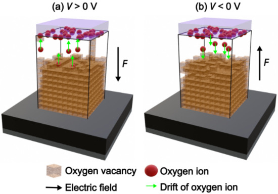
Figure 1.
(a) Deoxidation to former conductive filaments; (b) oxidation of conductive filaments.
Figure 1a shows the movement of Oions under the influence of an electric field . These ions are accumulated at the top electrode and then leave or generate VOs. These defects form complete chains of VOs or CFs that connect both electrodes. Therefore, the subsequent state of the BRSM following deoxidation is the low resistive state (LRS) or ON state. This indicates that deoxidation is essential to obtain the SET or the writing step of the BRSM. Figure 1b illustrates how a change in voltage polarization enables the return of Oions towards the oxide, enhancing the recombination or oxidation of VO, and then the interruption of CFs near the top electrode. This process, known as oxidation, effectively allows the RESET process or the erasing of the BRSM, returning the device to a high resistive state (HRS) or OFF state [30].
3. Three-Dimensional Kinetic Monte Carlo Simulation
One of the optimal approaches to simulate the behavior of c-NCs embedded in oxides is to model them as 3D clusters. The 3D coordinate system used for the simulation is shown in Figure 2.
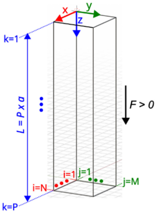
Figure 2.
Coordinate system in the oxide used for simulation.
The lattice constant of the oxide () is the level selected to simulate the distributions of VOs. The oxide is divided into sites with a thickness of . The area is selected to represent the structure of the oxide with a total area . By selecting , the computational cost of the simulation can be reduced. When a positive voltage is applied to the top electrode, the electric field is positive.
The kinetic Monte Carlo simulation employs the harmonic transition state theory or Vyneyard’s theory to calculate the generation and recombination probabilities of VOs. This theory streamlines the molecular dynamic simulation of Oions, assuming harmonic oscillation modes at the shallow and deep levels of potential wells. Therefore, the statistical physics of these vibrations is represented by an effective frequency of harmonic transition state theory or escape frequency () with a value Hz [31,32,33].
The generation probability () is calculated using Arrhenius’s relation, Equation (1). The Oion accumulates potential energy during a time ; subsequently, they could escape from the site , generating a new VO [20].
Regarding the recombination probability of VO, i.e., the RESET process, the oxidation depends on the speed of Oions. Based on the rigid ion-point model of [34], the velocity of Oions is calculated by
The thermal resistance of the CFs, , is assumed to be a constant value. The recombination probability between the Oions and VOs in the site is modeled in accordance with the methodology set forth by [20]
It is important to note that the Joule heating is concentrated in the CFs, which must be considered during their shortening [36]. Therefore, affects the temperature for the calculation of and .
Figure 3a shows the algorithm for each mesh site in consideration of the stochastic process of RS phenomena. The generation and recombination probabilities are calculated using Equations (1) and (5), respectively. These values are then compared with a random value (), where the site can change to VO or non-VO depending on its initial state. Figure 3b illustrates the flow chart for each value of voltage sweep. By using , , and , the 3D-VOC, or distribution of VO, can be calculated. The estimation of the resistive state to simulate is explained in the next section.
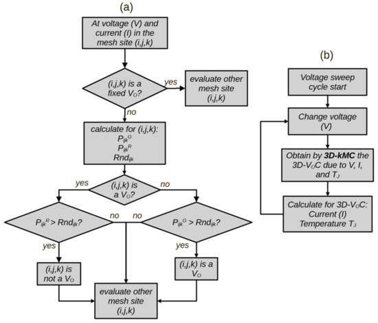
Figure 3.
(a) Algorithm for each site to implement the stochastic process using a random value. This way corresponds to the Monte Carlo method; (b) flow chart for each value of voltage sweep.
4. The Resistive State and the Simulation of the Electrical Current
It has been reported that experimental results exhibit different charge conduction mechanisms during the ON and OFF states, which are crucial insights for RS studies [37]. Based on the Mott hopping rate model, which is used to calculate the charge transport through traps, we propose to estimate the contribution of each column to the conductivity of oxide by the expression [20,38]
The charge conduction mechanism (current density in function of ) in BRSMs depends on the material used for the electrodes as well as on the active layer [37]. Our proposal is to consider different charge conduction mechanisms at the OFF and ON states. This is based on the pre-factors and , which are shown in the piecewise functions in Figure 4 [9]. The state represents the FRESH state of the BRSM, while the state indicates the OFF or HRS, while the state is the ON or LRS.
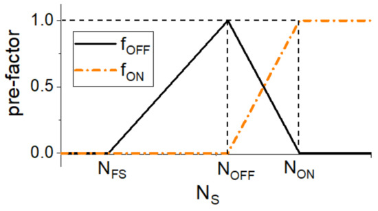
Figure 4.
Pre-factors proposed to consider different charge conduction mechanisms in the BRSM depending on the state .
Some experimental studies about RS have reported the Poole–Frenkel (P-F) conduction mechanism during the OFF state and the space-charge-limited current (SCLC) conduction mechanism in the ON state [3,37]. The P-F density current is modeled as follows [39]:
The constant is given by the formula , where is the dielectric permittivity of the oxide, is the depth of conduction traps, and depends on the effective density of states and the mobility of the conduction charge. The SCLC, including the Frenkel effect due to a high electrical field, is [40]
The temperature used for this calculation corresponds to the Joule heating, , through the CFs. depends on the effective density of states, the mobility of the conduction charge, and the density of the traps. For simplicity, the values and are assumed to be constant to be adjusted based on the experimental results.
The proposed method for calculating the electrical current is as follows:
This expression can be adapted to other conduction mechanisms distinct from P-F or SCLC.
It is a standard practice to use a limit of the electrical current to maximum values when measuring the electrical properties of RSM. This current compliance (CC) prevents the irreversible dielectric breakdown of the oxide. In our previous semi-empirical work about the 2D kinetic Monte Carlo simulation of a BRSM, we used an algorithm to emulate the CC by reducing the time (Equations (1) and (5)) at electrical currents greater than the experimental CC [9]. In the present work we have used the same algorithm.
5. Simulation and Results
To simulate the bipolar switching through c-NCs, we proposed emulating these nanostructures using clusters of fixed oxygen vacancies (f-VOs), which are VOs that cannot recombine with Oions. With the objective of evaluating the effects of c-NCs using the mathematical expressions explained above, we simulated the BRSM assuming the properties of a ZnO film as the active layer. The values used for the simulations are specified in Table 1.

Table 1.
Values used for simulations.
Figure 5a,d illustrate the structures used to simulate 3D-CVO without and with c-NCs, respectively. During the ON state, as illustrated in Figure 5b,e, the primary effect of c-NCs is the reduction in CFs, i.e., the preferential formation of VO chains through the c-NC as compared to other vertical columns where the c-NC is not present. The deoxidation–oxidation model, which forms the basis of this work, suggests that the cluster of f-VO enables the reduction in the equivalent distance between the electrodes, as indicated in (2). Figure 5c,f demonstrates how the RESET process produces these OFF states through the recombination of VOs near the top electrode.
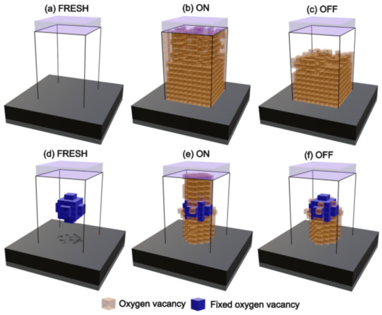
Figure 5.
Simulation of 3D-CVO for the BRSM without c-NCs (a) at FRESH, (b) ON, and (c) OFF states, and for the BRSM with c-NCs (d) at FRESH, (e) ON, and (f) OFF states.
Figure 6a shows the simulation of through five voltage sweeps: (1) FORMING of the first CFs, (2) ON state during the return to V at positive voltage, (3) erase or RESET process, (4) OFF state during the return to V at negative voltage, and (5) write or SET process. As we can see, both BRSMs with and without a c-NC exhibit three distinct stable states near to , , and (Table 1). Furthermore, the simulation results demonstrate the closed-loop functionality of the BRSM, encompassing the SET and RESET processes. Initially, during sweep 1 before the FORMING, the BRSMs with c-NCs have a stable state greater than BRSMs without c-NCs. This effect can be explained because the conductivity of the cluster of f-VO reduces the resistivity of the active layer of ZnO, as compared to the BRSM without the c-NC. On the other hand, the c-NC enables the possibility of the FORMING of first CFs at a lower voltage and . The simulation of the RESET process produces the recombination of VO, which is located in the top middle of the oxide as illustrated in Figure 5c,d. Therefore, the state during the OFF state for both BRSMs is similar, as shown in Figure 6a.
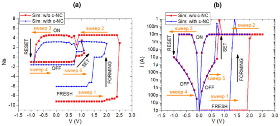
Figure 6.
Simulation of BRSMs without and with c-NCs: (a) and (b) . The voltage sweep 1 from 0.0 V to 2.5 V for BRSMs without c-NCs and 0.0 V to 2.0 V with c-NCs. The voltage sweep 2 from 2.5 V to 0.0 V for BRSMs without c-NCs and 2.0 V to 0.0 V with c-NCs. The voltage sweep 3 from 0.0 V to −1.0 V for both BRSMs. The voltage sweep 4 from −1.0 V to 0.0 V for both BRSMs. The voltage sweep 5 from 0.0 V to 1.1 V for both BRSMs.
As observed in Figure 6b, the simulation of the electrical behavior of both BRSMs presents the closed loop of current–voltage (I–V) curves similar to experimental I-V results of devices based in binary metal oxides or semiconductor oxides like TiO2, ZnO, NiO, WO3, HfO2, or SiOx [7,41]. It is evident that the presence of c-NCs embedded in the active layer reduces the voltage required to obtain the FORMING and SET processes thanks to the presence of a lower quantity of complete CFs that change the BRSM from the OFF to ON states with respect to the BRSM without c-NCs. Moreover, the nonhomogeneous electric field, modeled in Equation (2), in the vertical columns where the c-NCs are located is greater at the same voltage levels with respect to the BRSM without c-NCs. These results of simulation are according to the explanation of previous experimental results when nanostructures are included in the oxide matrix of RSMs [7,42,43].
6. Conclusions
The harmonic transition state theory and the rigid ion-point model are complemented with the Monte Carlo method to simulate the stochastic process of generation–recombination of VOs in BRSMs based on the deoxidation–oxidation mechanism. Our approach to the resistive state () through 3D-VOC allows us to take into account different charge conductive mechanisms at ON and OFF states. The emulation of c-NCs as bulk f-VO clusters embedded in oxides helps to take account of these nanostructures in the 3D-kMC to simulate BRS phenomena. Thus, the oxides with c-NC-based BRSMs are an important alternative for the development of BRSMs since they allow the formation of focalized CFs through c-NCs. This results in fewer VOs reaching the ON state of the BRSM, which can decrease the defects produced for the applied electric fields and then reduce the voltage required for the FORMING and the SET processes.
Author Contributions
Conceptualization, J.R.-R. and A.M.-S.; simulations, J.R.-R. and J.J.A.-B.; writing—original draft preparation, J.R.-R., J.J.A.-B. and A.M.-S.; writing—review and editing, J.R.-R., J.J.A.-B., A.M.-S., M.M.-M. and L.H.-M.; project administration, A.M.-S.; funding acquisition, L.H.-M., M.M.-M. and A.M.-S. All authors have read and agreed to the published version of the manuscript.
Funding
This research was funded by Consejo Nacional de Humanidades, Ciencias y Tecnologías (Conahcyt) from Mexico through the research project #A1-S-8205.
Institutional Review Board Statement
Not applicable.
Informed Consent Statement
Not applicable.
Data Availability Statement
No new data were created or analyzed in this study. Data sharing is not applicable to this article.
Acknowledgments
Juan Ramirez-Rios and José Juan Avilés-Bravo received support from Conahcyt of Mexico through the PhD scholarship grant #869500 and 852431, respectively. Juan Ramirez-Rios received support from the National Institute of Astrophysics, Optics and Electronics (INAOE) for the collaboration scholarship grant.
Conflicts of Interest
The authors declare no conflicts of interest.
References
- Zahoor, F.; Zulkifli, T.Z.A.; Khanday, F.A. Resistive Random Access Memory (RRAM): An Overview of Materials, Switching Mechanism, Performance, Multilevel Cell (mlc) Storage, Modeling, and Applications. Nanoscale Res. Lett. 2020, 15, 90. [Google Scholar] [CrossRef] [PubMed]
- Lanza, M.; Wong, H.-S.P.; Pop, E.; Ielmini, D.; Strukov, D.; Regan, B.C.; Larcher, L.; Villena, M.A.; Yang, J.J.; Goux, L.; et al. Recommended Methods to Study Resistive Switching Devices. Adv. Electron. Mater. 2018, 5, 1800143. [Google Scholar] [CrossRef]
- Hu, C.; Wang, Q.; Bai, S.; Xu, M.; He, D.; Lyu, D.; Qi, J. The effect of oxygen vacancy on switching mechanism of ZnO resistive switching memory. Appl. Phys. Lett. 2017, 110, 2–5. [Google Scholar] [CrossRef]
- Carta, D.; Salaoru, I.; Khiat, A.; Regoutz, A.; Mitterbauer, C.; Harrison, N.M.; Prodromakis, T. Investigation of the Switching Mechanism in TiO2-Based RRAM: A Two-Dimensional EDX Approach. ACS Appl. Mater. Interfaces 2016, 8, 19605–19611. [Google Scholar] [CrossRef] [PubMed]
- Aldana, S.; García-Fernández, P.; Romero-Zaliz, R.; González, M.B.; Jimenez-Molinos, F.; Gómez-Campos, F.; Campabadal, F.; Roldan, J.B. Resistive switching in HfO2 based valence change memories, a comprehensive 3D kinetic Monte Carlo approach. J. Phys. D Appl. Phys. 2020, 53, 225106. [Google Scholar] [CrossRef]
- Rahmani, M.K.; Ismail, M.; Mahata, C.; Kim, S. Effect of interlayer on resistive switching properties of SnO2-based memristor for synaptic application. Results Phys. 2020, 18, 103325. [Google Scholar] [CrossRef]
- González-Flores, K.E.; Horley, P.; Cabañas-Tay, S.; Pérez-García, S.; Licea-Jiménez, L.; Palacios-Huerta, L.; Aceves-Mijares, M.; Moreno-Moreno, M.; Morales-Sánchez, A. Analysis of the conduction mechanisms responsible for multilevel bipolar resistive switching of SiO2/Si multilayer structures. Superlattices Microstruct. 2020, 137, 106347. [Google Scholar] [CrossRef]
- Kwon, S.; Kim, M.J.; Lim, D.H.; Jeong, K.; Chung, K.B. Controlling resistive switching behavior in the solution processed SiO2-x device by the insertion of TiO2 nanoparticles. Sci. Rep. 2022, 12, 8405. [Google Scholar] [CrossRef]
- Ramirez-Rios, J.; González-Flores, K.E.; Avilés-Bravo, J.J.; Pérez-García, S.A.; Flores-Méndez, J.; Moreno-Moreno, M.; Morales-Sánchez, A. Semiempirical Two-Dimensional Model of the Bipolar Resistive Switching Process in Si-NCs/SiO2 Multilayers. Nanomaterials 2023, 13, 2124. [Google Scholar] [CrossRef]
- Zidan, M.A.; Chen, A.; Indiveri, G.; Lu, W.D. Memristive computing devices and applications. J. Electroceram. 2017, 39, 4–20. [Google Scholar] [CrossRef]
- Sze, S.M.; Lee, M.K. Semiconductor Devices: Physics and Technology; John Wiley & Sons: Hoboken, NJ, USA, 2012. [Google Scholar]
- Marković, D.; Mizrahi, A.; Querlioz, D.; Grollier, J. Physics for Neuromorphic Computing. Nat. Rev. Phys. 2020, 2, 499–510. [Google Scholar] [CrossRef]
- Yin, X.B.; Tan, Z.H.; Yang, R.; Guo, X. Single crystalline SrTiO3 as memristive model system: From materials science to neurological and psychological functions. J. Electroceramics 2017, 39, 210–222. [Google Scholar] [CrossRef]
- Jo, S.H.; Chang, T.; Ebong, I.; Bhadviya, B.B.; Mazumder, P.; Lu, W. Nanoscale memristor device as synapse in neuromorphic systems. Nano Lett. 2010, 10, 1297–1301. [Google Scholar] [CrossRef] [PubMed]
- Park, S.G.; Magyari-Kope, B.; Nishi, Y. Impact of oxygen vacancy ordering on the formation of a conductive filament in TiO2 for resistive switching memory. IEEE Electron Device Lett. 2011, 32, 197–199. [Google Scholar] [CrossRef]
- Kim, S.; Kim, S.-J.; Kim, K.M.; Lee, S.R.; Chang, M.; Cho, E.; Kim, Y.-B.; Kim, C.J.; Chung, U.-I.; Yoo, I.-K. Physical electro-thermal model of resistive switching in bi-layered resistance-change memory. Sci. Rep. 2013, 3, 1680. [Google Scholar] [CrossRef]
- Larcher, L.; Padovani, A. Multiscale modeling of oxide RRAM devices for memory applications: From material properties to device performance. J. Comput. Electron. 2017, 16, 1077–1084. [Google Scholar] [CrossRef]
- Padovani, A.; Larcher, L.; Pirrotta, O.; Vandelli, L.; Bersuker, G. Microscopic modeling of HfOx RRAM operations: From forming to switching. IEEE Trans. Electron Devices 2015, 62, 1998–2006. [Google Scholar] [CrossRef]
- Chen, S. Physics-Based Stochastic Three-Dimensional Modeling for Metal–Oxide Resistive Random Access Memory. IEEE Trans. Electron Devices 2021, 68, 3353–3358. [Google Scholar] [CrossRef]
- Guan, X.; Yu, S.; Wong, H.S.P. On the switching parameter variation of metal-oxide RRAM—Part I: Physical modeling and simulation methodology. IEEE Trans. Electron Devices 2012, 59, 1172–1182. [Google Scholar] [CrossRef]
- Yu, S.; Guan, X.; Wong, H.S.P. On the switching parameter variation of metal oxide RRAM—Part II: Model corroboration and device design strategy. IEEE Trans. Electron Devices 2012, 59, 1183–1188. [Google Scholar] [CrossRef]
- Omura, Y.; Mallik, A. Simulation study on physical parameters ruling unipolar resistance switching of sputter-deposited silicon oxide film on Si substrate. Solid State Electron 2023, 206, 108670. [Google Scholar] [CrossRef]
- Chua, L. Memristor-The missing circuit element. IEEE Trans. Circuit Theory 1971, 18, 507–519. [Google Scholar] [CrossRef]
- Chae, S.C.; Lee, J.S.; Kim, S.; Lee, S.B.; Chang, S.H.; Liu, C.; Kahng, B.; Shin, H.; Kim, D.; Jung, C.U.; et al. Random Circuit Breaker Network Model for Unipolar Resistance Switching. Adv. Mater. 2008, 20, 1154–1159. [Google Scholar] [CrossRef]
- Bocquet, M.; Deleruyelle, D.; Aziza, H.; Muller, C.; Portal, J.M. Compact modeling solutions for OxRAM memories. In Proceedings of the 2013 IEEE Faible Tension Faible Consommation, FTFC 2013, Paris, France, 20–21 June 2013; pp. 2–5. [Google Scholar] [CrossRef]
- Bocquet, M.; Deleruyelle, D.; Aziza, H.; Muller, C.; Portal, J.-M.; Cabout, T.; Jalaguier, E. Robust compact model for bipolar oxide-based resistive switching memories. IEEE Trans. Electron Devices 2014, 61, 674–681. [Google Scholar] [CrossRef]
- Roldán, J.B.; González-Cordero, G.; Picos, R.; Miranda, E.; Palumbo, F.; Jiménez-Molinos, F.; Moreno, E.; Maldonado, D.; Baldomá, S.B.; Al Chawa, M.M.; et al. On the thermal models for resistive random access memory circuit simulation. Nanomaterials 2021, 11, 1261. [Google Scholar] [CrossRef]
- Ramirez, J.F.; Perez, S.A.; Moreno, M.; Morales, A. 2D simulation of the resistive state in bipolar resistive switching memories based on oxygen vacancies. In Proceedings of the 2022 IEEE Latin America Electron Devices Conference, LAEDC 2022, Cancun, Mexico, 4–6 July 2022. [Google Scholar] [CrossRef]
- Maldonado, D.; Aguilera-Pedregosa, C.; Vinuesa, G.; García, H.; Dueñas, S.; Castán, H.; Aldana, S.; González, M.; Moreno, E.; Jiménez-Molinos, F.; et al. An experimental and simulation study of the role of thermal effects on variability in TiN/Ti/HfO2/W resistive switching nonlinear devices. Chaos Solitons Fractals 2022, 160, 112247. [Google Scholar] [CrossRef]
- Yu, S.; Wong, H.S.P. A phenomenological model for the reset mechanism of metal oxide RRAM. IEEE Electron Device Lett. 2010, 31, 1455–1457. [Google Scholar] [CrossRef]
- Voter, A.F. Introduction to the Kinetic Monte Carlo Method. In Radiation Effects in Solids; Springer: Berlin/Heidelberg, Germany, 2007; pp. 1–23. [Google Scholar] [CrossRef]
- Vineyard, G.H. Frequency factors and isotope effects in solid state rate processes. J. Phys. Chem. Solids 1957, 3, 121–127. [Google Scholar] [CrossRef]
- Uberuaga, B.P.; Voter, A.F. Accelerated molecular dynamics methods. In Radiation Effects in Solids; Springer: Berlin/Heidelberg, Germany, 2007; pp. 25–43. [Google Scholar] [CrossRef]
- Strukov, D.B.; Williams, R.S. Exponential ionic drift: Fast switching and low volatility of thin-film memristors. Appl. Phys. A Mater. Sci. Process. 2009, 94, 515–519. [Google Scholar] [CrossRef]
- Russo, U.; Ielmini, D.; Cagli, C.; Lacaita, A.L. Self-accelerated thermal dissolution model for reset programming in unipolar resistive-switching memory (RRAM) devices. IEEE Trans. Electron Devices 2009, 56, 193–200. [Google Scholar] [CrossRef]
- Russo, U.; Ielmini, D.; Cagli, C.; Lacaita, A.L. Filament conduction and reset mechanism in NiO-based resistive-switching memory (RRAM) devices. IEEE Trans. Electron Devices 2009, 56, 186–192. [Google Scholar] [CrossRef]
- Lim, E.; Ismail, R. Conduction Mechanism of Valence Change Resistive Switching Memory: A Survey. Electronics 2015, 4, 586–613. [Google Scholar] [CrossRef]
- Mott, N.F.; Davis, E.A. Electronic Processes in Non-Crystalline Materials; Oxford University Press: Oxford, UK, 1979. [Google Scholar]
- Sahoo, S.K.; Misra, D. Interfacial layer growth condition dependent carrier transport mechanisms in HfO2/SiO2 gate stacks. Appl. Phys. Lett. 2012, 100, 232903. [Google Scholar] [CrossRef]
- Murgatroyd, P.N. Theory of space-charge-limited current enhanced by Frenkel effect. J. Phys. D Appl. Phys. 1970, 3, 151–156. [Google Scholar] [CrossRef]
- Patil, A.R.; Dongale, T.D.; Kamat, R.K.; Rajpure, K.Y. Binary metal oxide-based resistive switching memory devices: A status review. Mater. Today Commun. 2023, 34, 105356. [Google Scholar] [CrossRef]
- Morales-Sánchez, A.; González-Flores, K.E.; Pérez-García, S.A.; González-Torres, S.; Garrido-Fernández, B.; Hernández-Martínez, L.; Moreno-Moreno, M. Digital and Analog Resistive Switching Behavior in Si-NCs Embedded in a Si/SiO2 Multilayer Structure for Neuromorphic Systems. Nanomaterials 2023, 13, 986. [Google Scholar] [CrossRef]
- González, K.E.; Palacios-Márquez, B.; Alvarez-Quintana, J.; Pérez–García, S.A.; Licea–Jiménez, L.; Horley, P.P.; Morales-Sánchez, A.; Jiménez, L.L. Resistive switching control for conductive Si-nanocrystals embedded in Si/SiO2 multilayers. Nanotechnology 2018, 29, 395203. [Google Scholar] [CrossRef]
Disclaimer/Publisher’s Note: The statements, opinions and data contained in all publications are solely those of the individual author(s) and contributor(s) and not of MDPI and/or the editor(s). MDPI and/or the editor(s) disclaim responsibility for any injury to people or property resulting from any ideas, methods, instructions or products referred to in the content. |
© 2025 by the authors. Licensee MDPI, Basel, Switzerland. This article is an open access article distributed under the terms and conditions of the Creative Commons Attribution (CC BY) license (https://creativecommons.org/licenses/by/4.0/).