Article

A CMOS 12-Bit 3MS/s Rad-Hard Digital-to-Analog Converter Based on a High-Linearity Resistor String Poly-Matrix

RedCat Devices, 20143 Milan, Italy
*
Author to whom correspondence should be addressed.
Chips 2024, 3(2), 129-152; https://doi.org/10.3390/chips3020006
Submission received: 4 March 2024 / Revised: 8 April 2024 / Accepted: 1 May 2024 / Published: 8 May 2024

Abstract

:
This work presents a rad-hard 12-bit 3 MS/s resistor string DAC for space applications. The converter has been developed using rad-hardened techniques both at architecture and layout levels starting from a conventional topology. The design considers the different effects of the radiation that could damage the circuits in space environments. The DAC has been developed and integrated a standard CMOS 0.13 μm technology by IHP, using RHBD techniques. Low Earth Orbit (LEO) requires a TID value of around 100 krad (Si), according to the expected length of the mission. The temperature range is between −55 °C and 125 °C. The DAC power budget is similar to that of terrestrial applications. The measured INL (Integral Non-Linearity) and DNL (Differential Non-Linearity) are better than 0.2 LSB, while the ENOB (Effective Number Of Bits) at a 3 MS/s clock exceeds 9.7 bits while loading a 10 pF capacitor. The DAC has been characterized under radiation, showing a fluctuation in the analog output lower than 2 LSB (mainly due to measurement uncertainty) up to 500 krad (Si). Power consumption shows a negligible increase, too. A 10-bit version of the same DAC as the downscaled 12-bit one has been developed as well.

1. Introduction

In a continuously evolving scenario thanks to new silicon processes and more demanding requirements coming from the space community, DACs and ADCs help moving functions belonging to the analog world towards the more consolidated digital domain, thus leading to an evident expansion of complex mixed-signal ICs. Currently, DAC (and Analog-to-Digital Converter) performance is often a bottleneck for practical applications because of the non-idealities they introduce, such as poor accuracy, speed limitations, distortions, etc. In a consolidated standard consumer market, many high-speed DACs are commercially available, in particular for video applications or wired and wireless communications, leveraging a variety of modulation and encoding (and sometimes quite sophisticated) schemes to exchange digital information. In space applications, DACs are requested as well and represent a fundamental element either as stand-alone devices or embedded macro inside rad-hard microcontrollers. Their role is crucial for satellite housekeeping or ICs focused on propulsion control.
Space environment requires the employment of radiation-resilient components able to safely operate during the whole system’s life. Thus, in addition to usual requirements for terrestrial applications, the goal for “space” engineers is to design and manufacture high-performance radiation-tolerant or even radiation-hard DACs using standard commercial processes of integration that are inexpensive, easy to maintain, and widely available in the industry.
The main threat for space ICs is represented by high-energy particles, including heavy ions, protons, electrons, X-rays, and gamma rays, which can degrade the characteristics of the internal circuits or, in the worst cases, permanently damage their behavior. There are two main effects to be considered: Total Ionizing Dose (TID) and Single Event Effect (SEE). TID is an effect working with time and usually brings the IC to a progressive degradation coming from the hole–electron pair generation and leaving behind charge traps in critical parts of the chip (STI, Shallow Trench Isolation, and transistors’ channel); the result is a threshold voltage slightly moving with time (decreasing in N-channel and increasing in P-channel) and in the worst scenario, they may compromise their natural behavior [1,2]. It is worthless to say that a shifting threshold voltage leads to an unstable transconductance (gm) that, for analog applications, has strong impacts in terms of gain, accuracy, and stability of feedback loops.
If TID works with time, SEE is stochastic, and it arises from the impinging of energetic particles, like heavy ions, releasing energy in their passage along active area regions (N-doped or P-doped). In the case of protons, the primary energy release can be the result of secondary particles (e.g., alpha particles) generated by spallation when colliding with specific elements in the chip (e.g., boron in the passivation). SEE, essentially, provides a strong hole–electron pair generation that, in the transistors’ channel, is translated in a drift current (during the hole–electron separation) and diffusion current (during the recombination); both contribute to generating a current spike that, at the circuit level, is seen as voltage spike or, more simply, as a Single Event Transient (SET). SETs affect all active components and for sequential cells (flip flop or latches), they can even change the bit content; in this case, the SET changes its name in SEUs (Single Event Upsets).
SETs and SEUs are typical soft errors but when the energy release is very high, vertical and lateral bipolar transistors (intrinsic in every CMOS technology) can become the source of radiation-induced latch-up, also called Single Event Latch-ups (SELs), which is the main hard error to be considered when designing a space-grade IC.
In this work, the aim has been to develop a rad-hard DAC featuring 12 bits and running at a maximum frequency of 3 MS/s with a target of 300 krad (Si) in terms of TID. The developed DAC prototypes have been characterized using an improved version of the testing methodology under ionizing radiation already used for SRAM [3] and ADC [4]. A 10-bit version of the same DAC downscaled from the 12-bit one has been developed as well [5], as demonstrated by the modularity of the design.
The following section illustrates the state-of-the-art and main approaches to implementing a rad-hard Digital-to-Analog converter. Then, the proposed 12-bit DAC architecture and design countermeasures taken to make it radiation hard are presented. In this section, we discuss the relevant points of the layout style, which has an impact on the resiliency to ionizing radiation, too. Finally, in Section 4, test results both in the lab environment and under radiation are shown.

2. Rad-Hard Digital-to-Analog Converters

In the literature, there are several DAC architectures, each addressing different resolution speed requirements. Among the most popular are the following:
  • Type 1—resistive (resistors, switches, and logic ports);
  • Type 2—capacitive (capacitors, switches, and logic ports);
  • Type 3—current steering (current generators, switches, and logic ports).
Other topologies, such as sigma–delta based [6,7], address more specific applications and performance ranges. Indeed, sigma–delta are less “general purpose” and address more specific applications and performance ranges (namely, they operate on a very-low-frequency bandwidth. Ref. [6] showed a signal bandwidth of 0.1 mHz–50 kHz, while Ref. [7] showed a signal bandwidth of 0.1 mHz–1 kHz. From the electrical point of view, Type 1 is based on the principle of a resistive divider (also called a Kelvin divider). It is simple and monotonic but has several control lines, a high parasitic load at a buffer input and is very variable with code (because of the large number of switches), and poor matching for high bit counts. Type 2 is based on the so-called charge-sharing technique, and its performance is strongly related to the capacitor mismatch. Type 3 is suitable for very high speeds, but differential (and consequently integral) non-linearity is strongly dependent on the matching of the binary-weighted currents, so suitable averaging techniques are mandatory, especially under radiations.
All these architectures shall be assessed with respect to radiation since they exhibit a different behavior as a response. Current-steering DACs are very sensitive to the total dose and have their accuracy based on matching between MOS and current generators (both unary and binary weighted), and even a little gradient in the variation in the threshold voltages can degrade linearity. On the other side, capacitive DACs being made up of capacitors (generally MIM, Metal–Insulator–Metal) and switches are subject to the hit of high-energy particles, which can alter the charge “content” of the array. The high-energy particle definition for SELs is canonically fixed at 60 MeV × cm2/mg, while for SEUs, it is 10 MeV × cm2/mg.
Resistive DACs represent the best compromise. Indeed, DAC resistors in polysilicon are essentially insensitive to radiation, while switches suffer from leakage currents induced by TID and mitigated by a MOS length greater than the minimum and ELT (Edge-Less Transistor) shapes. In case of a high-energy event, a transient glitch can be observed at the DAC output, but it subsides with the time constant of the DAC (usually a time of a few nanoseconds) and is reabsorbed, so it must be assessed on a case-by-case basis whether it disturbs. TID and SEE issues for DAC digital circuits are similar to those typical of generic digital circuits. For example, the robust design of sequential cells or TMR (triple modular redundancy) is a typical technique to overcome them. The summary of rad-hard performances of a typical DAC analog core and the adopted provisions to make it resilient can be found in Table 1 [5].
The meaning of the last three rows is that there are design levels where the effort to make the DAC resilient is lower or higher (the lower the better). As already mentioned, the key point of resistive architectures is that they allow us to employ silicide polysilicon as a material, which has been demonstrated to be insensitive to the dose [8,9].
For commercial DACs, several tests have been performed in the past on off-the-shelf components, showing to which extent TID and SEE can affect device performance [10,11,12,13,14]. It is worth noting that the main part of commercial components is radiation tolerant or radiation hard up to some tens of krad (Si). Generally, they are based on some kind of resistive architecture, confirming the goodness of such an approach.
Also, the world of academia started to work on this topic to study solutions to rad-hard DAC issues. Some significant examples of a radiation “tolerant” DAC exist at the research stage [15,16,17,18,19,20]. A few of them will be briefly described below; the first two are based on resistors, while the others are based on current steering. To the authors’ knowledge, there are no examples of research ongoing on a capacitor-based rad-hard DAC.

2.1. Resistor String Rad-Hard DACs in the Literature

Starting from the conventional resistor-based Digital-to-Analog converters, different techniques have been applied to the circuital, layout, and process levels to make them resilient to the dose. The DAC proposed in Ref. [15] presents the implementation of a four-channel 12-bit DAC with high-voltage operation that is radiation tolerant in a 0.5 μm Bi-CMOS technology to achieve the functionality at a high voltage (±15 V) and across a wide temperature range (−55 °C to 125 °C). The canonical R-2R ladder resistor networks are adopted as the starting point to provide necessary resistor matching. Any additional digital calibrations or laser trimmings are needed to obtain a resolution. The resistor network is decoupled from the output by means of an inverting buffer. The DAC can satisfy the circuit specifications for low orbit satellite (LEO) applications to fully support a total ionizing dose of 10 krad (Si)with minimum degradation up to 20 krad (Si).
In this work, an unconventional layout technique considers not only the matching between the MSB (Most Significant Bit) and LSB (Less Significant Bit) resistors but also the matching between LSB resistors, significantly improving the DAC precision and linearity. The resistors of the R-2R ladder are split into a different number of resistors of the same size, which can minimize the mismatches between devices and the relevant parasitic resistance and capacitance. The common centroid layout is not only adopted globally in the whole array but also every local region so that the resistor mismatch caused by stress and temperature gradients is greatly reduced. Moreover, the connections between the entire resistive arrays are realized everywhere with the same metal without vias and multi-layer interconnections so that the system mismatch caused by them is significantly decreased.
For radiations, high-precision polysilicon resistors are chosen since they can meet the requirements of both high-voltage operations and insensitivity to the total dose. In this design, the analog block adopts a high-voltage (HV, ±15 V) design, and the digital block contains both high-voltage and low-voltage designs. In the analog block, the length of the HV MOS transistors is larger than the minimum, which can ensure single event tolerance of the device. Moreover, the tolerance to inter-device leakage is improved by means of guard rings, such as a triple ring of N+, P+, and N-well isolate PMOS and a double ring of P+ and N-well isolate NMOS.
For this DAC, the authors have introduced triple modular redundancy (TMR) to improve the resiliency to single event upsets (SEUs), with penalties in terms of area and speed. For this reason, they have used TMR only in crucial sub-blocks.
Given that electrical performances are those typical of this class of circuits (DNL and INL are <1 LSB in all temperature cases), the behavior of the output voltage under a total dose of 60Co is optimum until 10 krad (Si) and it starts to degrade around 20 krad (Si). This value is suitable for LEO but too low for longer missions.
One more rad-hard R-2R DAC is described in Ref. [16]. It has been implemented in a 0.5 um SiGe BiCMOS technology, which features wide temperature capabilities and high speeds. A segmented R-2R ladder architecture has been selected for its simplicity, low power, and less active component use. It features eight bits segmented in five binary LSBs and three MSBs with thermometer codes. The reference current generator is implemented with an accurate MOS cascode current mirror starting from an ultra-wide-temperature bandgap reference. In order to make the generators resilient, an MOS length higher than the minimum lithographic length has been used, while RHBD provisions have been taken against SEL. Active N+ (P+) guard rings are added around pMOS (nMOS); N-well and P-substrate contacts are widely used; deep trench rings are added for isolation between pMOS and nMOS; and N-well and n+ source/drain are kept as farther away as possible. The measured DNL/INL at room temperature is well below ±0.5 LSB, while the variability over −120 °C to 180 °C is less than ±1 LSB. Unfortunately, any measurements under radiation are given in Ref. [17], which adopts quite similar architecture.

2.2. Current-Steering Rad-Hard DACs in the Literature

A first example of a rad-hard current-steering DAC can be found in [18]. Here, in addition to general electrical requirements (a resolution of 12 bits and a data rate of 80 MS/s), the device shall satisfy radiation tolerance and operation over a cryogenic temperature range (−180 °C to 120 °C) required for lunar applications. The technology used is a 0.5 um BiCMOS SiGe, which is an expensive and not common process but guarantees immunity to radiation for SiGe bipolar devices.
This current-steering DAC is implemented with a segmented architecture and is made up of three sections: 6 MSB + 4 NSB + 2 LSB (NSBs; Next Most Significant Bits). The blocks that make up the DAC are the following: a segmented current source array with a related current switch logic array, a thermometer decoder, a clock driver, and a bias generator based on a bandgap voltage reference. Partial segmentation for the MSBs is combined with a binary weighting for the LSBs, thus achieving a satisfactory trade-off between circuit complexity and good accuracy and dynamic performance. After a deep analysis, the optimal segmentation has been 6 MSB + 4 NSB + 2 LSB, which results in the best balancing between reduced circuit area for thermometer decoders and static and dynamic performance.
While the switches and relevant control circuits have a conventional topology, the bandgap has been designed to support a wide temperature range (−180 °C to +120 °C). The bandgap utilizes unique SiGe bipolar transistors to generate temperature-independent voltage sources.
For radiation tolerance, the focus of the design has been on the total dose, which limits the operation lifetime. Indeed, the total dose changes the threshold voltage of MOS transistors. In current-steering DACs, the output currents are the results of the summation of the precise unit current sources. Since the ionizing radiation can induce a consistent inaccuracy in the unit current cells (by modifying the transistor threshold voltage), the DAC static and dynamic performance, such as the SFDR (Spurious Free Dynamic Range) and ENOB (Effective Number of Bit), are significantly degraded. The provision taken was to use large W/L transistors, which can partially mitigate the threshold shift and cumulative charge. Moreover, as said above, the bandgap is built up with SiGe bipolar transistors available in the technology, which are insensitive to the dose and offer wide temperature capabilities. Also, the layout has been carefully performed using dummy transistors and a large area to improve resiliency to the dose. Moreover, extended guard rings are used to provide isolation between current sources and reduce inter-device leakages.
Several measurements are reported in this paper. The output current varies by around 100 ppm/°C over the temperature range, confirming the validity of the designed bandgap. The measured SFDR at a reduced clock rate (25 MS/s) is −54 dBc at −180 °C, while its degradation at 300 krad (Si) is only 2 dB. This demonstrates that the distortion coming from the inaccuracy of unit current sources caused by total dose is modest. Power consumption at room temperature, exhibits an increase of >15% after exposure up to 300 krad (Si). These results make this DAC suitable for radiation-tolerant applications.
A second version of a rad-hard current-steering DAC is presented in [19]. In this work, the 12-bit DAC is built up with 212 unit current cells, and the authors analyze the mismatch induced in current cells by a total dose (using the Gaussian distribution for threshold variations). Using radiation parameters taken from the literature and a 65 nm CMOS technology, the evaluated degradation in the SNR (Signal to Noise Ratio) is from 74 dB (ideal case) to 41.3 dB after a 100 Mrad (Si) dose. To overcome this limitation, a technique that minimizes the mismatch between the unit current cells because of radiation on the threshold voltage VT is proposed It is accomplished by adjusting the body voltage of the current source transistor. During calibration, a simple VT extractor plus an ADC is used to read threshold voltage shifts and apply a correction to the body voltage of MOS transistors in each unit current cell by means of a resistive DAC embedded in the cell itself. This allows for the recovery of almost all degradations in the SNR.
Since the same calibration circuitry is used for minimizing the mismatch of all unit current cells, its degradation due to radiation does not have an impact. The technique has been verified by mixed simulation in Spectre® and Matlab®, demonstrating that calibration can recover up to 13 dB in the SNR after a 100 Mrad (Si) dose. Even if the proposed technique is interesting, this paper presents only a theoretical analysis, and any silicon-proven measurements are provided at a high TID (100 Mrad (Si)).
Finally, a third current-steering DAC has been presented in [20]. The DAC is integrated into a 130 nm CMOS technology and features 10 bits with a measured ENOB of 8.73 bits. However, further details are not provided in the paper.
Now, the next paragraph will describe the resistive matrix DAC proposed in this work.

3. 3 MS/S 12-Bit Poly-Resistor Rad-Hard DAC

To develop such resilient components, generally, three main approaches have been considered: process enhancement, such as SOI/SOS (Silicon on Insulator or Silicon On Sapphire), called the Radiation Hardening-By-Process, RHBP [21], shielded packages, and finally, design enhancement (Radiation Hardening-By-Design, RHBD [22]). The RHBP approach is more expensive since a special integration process shall be employed, and it shall be maintained for the lifetime of the designed component. On the other side, it allows an optimization of radiation performance without adopting any special design technique. The RHBD methodology allows us to use a standard bulk CMOS process, which has advantages in terms of cost (cheaper), low maintenance cost, and portability. These advantages are obtained at the expense of a larger occupied area due to the RHBD techniques adopted. While RHBP and shielded packages have been already employed for the development of commercial rad-hard analog components, analog RHBD has not yet been extensively applied, and it is mainly confined to the area of high-energy physics experiments [23].
Starting from a known approach to design DAC resistor-based architecture, the resiliency to radiation is obtained only by applying RHBD techniques. The proposed DAC has been integrated into a standard 0.13 μm CMOS, which guarantees good rad-hard performance while allowing a compact mixed-signal circuits design. This technology includes both 1.8 V and 3.3 V MOS; the former has thin oxide and the latter has thick oxide (used for the DAC). The DAC power supply is 3.3 V, but its operations extend up to 3.3 V + 10% (absolute max rating 3.9 V). The goal performance of the integrated DAC is a total dose immunity up to 300 krad (Si), resiliency to latch-up up to 60 MeV × mg/cm2, and an SEU of 10 MeV × mg/cm2 for the digital control section. The temperature range is −55 °C +125 °C. We have chosen a technology that is relatively mature and has a moderate length scaling since more scaled CMOS processes (such as 90 nm with a reduced gate oxide thickness) seem to be more TID “tolerant”; however, they are more prone to both SEUs and SELs. Indeed, this is due to shorter channels and reduced critical charges for SETs/SEUs.

3.1. Starting Architectures

The approach used to design a resistive DAC is to create in some way 2N reference voltages employing resistors as the basic element. According to the digital input code, one of these voltage taps is selected as the analog output signal.
In principle, this type of DAC is implemented with a string of 2N resistors biased by Vref, which divides the reference voltage into 2N voltage values (Figure 1). A network of switches, driven by the digital input code b0-b2 (and bn0-bn2), allows us to select the corresponding voltage value and to feed to the output or input terminal of a decoupling buffer. In the latter case, the buffer output terminal will be the DAC output terminal. In CMOS technology, generally, a complementary switch is used, which is a switch formed by an nMOS and a pMOS. This represents the simplest way to realize a resistor string DAC.
The monotonicity of this DAC is guaranteed because any tap of the resistor string has a lower voltage than its upper neighbor taps. The accuracy depends on the matching of the resistors and the material they are made of. However, with the increase in the number of bits, the number of resistors, switches, and control lines becomes too large. Moreover, the parasitic load at the buffer input increases and is very variable with the code. A further limitation of this circuit is speed, as the resistor string and the switches introduce a time constant and thus delay the conversion process.
To reduce the capacitance load, it is possible to use a matrix topology called a folded resistor string (or X-Y addressing scheme). An example of the 4-bit resistor string is shown in Figure 2. This solution is also used to reduce the decoder size and the control line number.
The sixteen resistors (for four bits) are divided into four lines and arranged with a serpentine shape connected between Vref+ and Vref−. Each line is selected by one of the decoded MSBs of the input code. Yi is the output of a decoder that converts the LSBs of the input code, and Xi is the output of a decoder that converts the MSBs of the input code. The most significant bits select a column of the matrix. That is, a block of adjacent resistors is connected to switches controlled by less significant bits. One of these resistors is connected to the buffer by closing a further switch. The voltage at the terminals of each resistance is a fraction of the reference voltage (VRP-VRN), so the output voltage of the DAC is one of these voltages. VRP and VRN are chosen to be compatible with the input dynamic range of the output buffer, and in any case, VRP is lower than the supply and VRN is higher than the common ground reference. The difference between VRP and VRN determines the maximum output range of the converter in terms of peak-to-peak voltage (Vpp or Vpeak-to-peak). Since there are 2N resistances, 2N voltage values are produced. You need to have a switch for each voltage value obtained, and since there are 2N voltage values, you have the number of transistors being 2(2N)/2. The factor of two derives from the fact that each switch is complementary. The factor of 1/2 results from the fact that only half of transistors relate to the output. Therefore, the number of transistors connected to the buffer is 2N [24]. Switches can be implemented as complementary MOS (nMOS and pMOS) or single MOS, depending on the chosen VRP-VRN range. Its size is always a compromise between maintaining a low on-resistance, Ron, and low parasitic capacitances. A limit of the resistive divider DAC (in all its variants) is that the number of resistors increases exponentially with the number of bits.
Starting from the consideration that the resistive string solution seems the most promising in terms of simplicity, consumption, and resiliency, the authors developed and verified a 3 MS/s DAC with 12 bit as the embedded interface in microcontrollers. Our target architecture has been the so-called “X-Y addressing scheme with shunt resistor” or “intermeshed architecture” [5,25], which is an improved variant of the folded resistor string discussed previously. The simplified schematic, including X-Y selection switches, is shown in Figure 3.
The coarse interval of voltages is defined by the main resistor string (RCx), while the sub-strings (RFy), placed in parallel to the coarse interval, define the taps for the fine voltages. RCx is selected with switches driven by 6-MSB, while RFx are selected by means of switches driven by 6-LSB. In this design, all resistors are the same size.
This architecture offers the following advantages with respect to the conventional Kelvin divider:
  • The number of bits in the control lines is reduced;
  • It is possible to keep low the time constant of the resistor matrix without using low-value unity resistors.
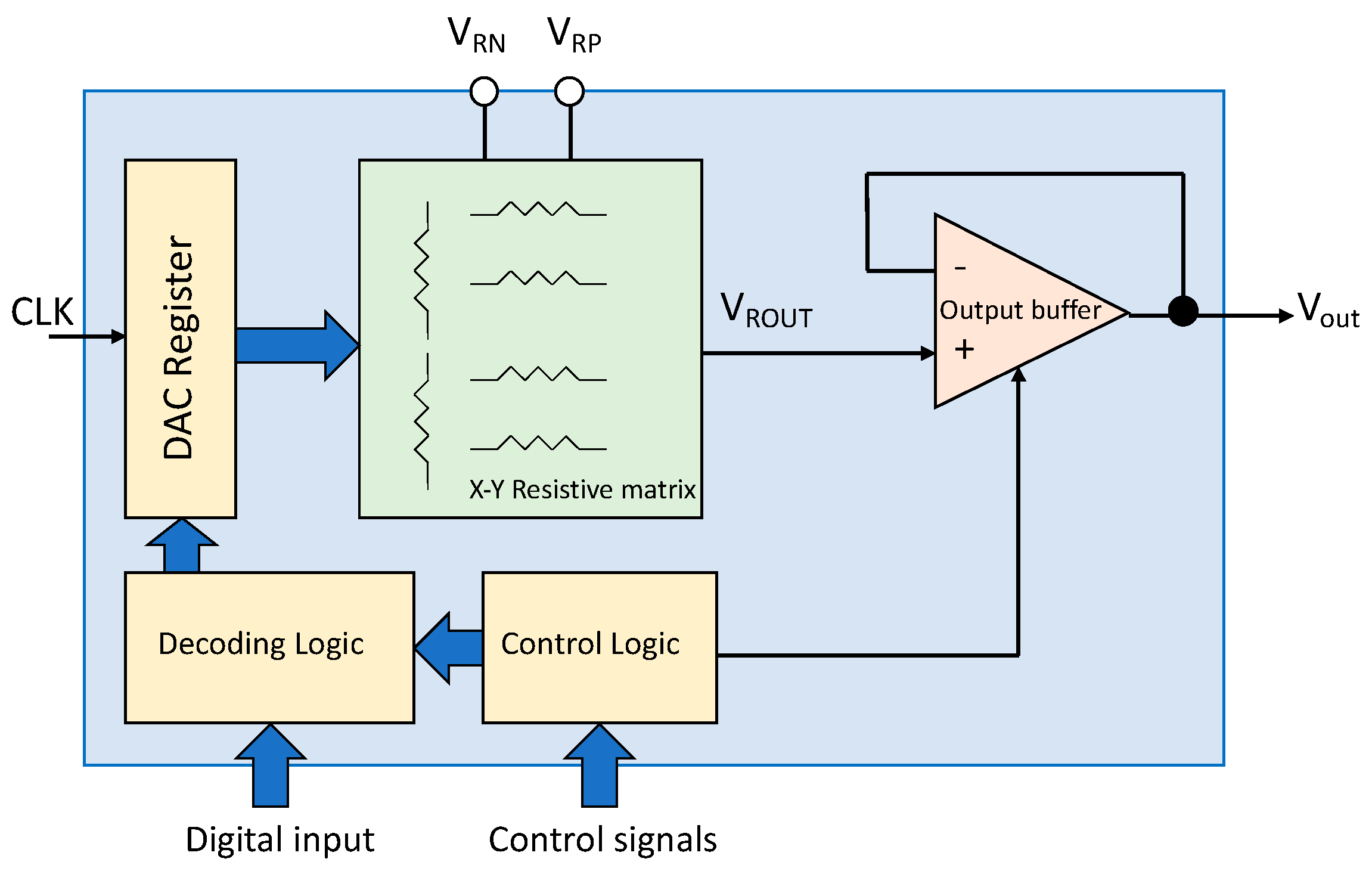
Having resistors with not too much of a low value is important since the string consumes less power. The current across them is VRP-VRN/RTOT, where RTOT is the total resistance seen between references. Moreover, thanks to this topology, resistors with a suitable value that does not degrade matching can be used. Indeed, the higher the perimeter and the area of the poly-resistor, the better the matching, so the linearity performance of the matrix (and so of the DAC) related to it is improved. Decoders, control logic, and an output buffer able to drive up to 10 pF load have been designed to complete DAC functionalities. A block diagram is shown in Figure 4, where different colors correspond to digital, analog, and matrix sections, each of them with specific rad-hard provisions.
The input 12-bit code is transformed into the X-Y address of the matrix by suitable X (for RCx) and Y (for RFy) decoders. In turn, the X-Y address selects the proper voltage tap that gives the analog voltage corresponding to the given input bit code (such as the selection of a box in a chessboard). Input bits are synchronized by suitable registers, while a control logic supervises DAC operations and realizes the Reset and Hold functions. A closed-loop unity gain buffer decouples the output load from the resistor matrix, thus improving speed performance.

3.2. Design Strategy

The sizing of the unit resistor is one of the most critical activities in the matrix design. As mentioned above, its size, area, and physical characteristics have an impact on DAC performance. After selecting the best matrix topology, resistor material is the next crucial choice. In order of priority, adopted criteria are as follows:
  • Resistor matching data;
  • Resistor value;
  • Radiation resiliency.
Resistors based on “active” layers are discarded because of their sensitivity to charges (hole–electron pair generation in the active region). In the literature, resistors based on polysilicon layers have been demonstrated to be insensitive against radiation [8] and are verified in the ADC presented in [26]. Three kinds of polysilicon resistors were available in the process.
  • Rhigh (high-ohmic poly-Si resistor);
  • Rppd (medium-resistance poly-Si resistor);
  • Rsil (salicided poly-Si resistor).
The sheet resistance of the available resistors is 1300, 250, and 7 Ohm/square, respectively, in the typical case. Extensive statistical simulations (Monte Carlo, MC) for mismatch and process variations suggested that Rsil performs the best matching behavior. Figure 5 shows an example of Monte Carlo analysis (1000 runs) performed on the matrix mid-code voltage, which is the one more affected by mismatches. The achieved Gaussian mean value is 1.64986 V (ideal = 1.6467 V), while the variance is 274 uV, which is comparable with LSBs (366 uV for a 1.5 Vpp output range).
Several trials have been performed for unit resistor sizing using statistical Monte Carlo outcomes and spectral analysis. Matching is strongly dependent on the resistor area (W × L) and weakly dependent on the perimeter (2 × (L + W)). As a “rule of thumbs”, W shall be from three to ten times the minimum lithographic, and L shall be from five to ten squares (W is the resistor width and L is the resistor length). Moreover, the value of resistors shall be performed in a small way to improve the array time constant, which for five coarse unity resistors RU is approximately given by the following:
tDAC = (26/2 × RU + 2 × Ron) × (Cp + CL)
where Ron is the switches’ on-resistance, Cp is the switches’ parasitic capacitance, and CL is the load capacitance of the resistor matrix, i.e., the input buffer capacitance. However, power consumption is proportional to 1/RTOT, so the resistor value cannot be too low.
Comparing area occupation (critical parameter), statistical performance (critical parameter), power consumption, and linearity resulted in RCx = RFy = 61 ohm. The matrix is composed of 26 RCx resistors and 26 fine strings, each of them implemented with 26 RFx. The obtained current consumption of the poly-matrix is 410 uA in typ, 350 uA in min, and 465 uA in max process corners.
For Rsil temperature dependance, in the range of −50° to 125°, the resistor absolute value varies around ±25%. However, we think that the difference between resistor temperature in the different matrix portions is not significant since there is no hot spot of power. The current flowing across the string is equal for all resistors.
Some opposite “rules of thumbs” have been followed for the sizing of switches as well.
  • Switches on-resistance shall be kept low (i.e., a W/L ratio higher than the minimum) for increasing speed;
  • Switches’ size (W and L) shall be small for a reduced parasitic capacitance;
  • Length L shall be higher than the minimum lithographic, or an ELT shape shall be adopted [23] to improve resiliency.
A complementary MOS pair (pMOS and nMOS) makes switches on-resistance more constant vs. source/drain voltages, thus mitigating non-linearity in Ron and the network time constant. The use of complementary MOS switches helps with clock feedthrough reduction, as well. The time constant of the matrix is proportional to both switches on-resistance and parasitic capacitance. A larger switch has a lower on-resistance (which is proportional to L/W) and a higher area and of parasitic capacitance; thus, a compromise has been found.
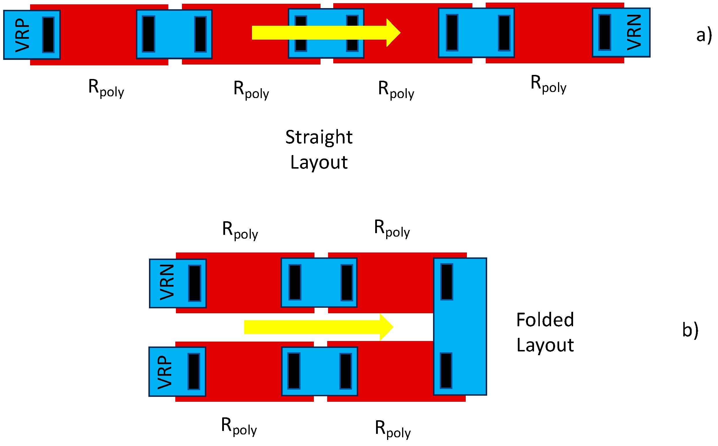
The layout of the resistor matrix plays an important role in determining DAC performance. Indeed, the resistance of a real implementation differs from the nominal value, RU, because of processing effects. In particular, the resistor is affected by an absolute error and a relative mismatch, usually with a gradient in one direction. Let us consider, for example, a straight string with unity elements RU. It can be calculated that the resistor INL has a parabolic shape. If the resistive divider is folded around its mid-point, the maximum INL is reduced by a factor of four [27] (in Figure 6 there is an example with four resistors).
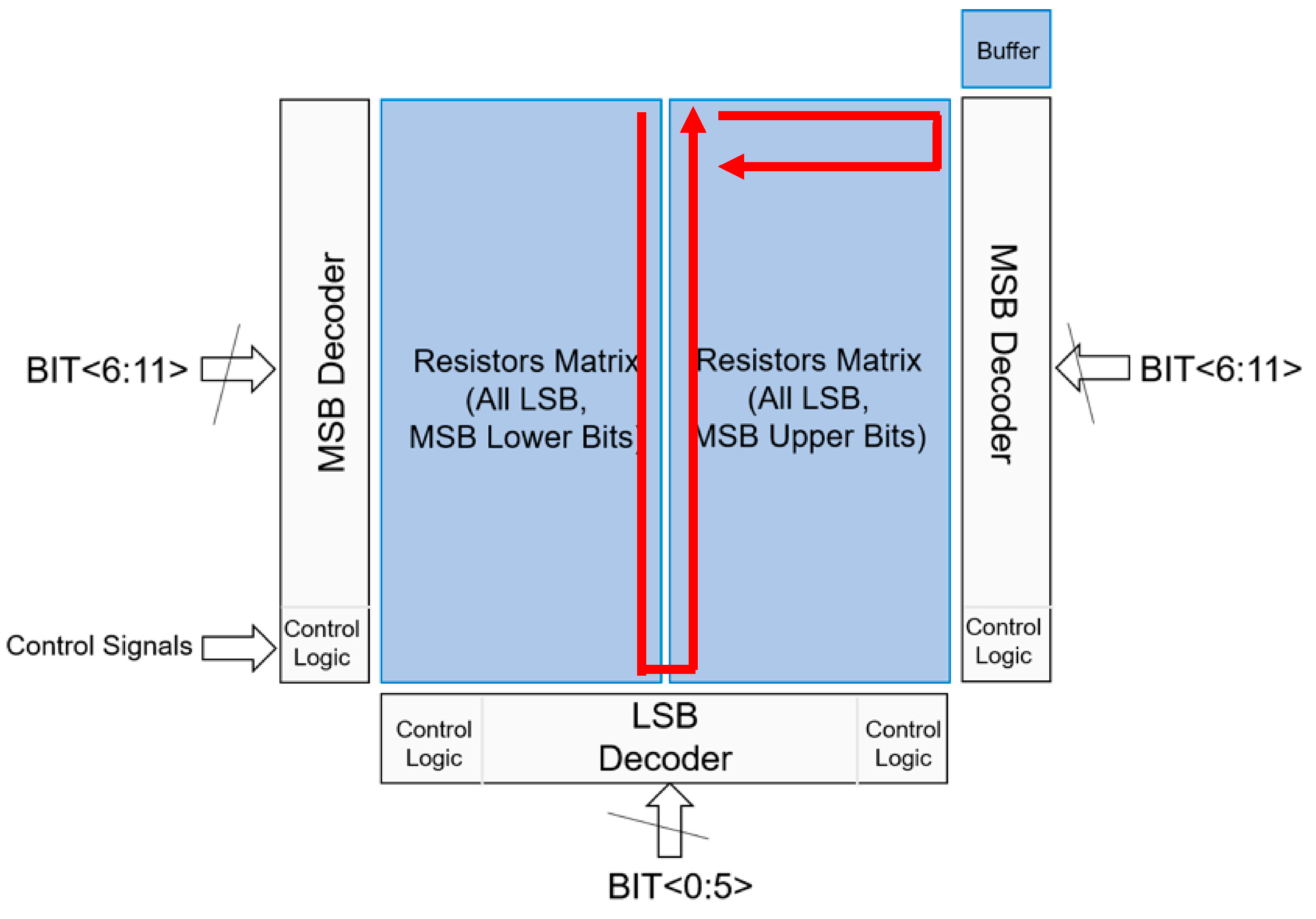
We followed the folding principle by making the layout of a matrix where rows from 1 to 26/2 are placed in the left matrix and rows from 26/2 + 1 to 26 are placed in the right matrix. Moreover, having a resistive matrix layout with a similar length and width is convenient with respect to gradient processing (Figure 7). Red arrows indicate the direction of folding for coarse and fine resistor strings. In addition, fine resistors are intermeshed.
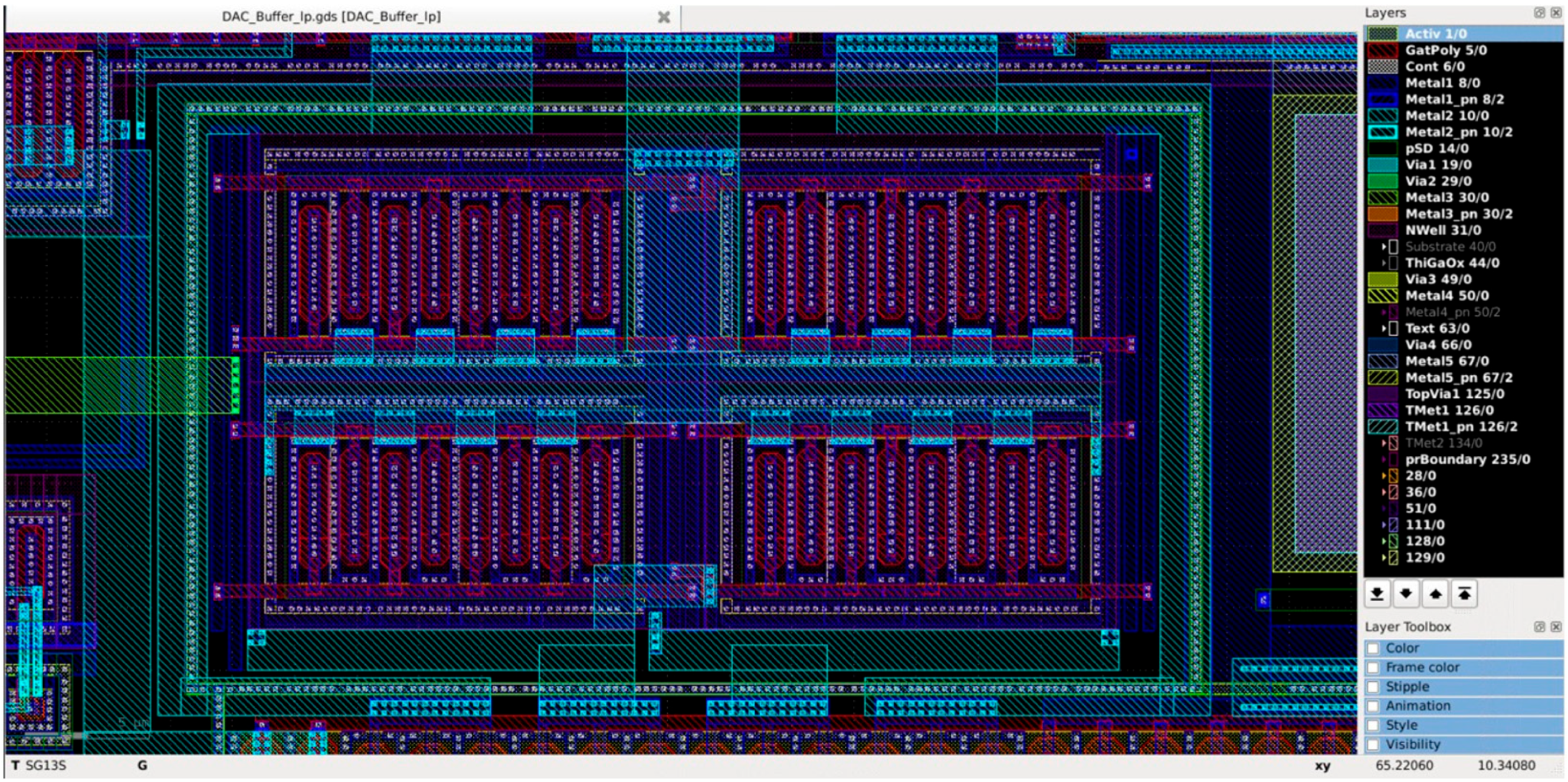
To mitigate total dose leakage as much as possible, the switch layout has been designed with an ELT (Edge-Less Transistor) shape. An example of a switch’s physical layout is shown in Figure 8. It can be noted the annular shapes of the MOS gate reduce intra-device leakage, while supply (VDD) and substrate (GND) guard rings around the transistors overcome inter-device leakage. Latch-up immunity is guaranteed by power and ground rails running in the middle between N-well and P-substrate regions; the positive feedback loop represented by vertical and lateral bipolar transistors (typical of all CMOS manufacturing processes) is cut using biased connections. The penalty in terms of area (only for EGR) is around 20% more than traditional not protected devices. There is no evident penalty for power consumption.
In the digital section, input digital latches, which freeze input bits, can be severely impacted by an SEU (Single Event Upset). Any bit flip can be avoided using robust latches (where additional capacitances are added to the most sensitive nodes) belonging to a custom rad-hard library. For this reason, TMR is not used in this work because a proven rad-hard standard cell library (including sequential cells) is employed for the DAC digital section (control logic and decoders). The clock hardness is guaranteed by short paths and a customized layout to reduce clock signal propagation. IOs are mainly analog and power supply. They do not suffer from TIDs or SELs, as input/output IO-modified pads have been used to guarantee resiliency on TIDs in the internal digital part.
The used rad-hard cells library, implemented in equivalent technologies, has been characterized in the past and validated to be resilient to a TID of 300 krad (Si), an SEU of 10 MeV × mg/cm2, and an SEL of 60 MeV × mg/cm2. To prevent SETs in the overall DAC layout, an EGR (extended guard ring, such as a triple ring of N+, P+, and N-well, etc.) is placed wherever possible.
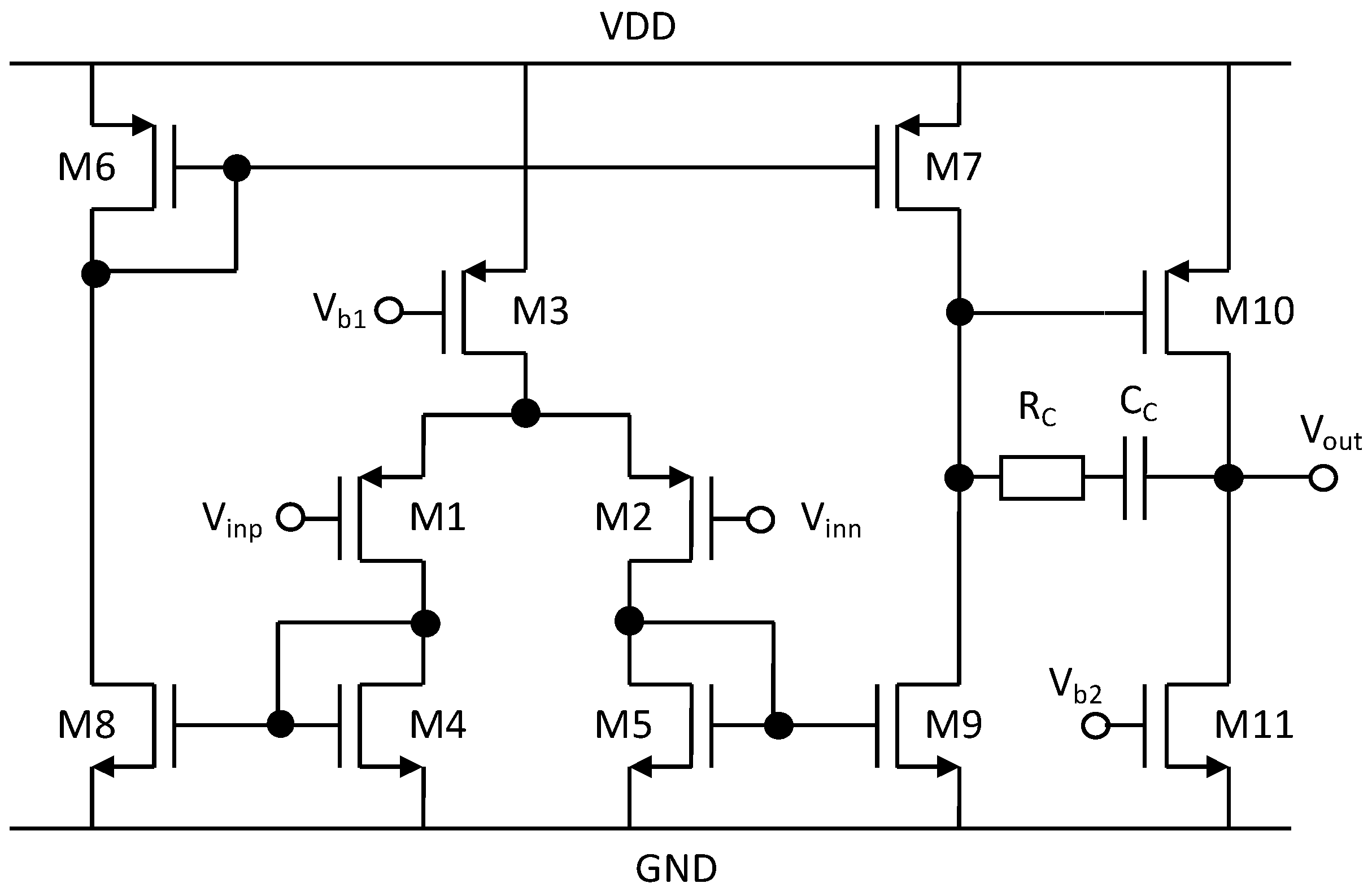
The design of the buffer required a bigger effort to avoid analog performance degradation, as well. Figure 9 shows the schematic of the main opamp. It is a two-stage opamp [28]. The first (M1–M9) is a pMOS input symmetrical stage with a mirrored topology. The signal currents generated by the input pair M1-M2 are mirrored by M4–M8 and M5–M9 and delivered to M6 and M7, respectively. The typical achievable gain is 40–50 dB. The second stage (M10–M11) is a conventional inverter with an active load, which further increases. Miller compensation (Rc − Cc) is used to achieve frequency stability. Suitable bias voltages Vb1 and Vb2 are generated by an internal circuit (not shown). Even if push–pull architectures would have guaranteed better load-driving capabilities and lower static consumption, this architecture has been chosen since it guarantees enough gain with a simple topology. Because of sensitivity to the TID, the more complex the opamp, the more probable the degradation of the opamp’s performance.
Rad-hard provisions for the opamp are mainly delegated to layout techniques. Moreover, to allow degradation under radiation, the open loop gain has been kept high. All transistors used in the buffer circuit have been sized by taking into consideration the radiation tests reported in the literature (not minimum W and L) and by applying an ELT shape. The matching of the input pair mainly determines the opamp offset, which reflects a shift in the DAC transfer curve. The radiation-induced threshold voltage shift does not influence the transistor threshold voltage mismatch, as assessed in [29]. We applied a variant of the common centroid topology of an ELT MOS to achieve the physical matching of the input stage. For example, the MOS of the input pair (M1, M2) has a width equal to 160 um each. They have been split into 16 ELTs, each of them placed in a “common centroid” way (Figure 10). In the active load and bias circuits, we have applied the same technique.
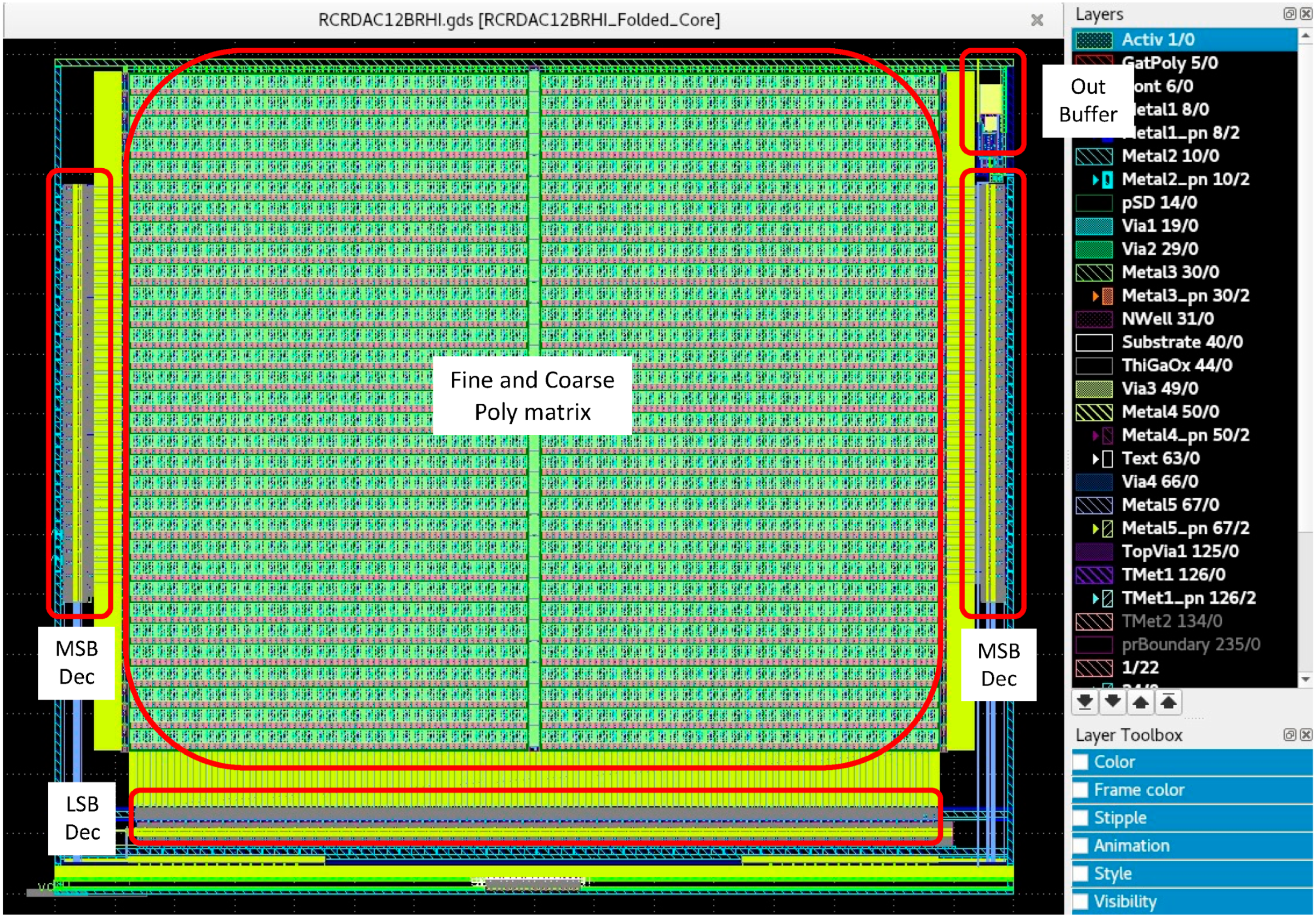
The DAC layout is shown in Figure 11 with different blocks identified by labels. Its area is 1.6 mm × 1.4 mm (2.24 mm2). The percentage of area occupation for the various blocks is 75% for the matrix (resistor plus switches); 8% for the logic; <1% for the output buffer; and the rest are at 16% for the signal and supply routing.

4. Test Results

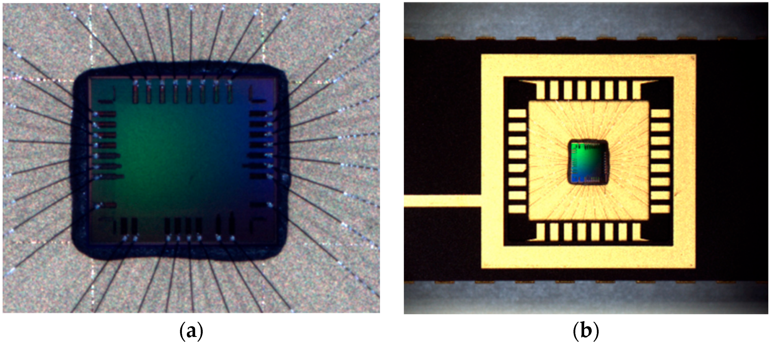
The resistor string DAC has been integrated into a standard 3.3 V 130 nm CMOS process (IHP SG13S). Figure 12 shows the micro-photo (a) and the assembled component (b) in a 32-pin CERDIP (Ceramic Dual-in-Line Package). The overall chip area is 2.5 mm × 2.25 mm (5.62 mm2), including the padframe.

4.1. In-Lab Measurements

The prototypes have been first characterized both in terms of static and dynamic performance. The DAC output voltage range has been set to 1.5 Vpp. The DNL and INL (presented in Figure 13) have been measured by utilizing the so-called “major carrier method” [30], which can be applied for monotonic converters like ours and allows us to save an amount of stored data and time testing time.
The measured DNL is less than ±0.15 LSB, while the INL is less than ±0.2 LSB. These excellent results have been obtained thanks to the accurate layout of the resistor matrix adopting the folded approach and an extensive procedure of try–extract–simulate–repeat. These results make the converter very fitting to be used in DC or quasi-static applications and on-board satellites.
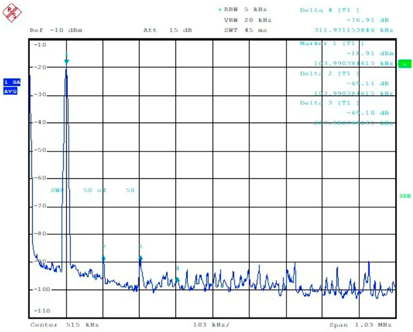
The dynamic performance has been measured by applying a sinewave and using a clock of 1 MS/s and a clock of 3 MS/s. Figure 14 shows the spectrum of the buffered output when a 33 kHz 1.5 Vpp sinewave with a clock of 1 MS/s is applied, while Figure 15 reports the spectrum when a 100 kHz 1.5 Vpp sinewave with a clock of 3 MS/s is used. The ENOB is higher than 10.8 bits for 1 MS/s and 9.5 bits at 3 MS/s. The ENOB represents the number of bits when both noise and total harmonics distortion are considered. At 3 MS/s, the ENOB degrades approximately to one bit. The DAC remains operative at 2 Vpp, but the SFDR is degraded by 5 dB.
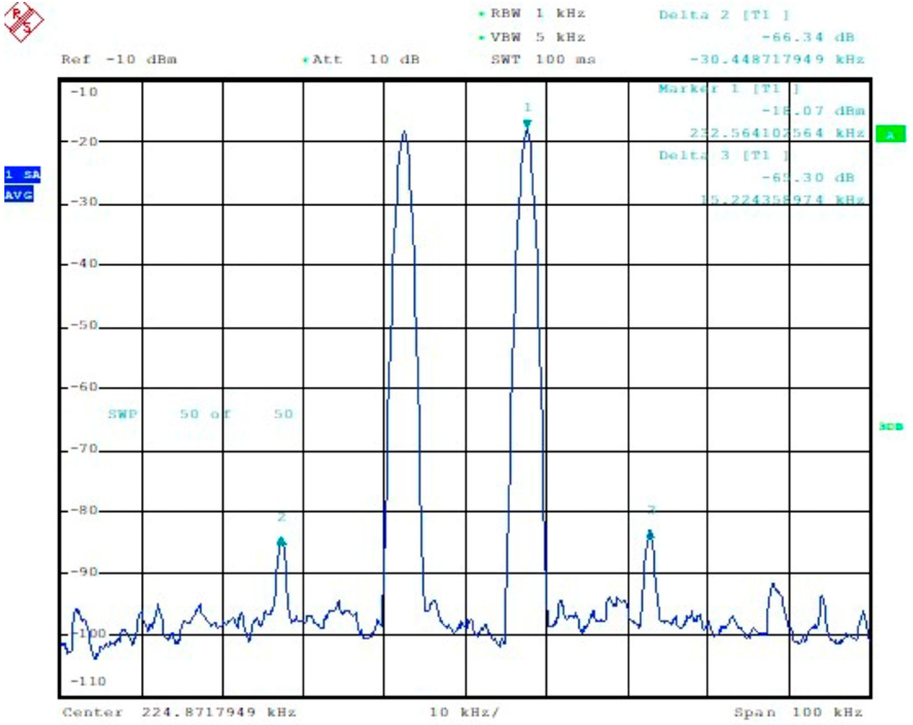
Intermodulation (IMD) performance (IP3) has been measured, as well. A pair of tones equal to 217.4 kHz + 232.6 kHz are applied with a clock of 1 MS/s at 65 dBc (Figure 16). IMD decreases at 56 dBc when the tones are equal to 652.174 kHz + 697.674 kHz at a clock of 3 MS/s.
Core power consumption from the supply is below 10 mW with a 3.3 V supply (<200 uW in power down) plus string current consumption. The main part of the consumption is due to the output buffer, driving a capacitive load of 10 pF. The string current consumption is approximately 0.39 mA for a 1.5 V output voltage range.
The proposed DAC architecture is modular and can be easily downscaled. Indeed, the authors also designed a 10-bit version of the DAC intended as a macro for less resolution-demanding applications [5]. Measured DNL and INL performances were quite similar to those of 12 bits (DNL < ±0.1 LSB and INL < ±0.1 LSB), while distortion performance is slightly better at a higher clock frequency (3 MS/s), achieving an ENOB of 9.7 LSBs.
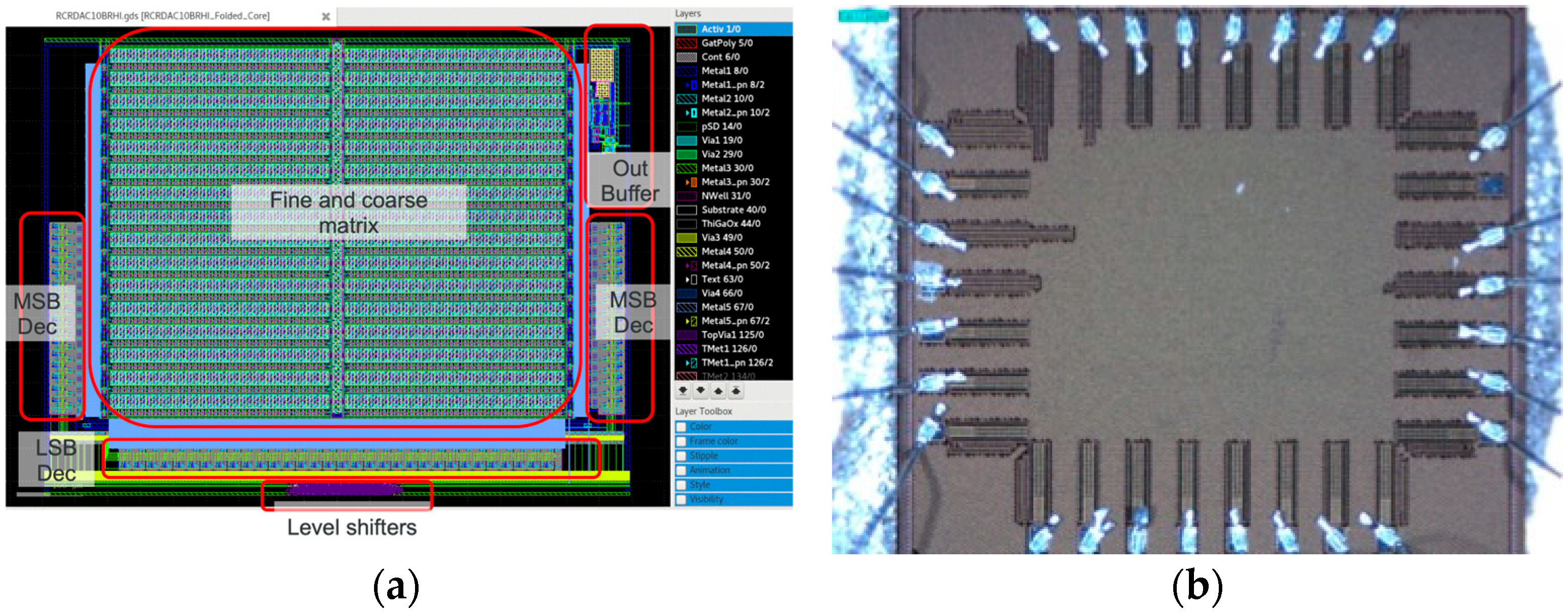
The layout (a) and chip photo (b) of the 10-bit DAC are shown in Figure 17. The macro DAC size is now 890 μm × 700 μm (0.62 mm2), approximately one-quarter that of the 12-bit DAC, as expected.

4.2. Measurements under Radiation

The rad-hard 12-bit DAC has been tested under Cobalt 60 at the University of Palermo facility using the RedCat Devices proprietary Leonida Platform. Using a 0.63 rad/s dose rate, the DAC reached 500 krad (Si) with no significant degradation in terms of performance.
By considering the harsh conditions of the environment (rich in radiation), a new testing strategy shall be defined. The traditional measurements performed using a test board where the Device Under Test (DUT) is mounted and a lab set up with equipment suitable to generate waveforms and collect the outputs are not viable. Only the DUT shall be exposed, while the measurement equipment and auxiliary active circuitry cannot be placed under or near the irradiation beams. Remote control of all measurement operations is necessary.
The proposed solution is based on splitting the test board in the following:
  • A motherboard (MB), which hosts the signal generation, data acquisition system, and auxiliary circuitry;
  • A daughterboard (DB) with the DUT only.
The DB is connected to the MB hosting the control electronics with the DUT by means of flat cables for digital signals and coax cables for critical analog signals.
The MB can be designed in several ways. Depending on the application, it can be a custom board or an off-the-shelf board. The former can contain whatever electronic is needed, with only mechanical constraints, but it has cost penalties, and a specific control software should be developed. The latter, despite being less flexible, is cheaper and can leverage the available development software. We adopted the second approach using an Arduino Due® (Arduino S.r.l., Monza, Italy) [31]. To add more flexibility, we developed a small shield board (a board that can be assembled on top of an Arduino board) with some additional functions (Figure 18). Arduino Due hosts on-board digital signal generators (for the generation of bits), accurate ADCs for the reading of the proposed 12-bit DAC output voltage and current consumption, and two DACs to generate the DUT voltage references. The shield includes two LN (Low Noise) buffers for DUT references and current references and LDO for supply and current sense.
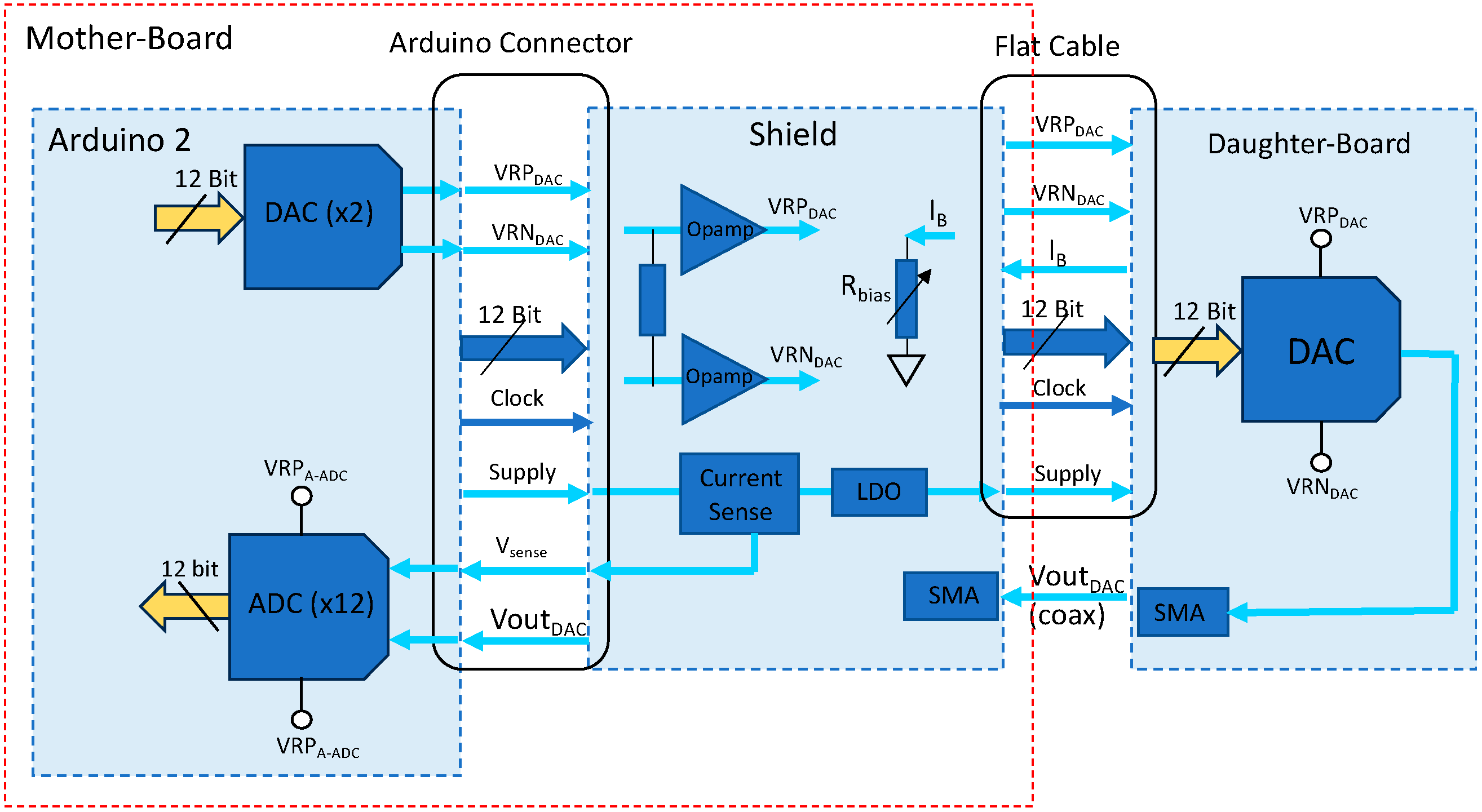
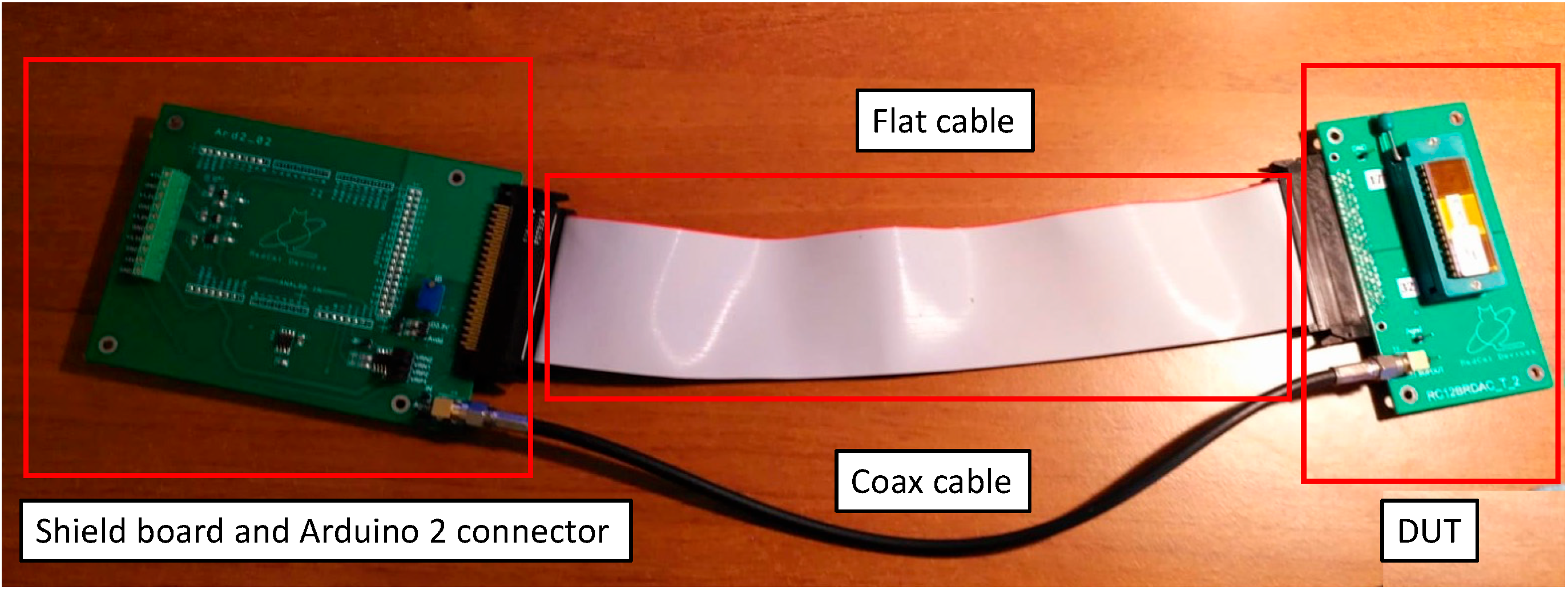
A complete block diagram of the three boards employed for testing under radiation is shown in Figure 19, while a photo of the complete system is presented in Figure 20.
As can be seen, in this case, a flat cable manages digital signals while the coaxial cable connects the DAC analog output to the Arduino ADC. Since working frequencies are not so high, a signal integrity analysis is not mandatory, with the exception of some special cases, such as a data converter clock.
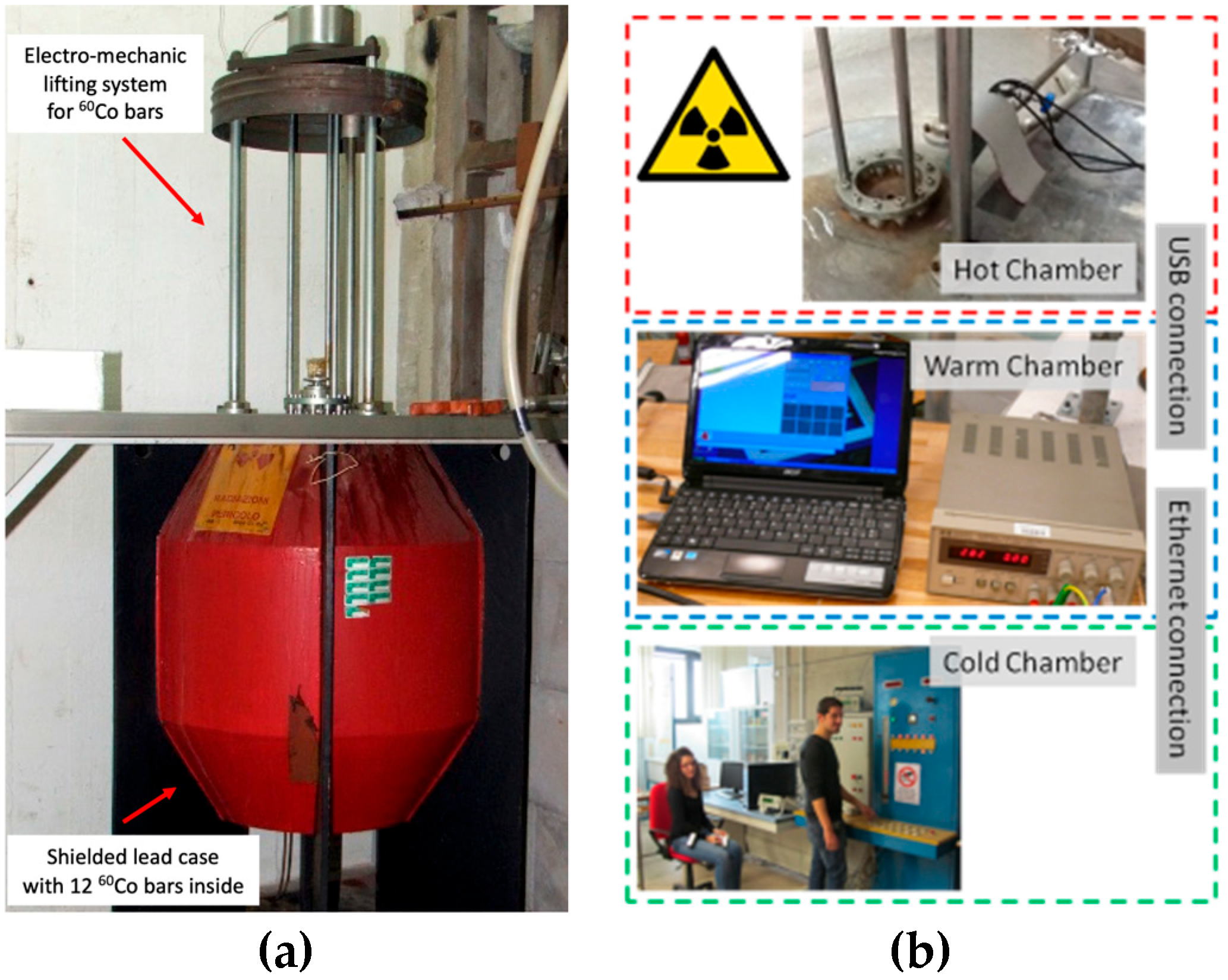
The facility environment for the test is organized into three rooms: a hot room, a warm room, and a control room. The hot room contains the IGS-3 gamma irradiator (see Figure 21a) equipped with a total of 4.31 TBq of 60Co gamma-ray source and the two test boards.
The control PC and minor instruments are then placed outside the irradiation cell in a shielded room (called a “warm room”) where radiation cannot cause damage. Finally, all equipment within the warm room is remotely managed from the cold room (or control room), which is fully shielded and allows safe access for people (Figure 21b).
The presence of different working rooms leads to difficulties in managing irradiation testing of electronic devices working in active operations. The three rooms are connected with USB and ethernet connections, and it is also possible to remotely control the PCs in the cold chamber by means of a remote terminal application.
In the hot chamber, the Arduino motherboard is shielded by means of lead bricks, while the daughterboard with the DUT is exposed. Figure 22a shows the shielding box (built with lead bricks) still open. The MB is placed inside (the other board is not related to the DAC test), and Figure 22b shows the placement of the MB (protected in the closed shielding box) and DB (exposed). A dosimeter placed near the DUT (not shown in the photo) verifies the exposition rate.
The approach used for DNL and INL measurements in this specific case is the one shown in Figure 23. The test bits are applied to the DUT; the DAC output voltage is converted to digital by the ADC hosted in the Arduino Due board, and its output bits are recorded remotely by the developed software (Leonida Platform Ver. 20230301). The obtained data can be kept as they are or converted again in analog by means of the following equation:
(VRPADC − VRNADC/4095) × ADCoutcode + Voffset,ADC
where VRPADC and VRNADC are ADC references, ADCoutcode is the measured digital code, and Voffset,ADC is the offset of the ADC. The Arduino ADC references (as measured before the test) are fixed and and are equal to VRPADC =3.3 V and VRNADC = 30 mV, and its LSB = 0.798 mV.
For the TID measures, we have applied three digital input codes in sequence to the DAC (corresponding to 0, half-range, and full range) and recorded the code feed by means of the ADC on Arduino Due. We have also recorded the static power consumption due mainly to the analog part, as read by the current sense circuit.
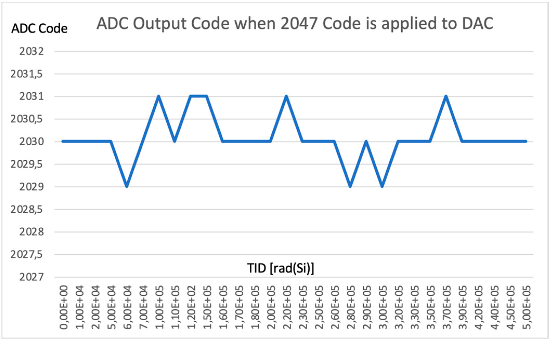
Figure 24 shows the Arduino ADC output code when the 2027 code is applied to the DAC. The absolute median value (2030) is not coincident (or near) to 2047 since, as said, the Arduino ADC has an offset with respect to the DAC range. So, while the DAC output half-range voltage is perfectly 1.65 V (VDD/2), the ADC input half-range voltage is approximately 1.665 V, 15 mv (or 18 LSB). By adding 18 to 2030, we obtain 2048, which is almost coincident with the DAC half-range. We verified that up to 500 krad (Si) read codes remain within ±1 LSB, which is mainly due to the uncertainty in the measure (Figure 24).
A slightly worse behavior has been measured for 0 and 4095 codes, with an uncertainty of ±2 LSB, which always stays the same up to 500 krad (Si).
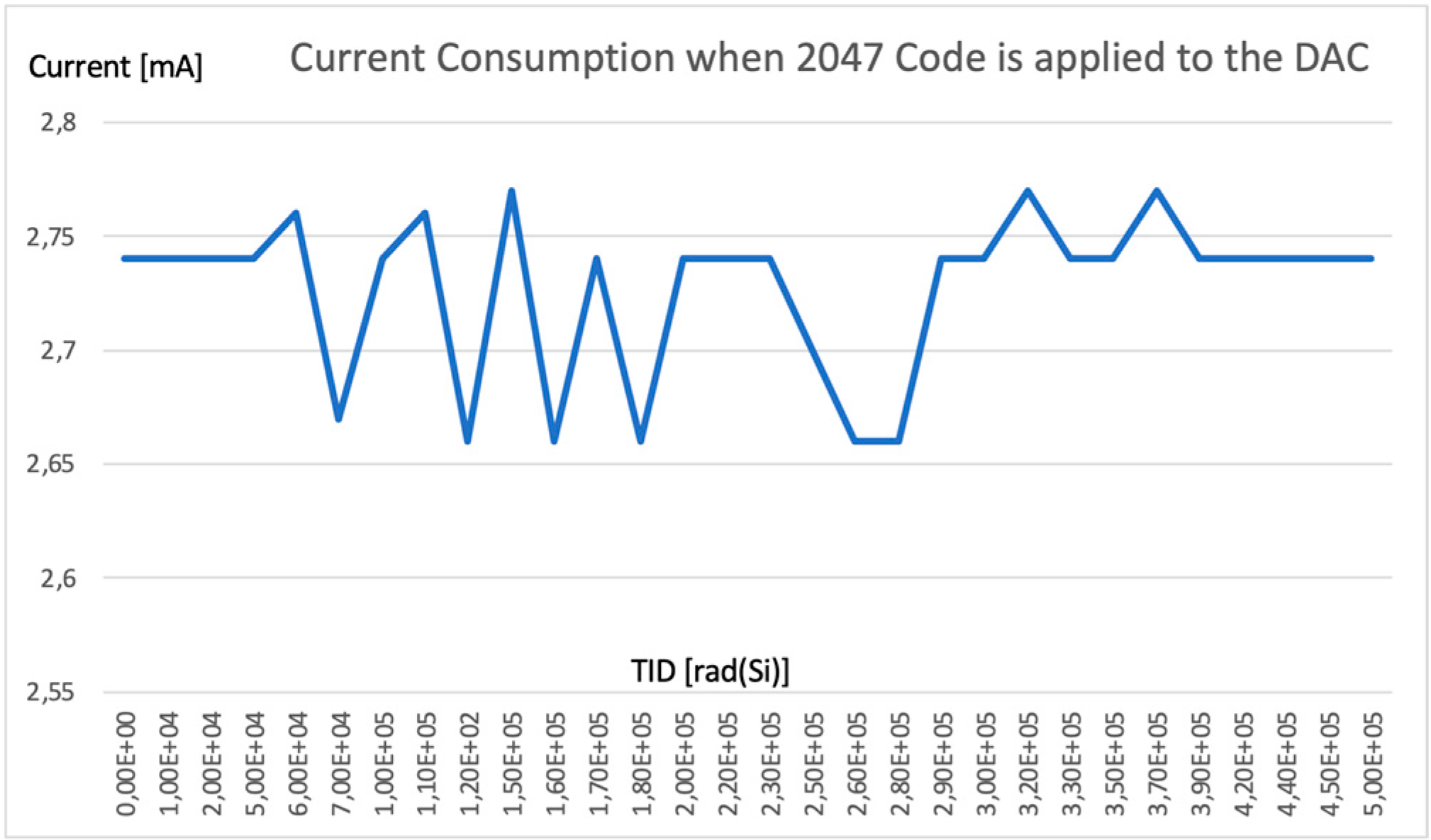
Current consumption is measured by means of a current sense circuit placed on the shield board. It generates a voltage that is proportional to the supply current flowing across it. Its value is then converted by the Arduino ADC and recorded by the Leonida Platform. The measured analog current consumption in mA is shown in Figure 25 when the half-range code is applied to the DAC input. As can be seen, apart from an uncertainty in the measure (due, for example, to low voltage drop on current sense and ADC finite resolution), it is almost constant around 2.7 mA up to 500 krad (Si), as shown in Figure 25.
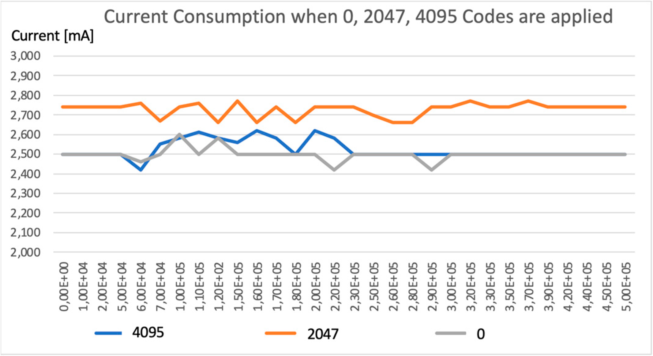
Moreover, in Figure 26, there is a comparison of DAC current consumption as a function of radiation dose for the three codes, 0, 2047, and 4095. As shown, the consumption is higher for the 2047 code, depending on the operation of the DAC output buffer.
On the other side, digital current consumption is very low and impulsive, with an average value <300 uA, which does not significantly change with the TID.
Table 2 presents a comparison of the proposed work with the referenced rad-hard DACs present in the literature. As can be seen, our DAC is competitive while using a standard process (bulk CMOS). This is a strong point since the process is cheaper than BiCMOS and allows the integration of the DAC macro in a more complex chip where a significant digital part is present. Its resiliency performance is superior to that of the others; DLN/INL is in line, while the occupied area is even lower.
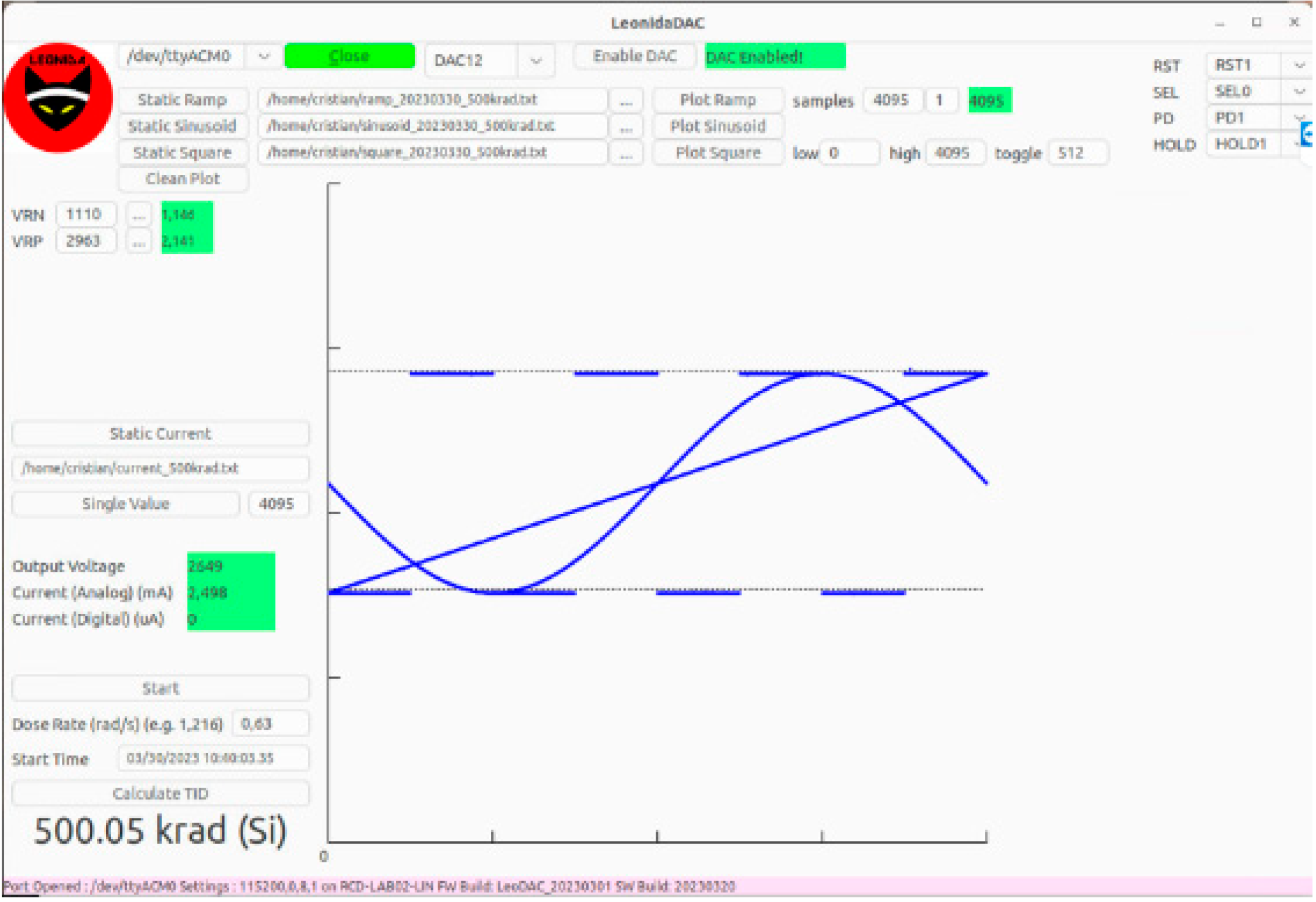
Finally, it is worth noting that the Leonida Platform (the control software), in addition to single codes, can also generate ramps of codes, square waves, or sinewaves, as shown in Figure 27. It shows the GUI (Graphics User Interface) of the Leonida Platform that allows us to control several items of the experiment remotely. For example, the upper section allows us to set the filename where acquired data (output DAC voltage) will be stored, the kind of forcing signal to the DAC (ramp, sinusoid, or square), and how many samples are used for it. The graphs at the center of the picture are the representation of the forcing signal.
The section on the right side of the graph at the top allows us to fix positive and negative voltage references for the DAC. Further down, it is possible to force a single DC value to the DAC and to immediately read the measured output voltage.

5. Conclusions

In this paper, we have presented a rad-hard 12-bit DAC integrated in a 0.13 um CMOS IHP technology. Starting from the most popular topologies and considering requirements on resiliency, we have chosen the resistive architecture. It has been evaluated as the most convenient both in terms of simplicity and radiation hardness. The measured INL is less than ±0.2 LSB and DNL is less ±0.15 LSB. The obtained ENOB is 9.5 bits at a data rate of 3 MS/s. The DAC has been tested under Cobalt 60 at the University of Palermo facility using the RedCat Devices proprietary Leonida Platform and new testing strategies. Measured performance shows no significant degradation up to 500 krad (Si) of ionizing radiation, confirming the effectiveness of the methodology based on the so-called RHBD.
The proposed DAC architecture is modular and can be easily downscaled by acting on decoder size and a fine coarse matrix while maintaining the same floorplan. The 12-bit DAC, together with its downscaled version and the ADC already developed [32], constitute the basis for the creation of a library of rad-hard data converters as IP macro-blocks in conventional bulk CMOS processes.

Author Contributions

Conceptualization: C.C. and U.G.; Validation: C.C. and U.G.; Writing: C.C. and U.G.; Review and Editing: C.C. and U.G. All authors have read and agreed to the published version of the manuscript.

Funding

This research was funded by the EU Horizon 2020 Moral “Export-free Rad-hard Microcontroller for Space Applications” project (grant agreement No. 870365).

Institutional Review Board Statement

Not applicable.

Informed Consent Statement

Not applicable.

Data Availability Statement

Data are contained within the article.

Acknowledgments

The authors would like to thank Marcello Donati and Armando Colamonico (ABC Progetti) for the in-lab testing campaign and Aldo Parlato and Elio Tomarchio for the test at the Palermo University irradiation facility.

Conflicts of Interest

Cristiano Calligaro and Umberto Gatti were employed by the company RedCat Devices. Authors declare that the research was conducted in the absence of any commercial or financial relationships that could be construed as a potential conflict of interest.

References

  1. Bourdarie, S.; Xapsos, M. The near-earth space radiation environment. IEEE Trans. Nucl. Sci. 2008, 55, 1810–1832. [Google Scholar] [CrossRef]
  2. Calligaro, C.; Gatti, U. Rad-Hard Semiconductor Memories; River Publisher: Nordjylland, Denmark, 2018; ISBN 9788770220200. [Google Scholar]
  3. Calligaro, C.; Arbat, A.; Roizin, Y.; Nahmad, D. A 15 Mrad (Si) 512Kbit Rad-Hard SRAM in a standard 0.18um CMOS technology. In Proceedings of the 3th European Conference on Radiation and its Effects on Components and Systems (RADECS) 2012, Biarritz, France, 24–28 September 2012. [Google Scholar]
  4. Mueller, S.; Weigel, R.; Koelpin, A. A Survey on Analog-to-Digital Converter Performance with Respect to Ionizing Radiation. In Proceedings of the 2017 17th European Conference on Radiation and Its Effects on Components and Systems (RADECS), Geneva, Switzerland, 2–6 October 2017; pp. 1–4. [Google Scholar]
  5. Calligaro, C.; Gatti, U. A CMOS 10-Bit 3MS/s Rad-Hard DAC Based on Resistor String Poly-Matrix. In Proceedings of the 2021 IEEE 32nd International Conference on Microelectronics (MIEL), Nis, Serbia, 12–14 September 2021. [Google Scholar]
  6. Tsiligiannis, G.; Makris, K.; Lambaounas, T.; Fragopoulos, D.; Anagnostopoulos, P.; Papadas, C.; Schoellkopf, J.P.; Glass, B. A Very High Resolution DAC at 1kHz for Space Applications. In Proceedings of the 2010 NASA/ESA Conference on Adaptive Hardware and Systems, Anaheim, CA, USA, 15–18 June 2010. [Google Scholar]
  7. Karaolis, M.; Stafylidis, A.; Dokianaki, O.; Papathanasiou, K.; Makris, K.; Fragopoulos, D.; Papadas, C.; Glass, B. High Resolution Radiation Hardened DAC in CMOS-SOI Featuringa Return-to-Zero Matrix. In Proceedings of the AMICSA 2016, Gothenburg, Sweden, 12–16 June 2016. [Google Scholar]
  8. Cressler, G.; Mantooth, H. (Eds.) Extreme Environment Electronics; CRC Press: Boca Raton, FL, USA, 2013. [Google Scholar]
  9. Axness, C.L.; Riewe, L.; Reber, R.A.; Liang, A.Y.; Ang, S.S.; Brown, W.D. Radiation Characteristics of SIPOS and Polysilicon Resistors. IEEE Trans. Nucl. Sci. 1991, 38, 1365–1369. [Google Scholar] [CrossRef]
  10. Irom, F.; Agarwal, S.G. Compendium of Single-Event Latchup and Total Ionizing Dose Test Results of Commercial Digital to Analog Converters. In Proceedings of the. 2015 IEEE Radiation Effects Data Workshop (REDW), Boston, MA, USA, 13–17 July 2015. [Google Scholar]
  11. Stone, S.E.; Lombardi, R.E.; Seehra, S.S.; Likar, J.J.; Begovic, J.; Herschitz, R. Single Event Effects Characterization of Maxwell 7846B DAC. In Proceedings of the 2012 IEEE Radiation Effects Data Workshop, Miami, FL, USA, 16–20 July 2012. [Google Scholar]
  12. Karakozov, A.B.; Nekraso, P.V.; Bobrovsky, D.V.; Sorokoumov, G.S.; Telets, V.A. Single Event Effects and Total Dose Testing of Digital to Analog Converters. In Proceedings of the 17th European Conference on Radiation and Its Effects on Components and Systems (RADECS), Geneva, Switzerland, 2–6 October 2017. [Google Scholar]
  13. Daniel, A.C.; Vartanian, S.; Allen, G.R. Radiation Effects Characterization of Commercial Multi-Channel Digital to Analog Converters for Spaceflight Applications. In Proceedings of the 2019 IEEE Radiation Effects Data Workshop, San Antonio, TX, USA, 8–12 July 2019. [Google Scholar]
  14. Kruckmeyer, K.; Prater, J.S.; Brown, B.; Trinh, T. Analysis of Low Dose Rate Effects on Parasitic Bipolar Structures in CMOS Processes for Mixed-Signal Integrated Circuits. IEEE Trans. Nucl. Sci. 2011, 58, 1023–1031. [Google Scholar] [CrossRef]
  15. Fan, H.; Li, D.; Zhang, K.; Cen, Y.; Feng, Q.; Qiao, F.; Heidari, H. A 4-Channel 12-Bit High-Voltage Radiation-Hardened Digital-to-Analog Converter for Low Orbit Satellite Applications. IEEE Trans. Circuits Syst.–I 2018, 65, 3698–3706. [Google Scholar] [CrossRef]
  16. Chen, Z.; Dai, F.F. A 3mW 8-Bit Radiation-hardened-by-design DAC for Ultra-wide Temperature Range from −180 °C to 120 °C. In Proceedings of the 2011 IEEE International Symposium of Circuits and Systems (ISCAS), Rio de Janeiro, Brazil, 15–18 May 2011; pp. 997–1000. [Google Scholar]
  17. Kim, D.; Kwon, I.; Kim, C.-H. A 10-bit Radiation-Hardened R-2R Digital-to-Analog Converter for Nuclear Power Plant Applications. In Proceedings of the Transactions of the Korean Nuclear Society Spring Meeting, Jeju, Republic of Korea, 23–24 May 2019. [Google Scholar]
  18. Yao, Y.; Dai, F.; Jaeger, R.C.; Cressler, J.D. A 12-Bit Cryogenic and Radiation-Tolerant Digital-to-Analog Converter for Aerospace Extreme Environment Applications. IEEE Trans. Ind. Electron. 2008, 55, 2810–2818. [Google Scholar]
  19. Kunnath, A.T.; Sahoo, B. A Digitally Assisted Radiation Hardened Current Steering DAC. In Proceedings of the 2016 29th International Conference on VLSI Design and 2016 15th International Conference on Embedded Systems (VLSID), Kolkata, India, 4–8 January 2016; pp. 559–560. [Google Scholar]
  20. Dugoujon, L.; Papadas, C.; Sinnis, B. A 0.13 µm CMOS Rad-hard proven technology with associated mixed mode circuit design approaches for space applications. In Proceedings of the AMICSA, Xanthi, Greece, 2–3 October 2006. [Google Scholar]
  21. Haddad, N.F.; Kelly, A.T.; Lawrence, R.K.; Li, B.; Rodgers, J.C.; Ross, J.F.; Warren, K.M.; Weller, R.A.; Mendenhall, M.H.; Reed, R.A. Incremental enhancement to SEU hardened 90 nm CMOS memory cell. In Proceedings of the RADECS 2010, Längenfeld, Austria, 20–24 September 2010. [Google Scholar]
  22. Clark, L.T.; Mohr, K.C.; Holbert, K.E.; Yao, X.; Knudsen, J.; Shah, H. Optimizing Radiation Hard by Design SRAM Cells. IEEE Trans. Nucl. Sci. 2007, 54, 2028–2036. [Google Scholar] [CrossRef]
  23. Anelli, G.; Campbell, M.; Delmastro, M.; Faccio, F.; Floria, S.; Giraldo, A.; Heijne, E.; Jarron, P.; Kloukinas, K.; Marchioro, A.; et al. Radiation Tolerant VLSI Circuits in Standard Deep Submicron CMOS Technologies for the LHC Experiments: Practical Design Aspects. IEEE Trans. Nucl. Sci. 1999, 46, 1690–1696. [Google Scholar] [CrossRef]
  24. Jacob Baker, R. (Ed.) CMOS Circuit Design, Layout, and Simulation; IEEE Press: Piscataway, NJ, USA, 1998. [Google Scholar]
  25. Pelgrom, M. A 50 MHz 10-bit CMOS digital-to-analog converter with 75 Ω buffer. J. Solid-State Circuits 1990, 25, 1347–1352. [Google Scholar] [CrossRef]
  26. Gatti, U.; Calligaro, C.; Pikhay, E.; Roizin, Y. Radiation-hardening methodologies for Flash ADC. Analog Integr. Circuits Signal Process. 2016, 87, 141–154. [Google Scholar] [CrossRef]
  27. Maloberti, F. Analog Design for CMOS VLSI Systems; Springer: Berlin/Heidelberg, Germany, 2001. [Google Scholar]
  28. Vergine, T.; De Matteis, M.; Michelis, S.; Traversi, G.; De Canio, F.; Baschirotto, A. A 65 nm Rad-Hard Bandgap Voltage Reference for LHC Environment. IEEE Trans. Nucl. Sci. 2016, 63, 1762–1767. [Google Scholar] [CrossRef]
  29. Verbeeck, J.; Leroux, P.; Steyaert, M. Radiation effects upon the mismatch of identically laid out transistor pairs. In Proceedings of the 2011 IEEE ICMTS International Conference on Microelectronic Test Structures, Amsterdam, The Netherlands, 4–7 April 2011; pp. 194–197. [Google Scholar]
  30. Burns, M.; Roberts, G.W. An Introduction to Mixed-Signal IC Test and Measure; Oxford University Press: Oxford, UK, 2001. [Google Scholar]
  31. Available online: https://docs.arduino.cc/hardware/due/ (accessed on 18 April 2023).
  32. Kuentzer, F.; Tittlebach-Helmrich, K.; Cueto, J.; Garcia Donday, F.; Schmidt, M.; Schommer, B.; Ferdinand, C.; Soding-Freiherr von Blomberg, A.; Calligaro, C.; Gatti, U. Rad-hard Microcontroller with Open Access ISA for Space Applications. In Proceedings of the 9th International Workshop on Analogue and Mixed-Signal Integrated Circuits for Space Applications, Madrid, Spain, 31 May–3 June 2022. [Google Scholar]
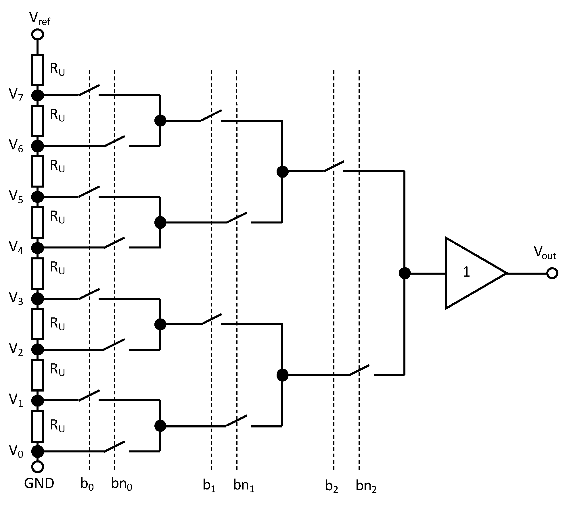
Figure 1. Resistor string DAC (Kelvin divider for 3 bits).
Chips 03 00006 g001
Figure 2. Matrix resistor string (folded resistor string for 4 bits).
Chips 03 00006 g002
Figure 3. Schematic of the X-Y resistor matrix DAC [5,25].
Chips 03 00006 g003
Figure 4. Complete block diagram of the full DAC.
Chips 03 00006 g004
Figure 5. Monte Carlo simulations for process and mismatch variation (1000 runs): RCx = RFy = 61 ohm [5].
Chips 03 00006 g005
Figure 6. Straight layout (a) and folded layout (b) of a resistor string.
Chips 03 00006 g006
Figure 7. Floorplan of the 12-bit DAC.
Chips 03 00006 g007
Figure 8. Layout of the switch used as a coarse and fine selector in the DAC matrix [5].
Chips 03 00006 g008
Figure 9. Schematic of the opamp used as the DAC output buffer [5] (all nMOS bodies are tied to the ground, the pMOS M1 and M2 bodies are tied to the source).
Chips 03 00006 g009
Figure 10. Layout of the opamp input differential stage with a common centroid ELT.
Chips 03 00006 g010
Figure 11. Layout of the 12-bit DAC macro.
Chips 03 00006 g011
Figure 12. Chip photo (a) and packaged 12-bit DAC (b).
Chips 03 00006 g012
Figure 13. Measured DNL (a) and INL (b) of the DAC.
Chips 03 00006 g013
Figure 14. Measured spectrum of the buffered output when a 33 kHz 1.5 Vpp sinewave with a clock of 1 MS/s is applied (ENOB = 10.8 Bit).
Chips 03 00006 g014
Figure 15. Measured spectrum of the buffered output when a 100 kHz 1.5 Vpp sinewave with a clock of 3 MS/s is applied (ENOB = 9.5 Bit).
Chips 03 00006 g015
Figure 16. Measured IMD (IP3) when the buffered output of two tones with a clock of 1 MS/s is applied (IMD = 65 dBc).
Chips 03 00006 g016
Figure 17. Layout (a) and chip photo (b) of the 10-bit DAC macro [5].
Chips 03 00006 g017
Figure 18. Detail of the Arduino 2 board plus a custom shield.
Chips 03 00006 g018
Figure 19. Block diagram of the boards used for tests under irradiation.
Chips 03 00006 g019
Figure 20. Photo of the complete system (MB + DB) for the DAC test of the TID.
Chips 03 00006 g020
Figure 21. Photos of the IGS-3 gamma irradiator (a) and the “logical” split of environments and Hw connections (b).
Chips 03 00006 g021
Figure 22. (a) Shielding box (with lead bricks) still open with the MB; (b) placement of the MB (protected) and DB (exposed).
Chips 03 00006 g022
Figure 23. DNL-INL test block diagram.
Chips 03 00006 g023
Figure 24. ADC output code as a function of radiation dose.
Chips 03 00006 g024
Figure 25. DAC analog current consumption as a function of radiation dose for the half-range DAC.
Chips 03 00006 g025
Figure 26. DAC analog current consumption as a function of radiation dose for three codes: 0, 2047, and 4095.
Chips 03 00006 g026
Figure 27. Snapshot of the Leonida Platform.
Chips 03 00006 g027
Table 1. Sensitivity of DAC architectures to radiations [5].
ResistiveCapacitiveCurr. Steer.
TIDKKΛ
SETϑΛϑ
SELKKK
RHBD-ALLowHighHigh
RHBD-CLMediumMediumHigh
RHBD-LLMediumMediumMedium
Table 2. Performance comparison with some rad-hard DACs taken from the literature.
This Work[15][18][16][17] **[19]
Resolution12 bits12 bits8 bits12 bits12 bits10 bits
Technology130 nm CMOS0.5 um
BiCMOS
0.5 um SiGe BiCMOS0.5 um SiGe BiCMOS65 nm CMOS130 nm CMOS
ArchitectureX-Y
R Matrix
R-2RR-2RSegmented Current SteeringCurrent SteeringCurrent Steering
Data Rate3 MS/s100 kS/s10 MS/s80 MS/sNA15 MS/s
DNL±0.15 LSB±0.23 LSB±0.2 LSBNANANA
INL±0.2 LSB±0.67 LSB±0.3 LSBNANANA
SFDR69 dBcNA55 dBc54 dBcNANA
ENOB9.5 bitsNANANANA8.73 bits
TID500 krad (Si)20 krad (Si)NA300 krad (Si)100 Mrad (Si)NA
Supply+3.3 V±15 V+3.3 V+3.3 V+1.2 V+1.2 V
Area2.24 mm220 mm2,*0.25 mm26.3 mm2,***NANA
* Four channels of the DAC; ** only the simulation was provided; *** includes pads.
Disclaimer/Publisher’s Note: The statements, opinions and data contained in all publications are solely those of the individual author(s) and contributor(s) and not of MDPI and/or the editor(s). MDPI and/or the editor(s) disclaim responsibility for any injury to people or property resulting from any ideas, methods, instructions or products referred to in the content.