
A Review on Fundamentals of Noise-Shaping SAR ADCs and Design Considerations

 , , and
Abstract
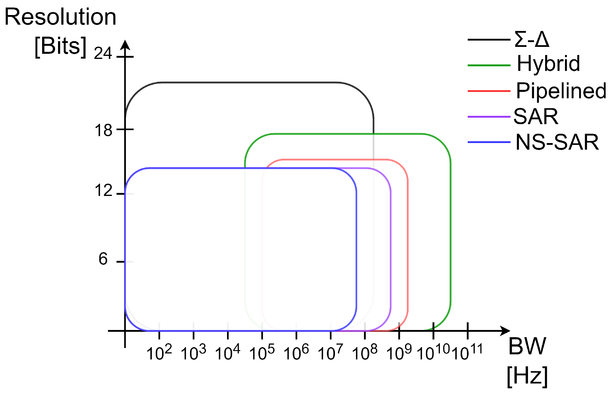
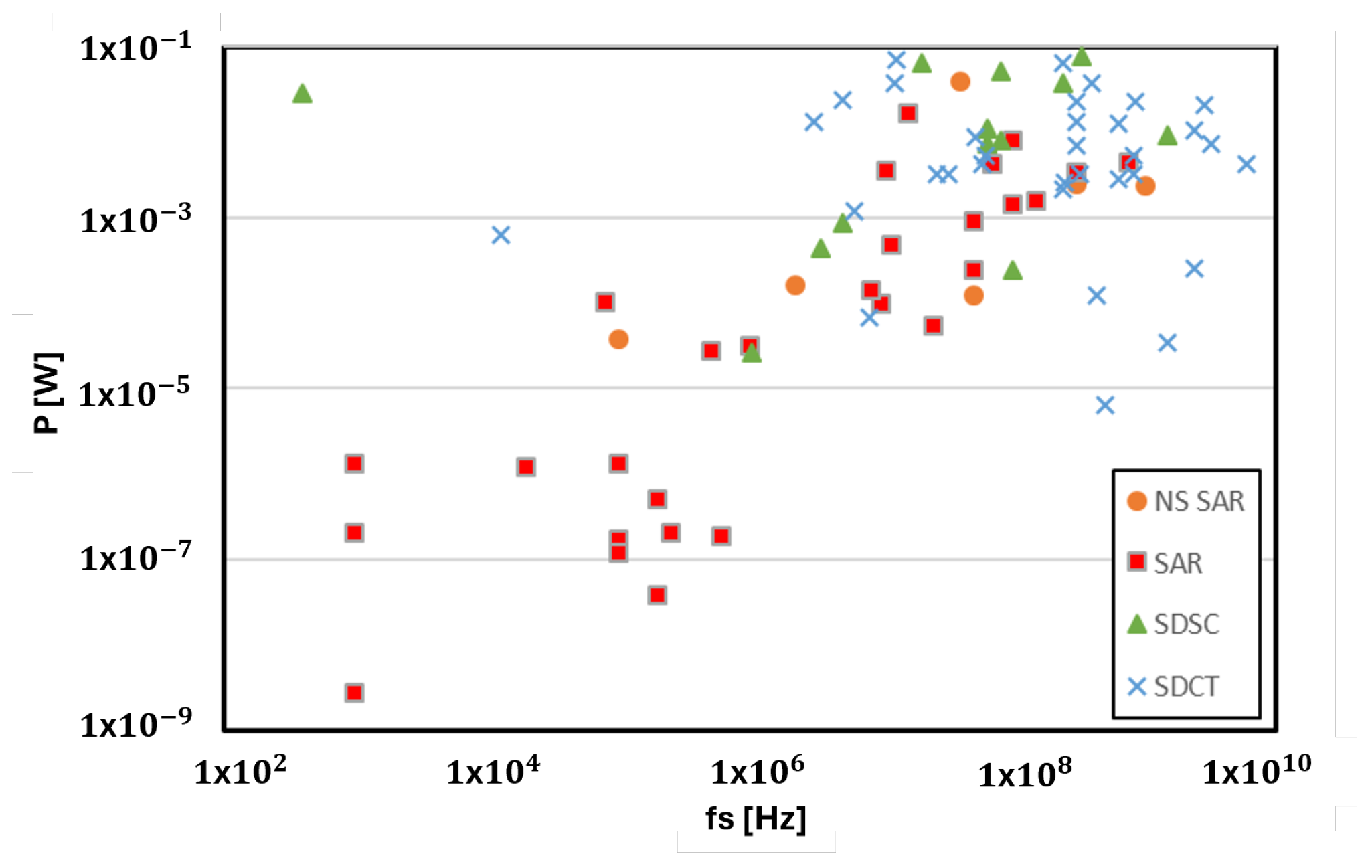
1. Introduction
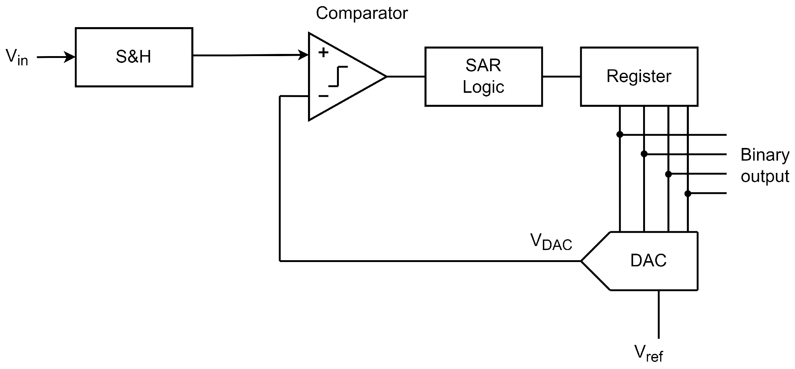
2. From SAR ADC to NS SAR: Fundamentals
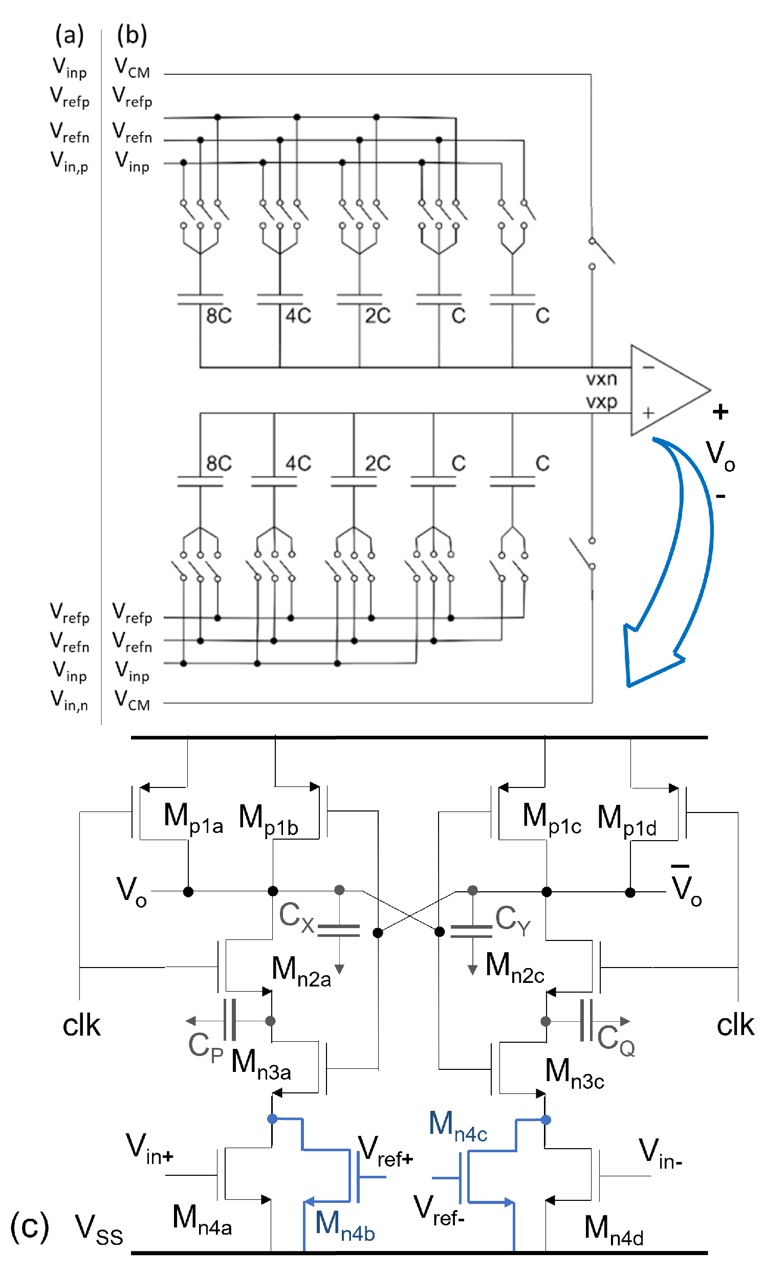
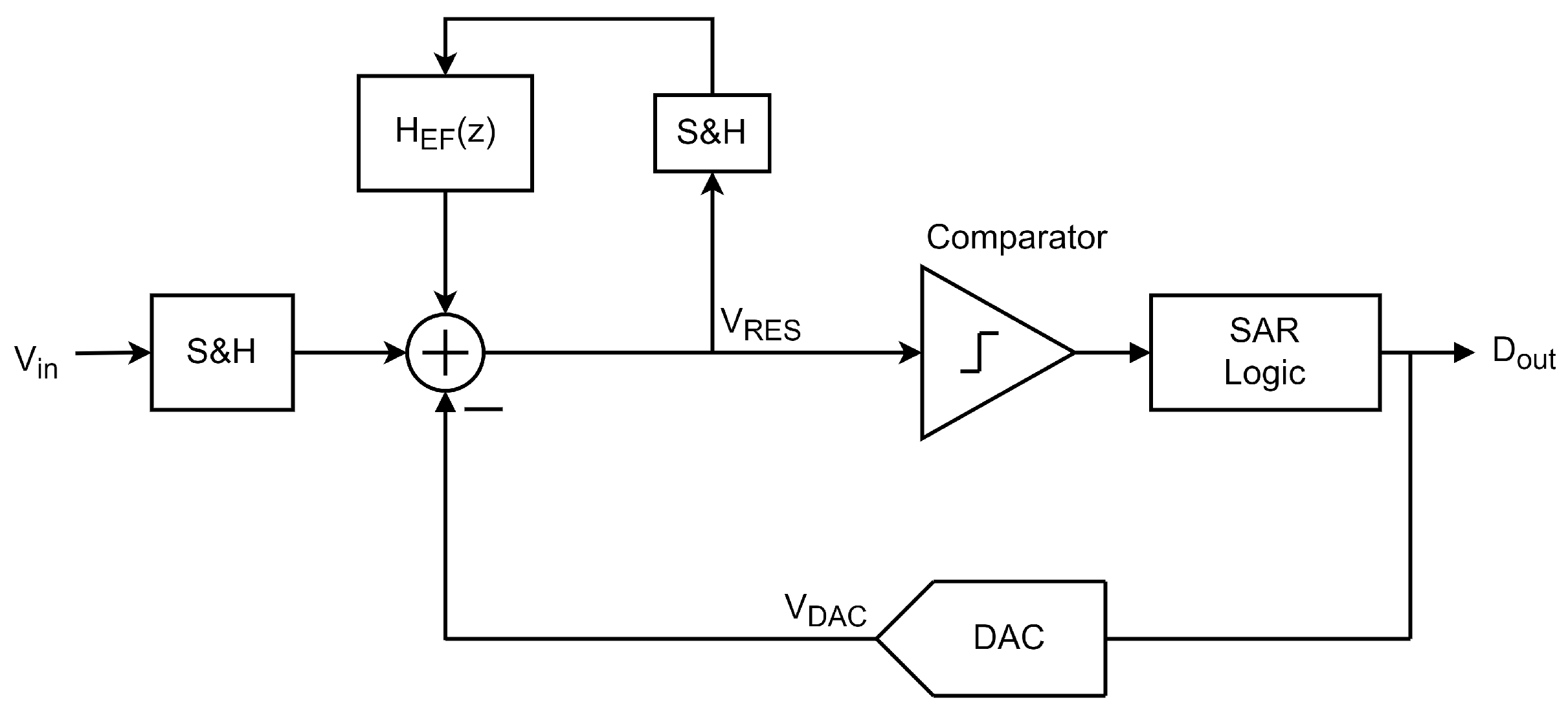
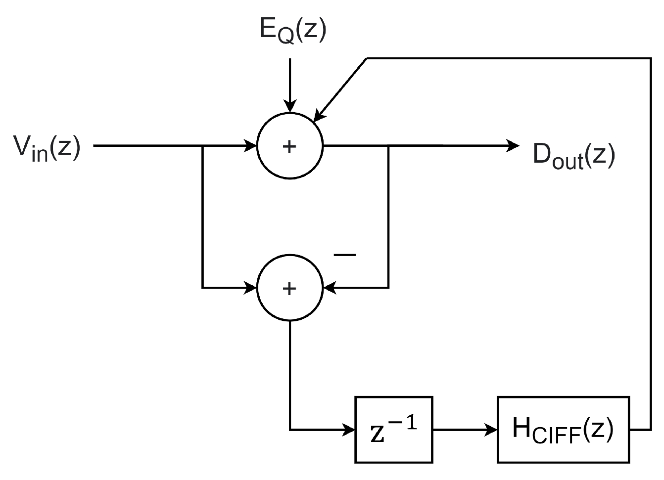
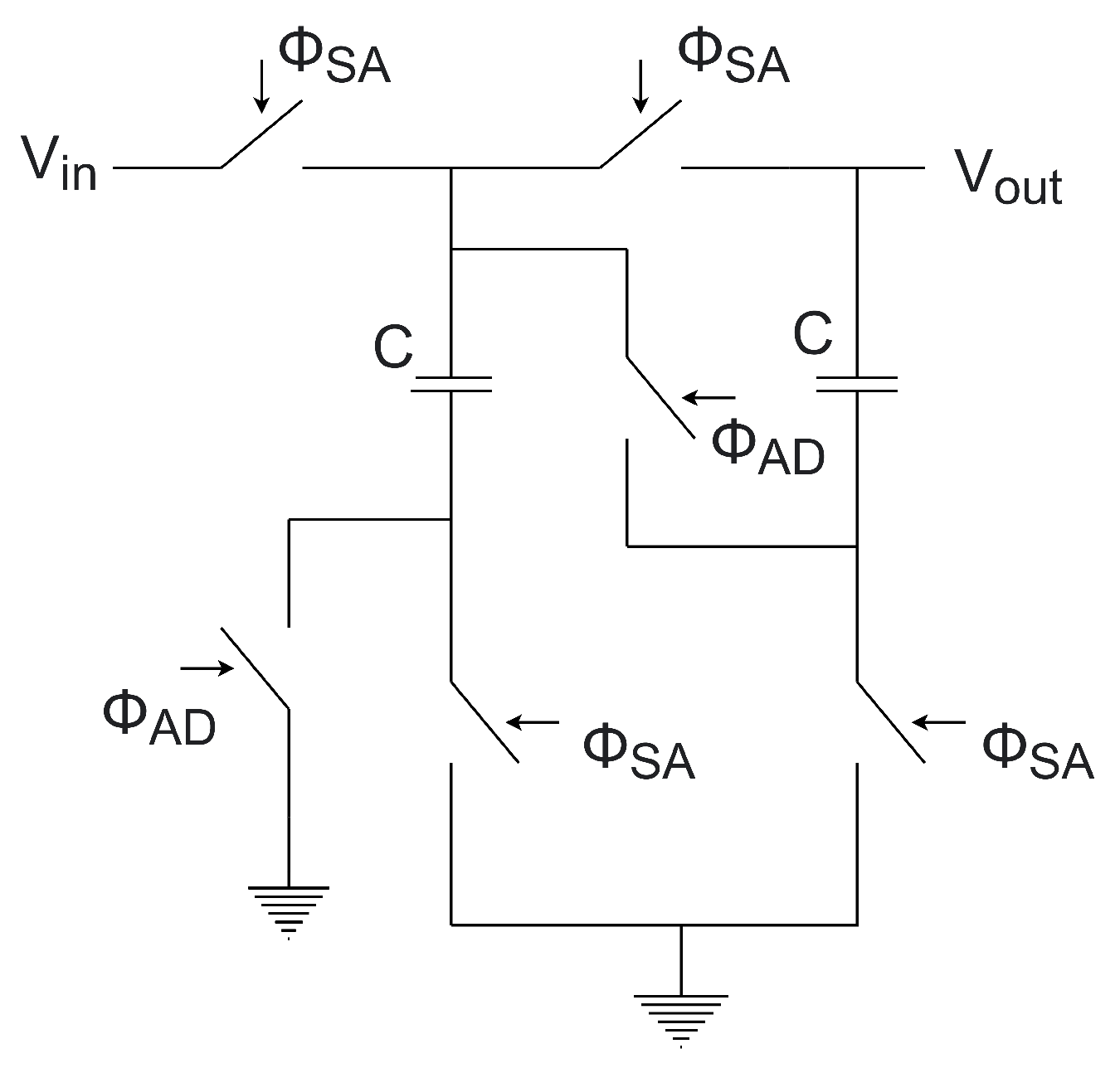
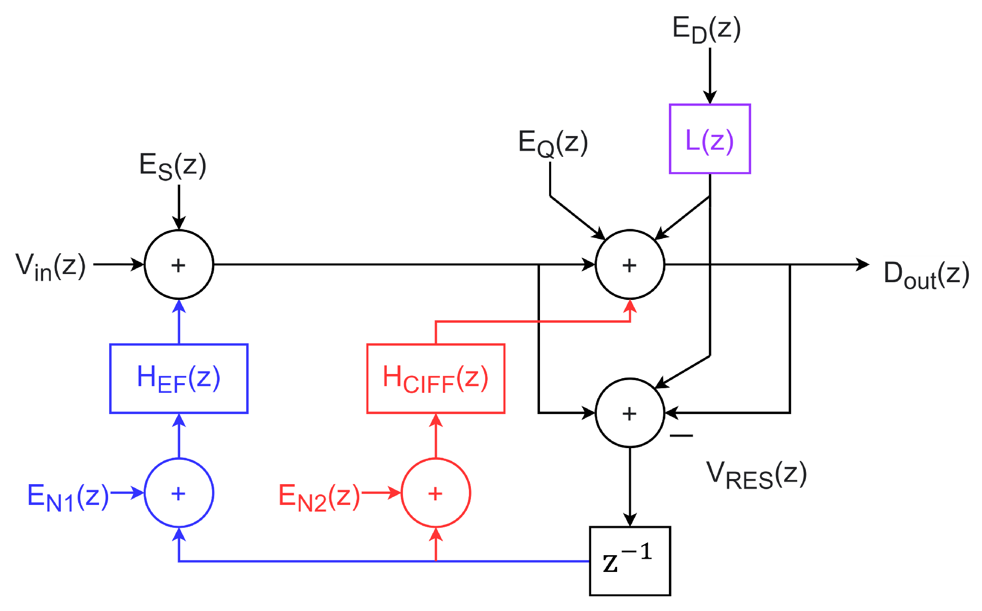
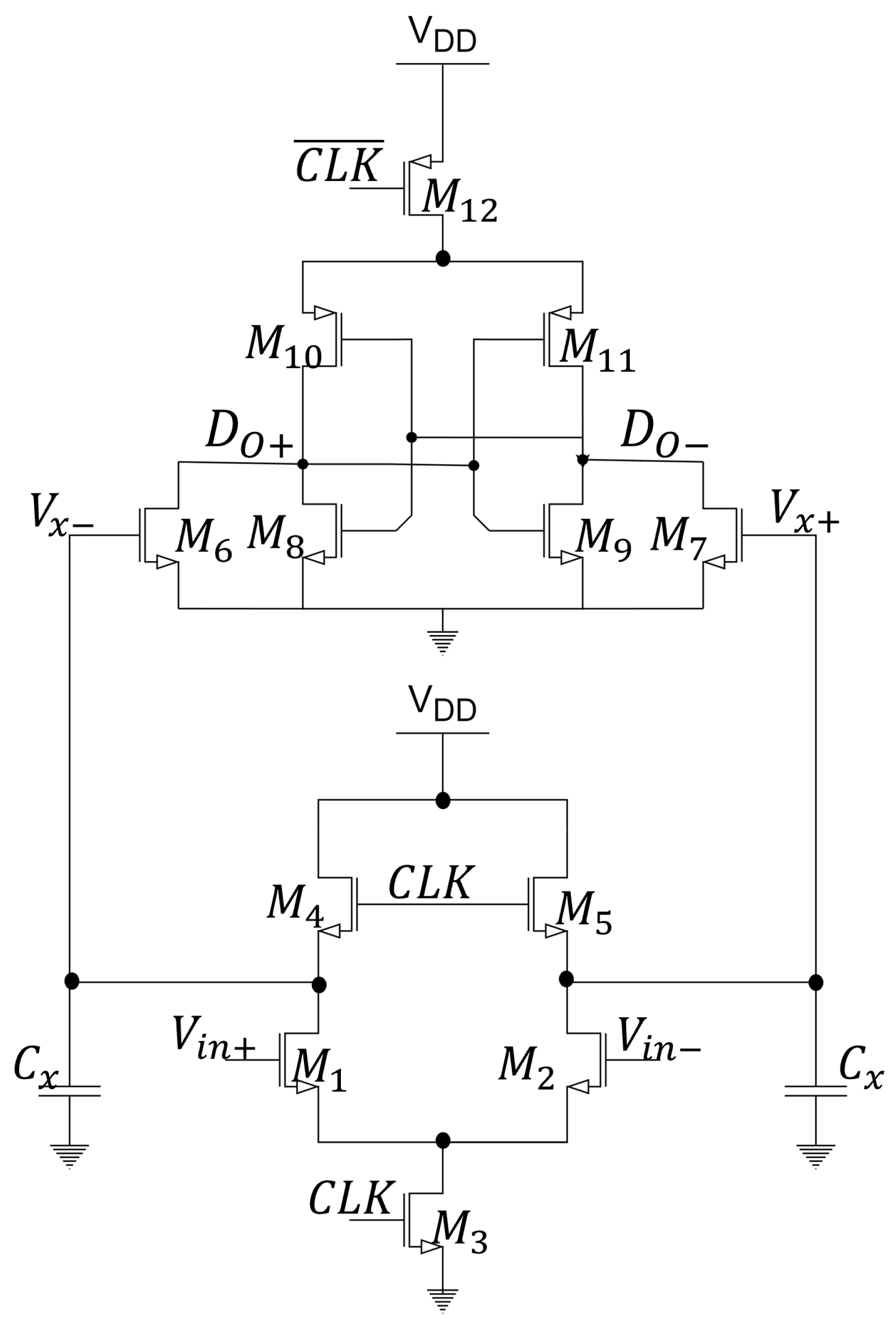
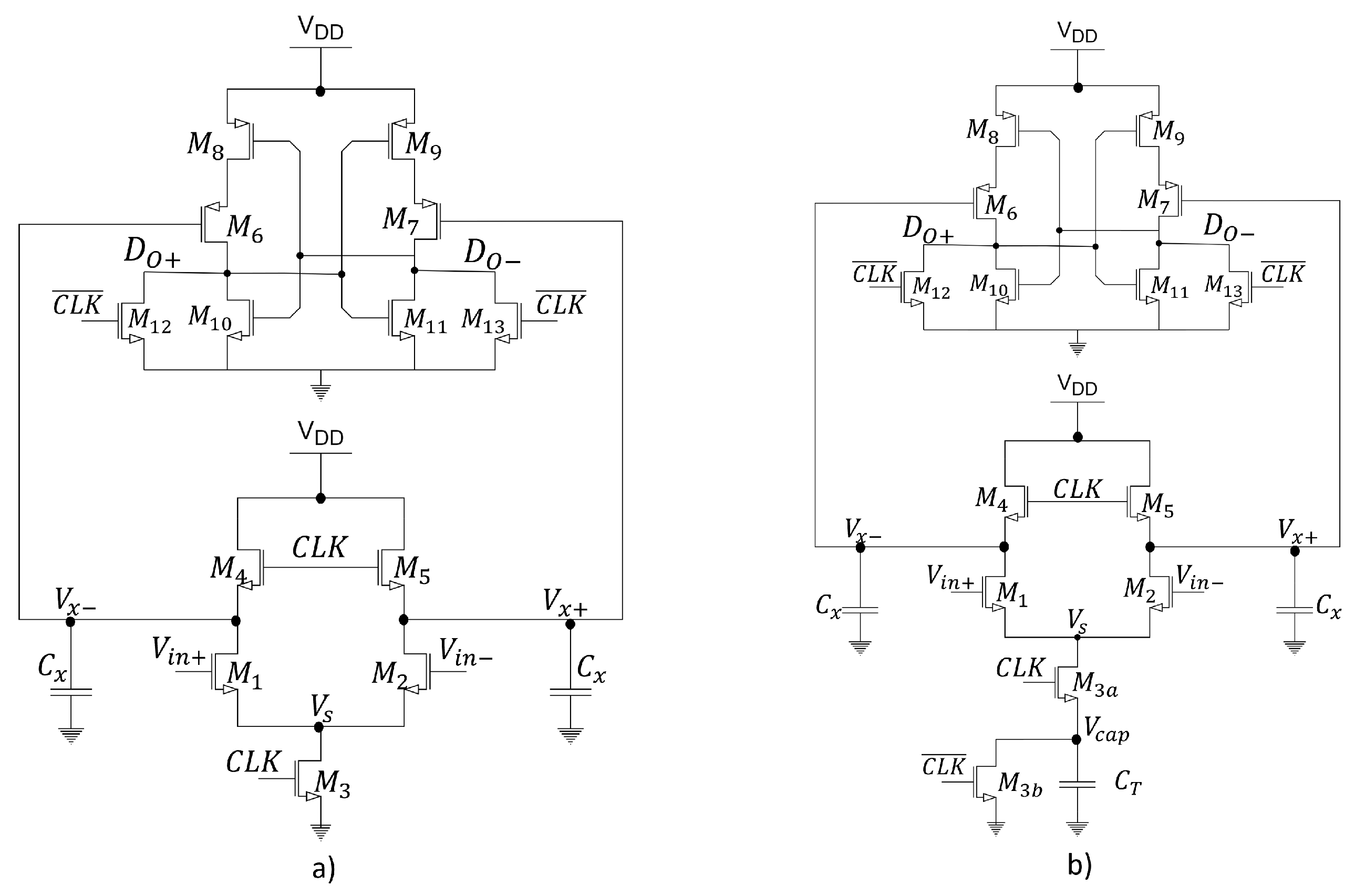
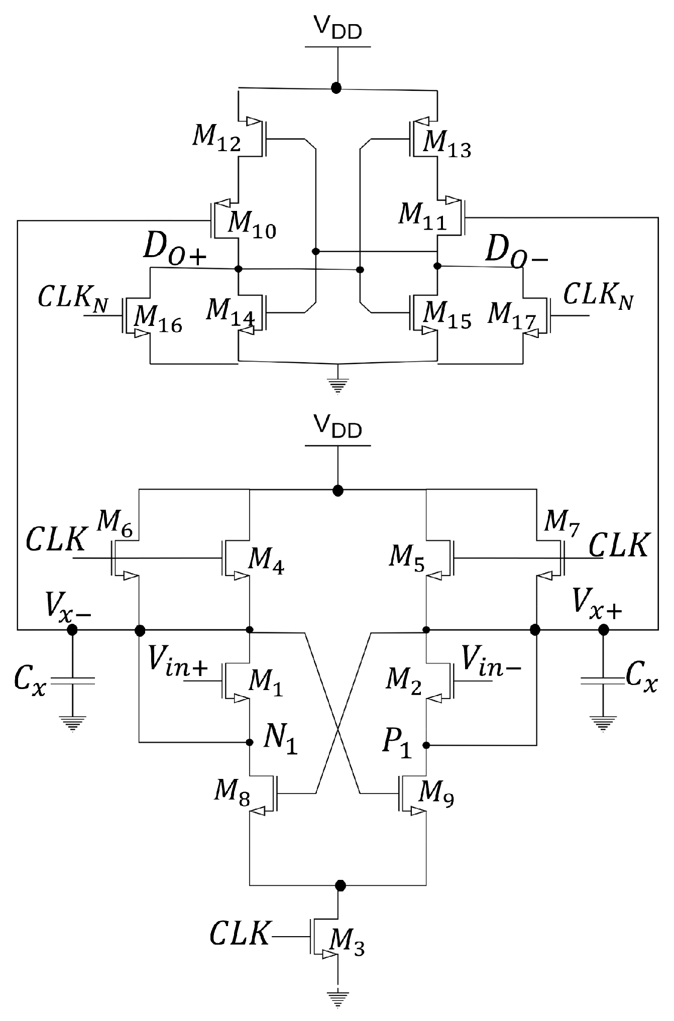
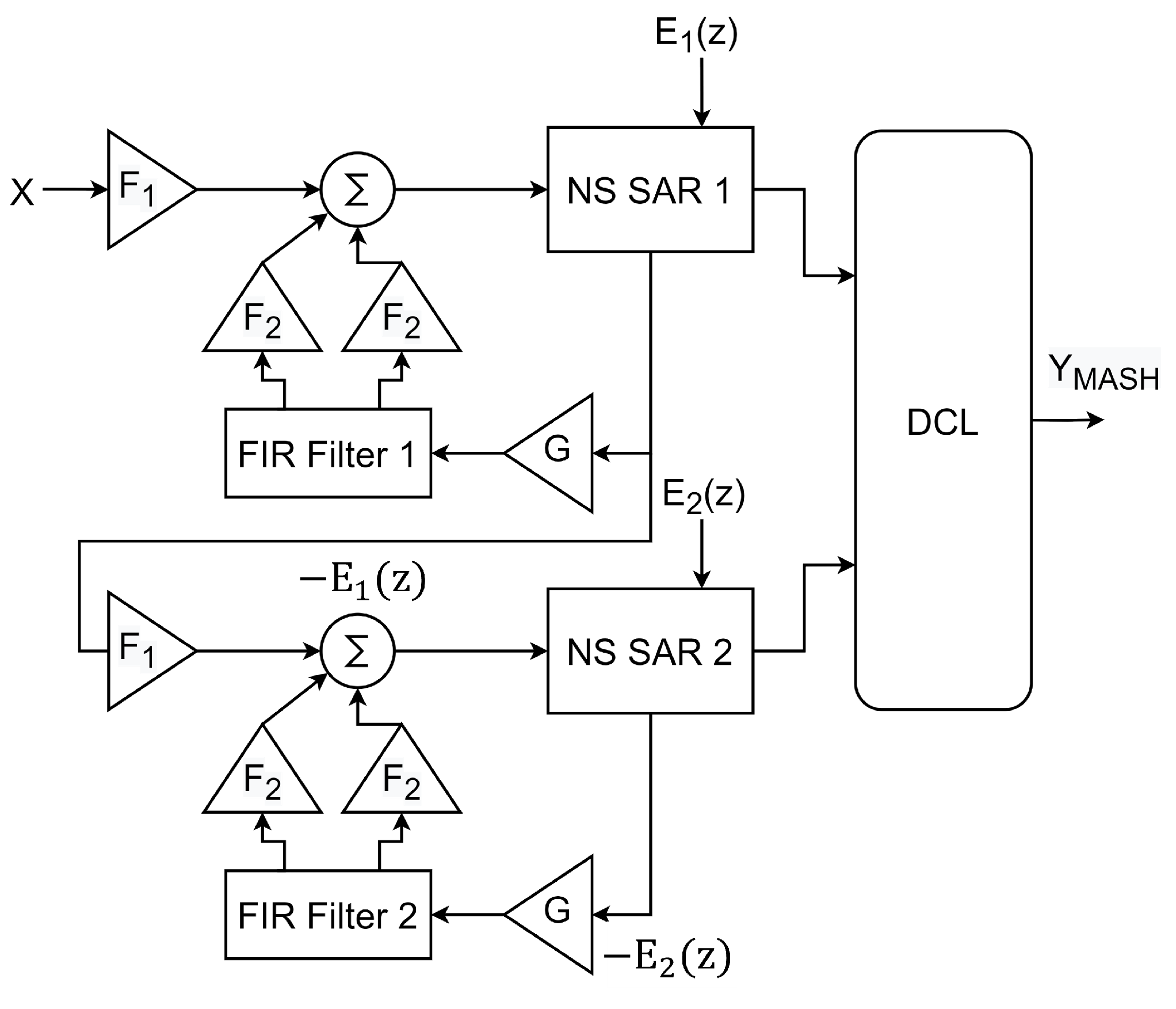
2.1. Noise-Shaping SAR ADC Implementations: Error-Feedback and Cascade Integrator Feed-Forward

| Specification | Chen 2015 [13] | Li 2018 [17] | Yi 2022 [14] |
|---|---|---|---|
| Filter | EF | EF | EF |
| Process | 65 nm | 40 nm | 65 nm |
| Order | 1 | 2 | 1 |
| Supply | 0.8 V | 1.1 V | 1.2 V |
| Bits | 8 | 9 | 9 |
| BW | 6.25 MHz | 625 kHz | 625 kHz |
| OSR | 4 | 8 | 16 |
| SNDR | 58.03 dB | 79 dB | 81 dB |
| Power | 120.7 µW | 84 µW | 183.6 µW |
| FoMs | 165.1 dB | 178 dB | 176.3 dB |
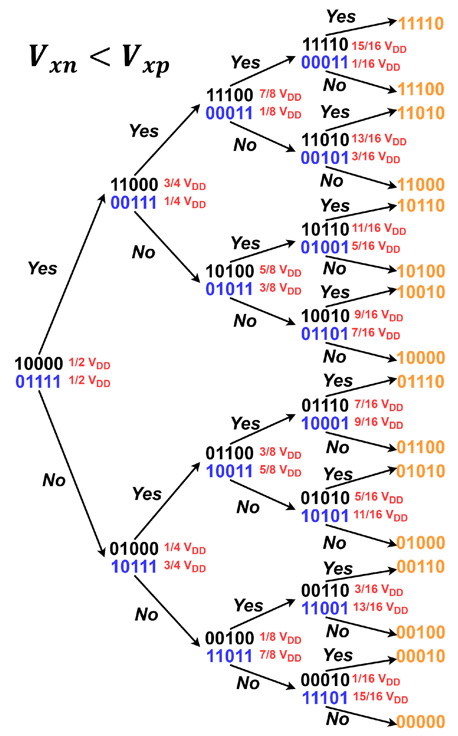
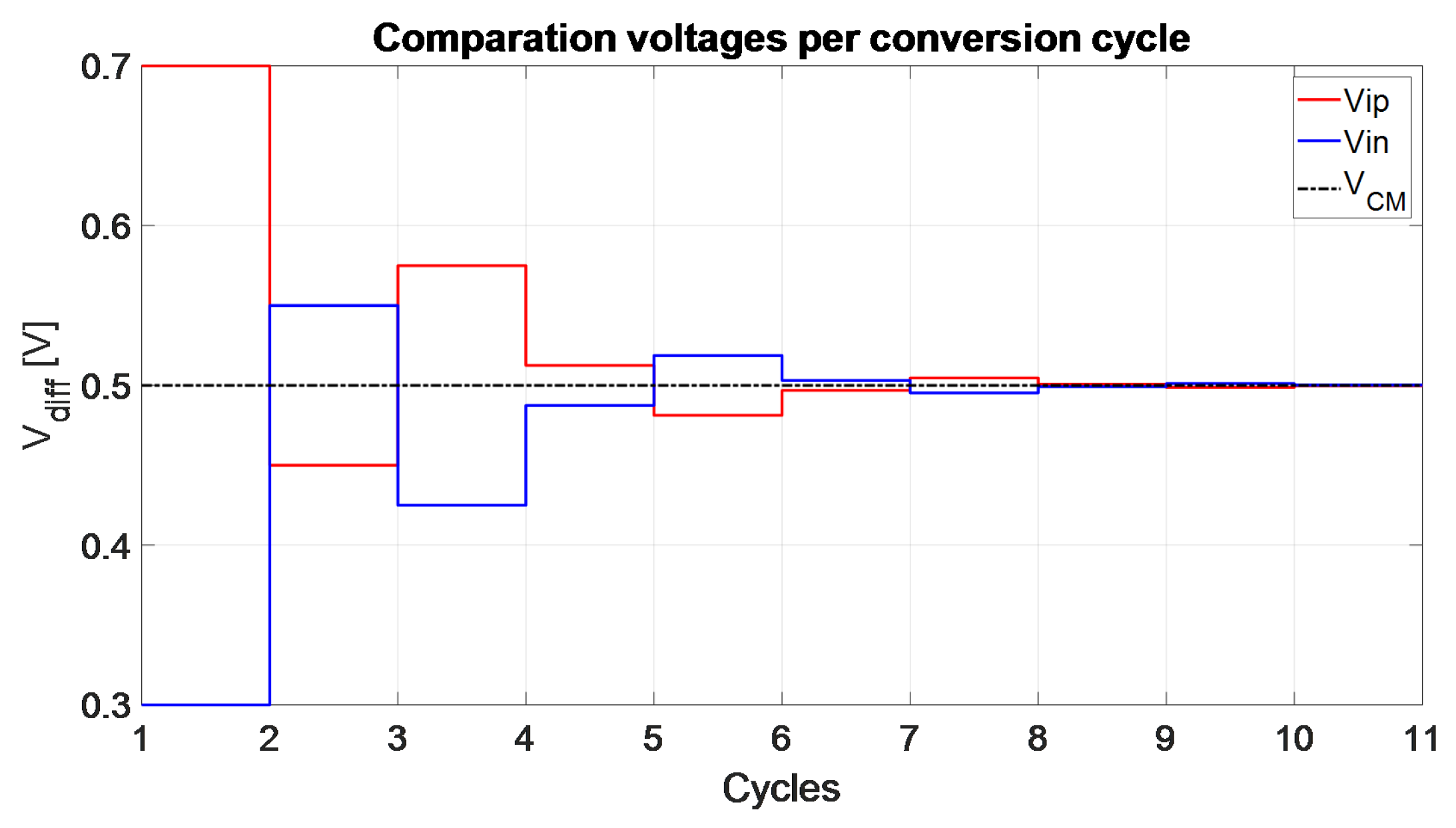
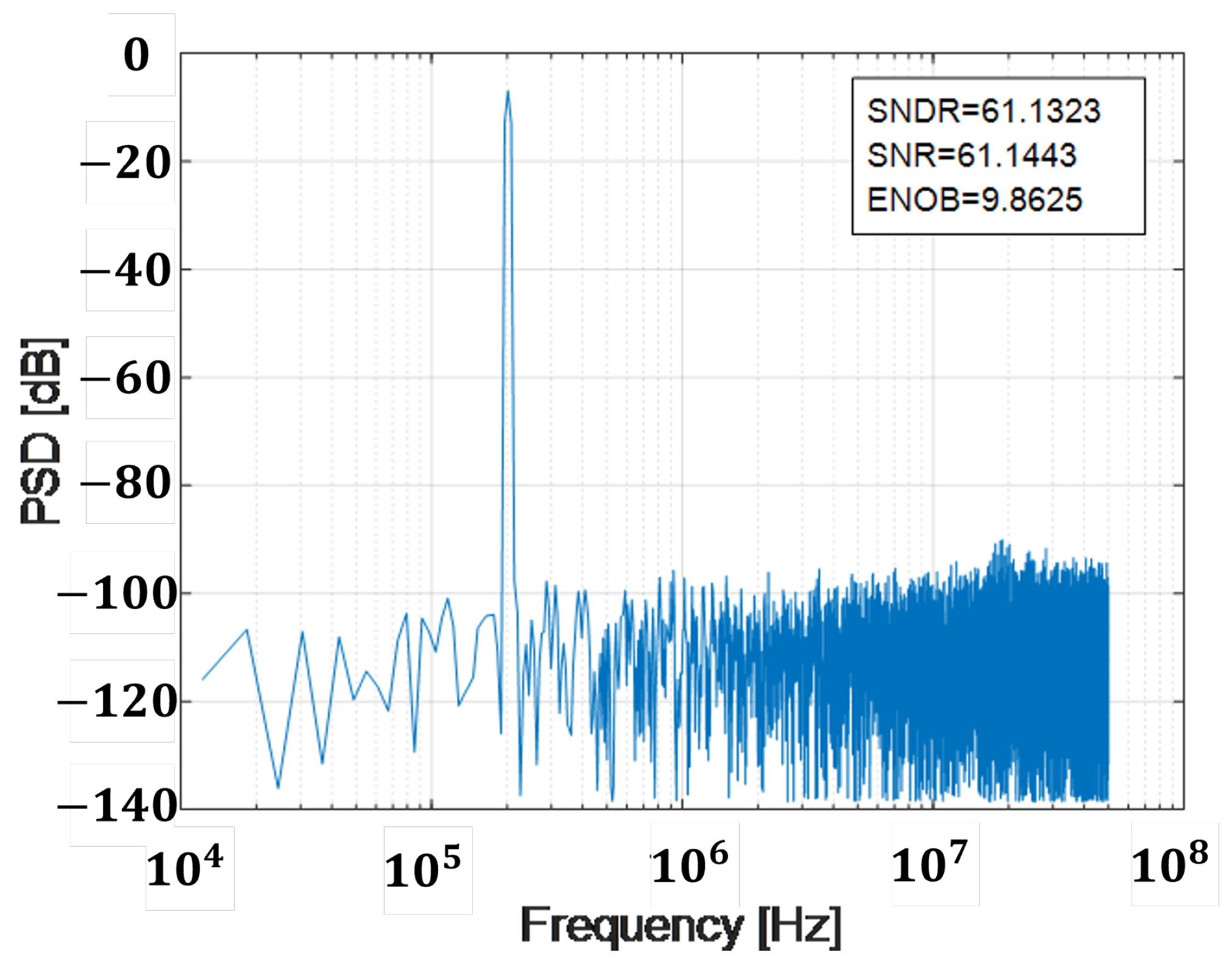
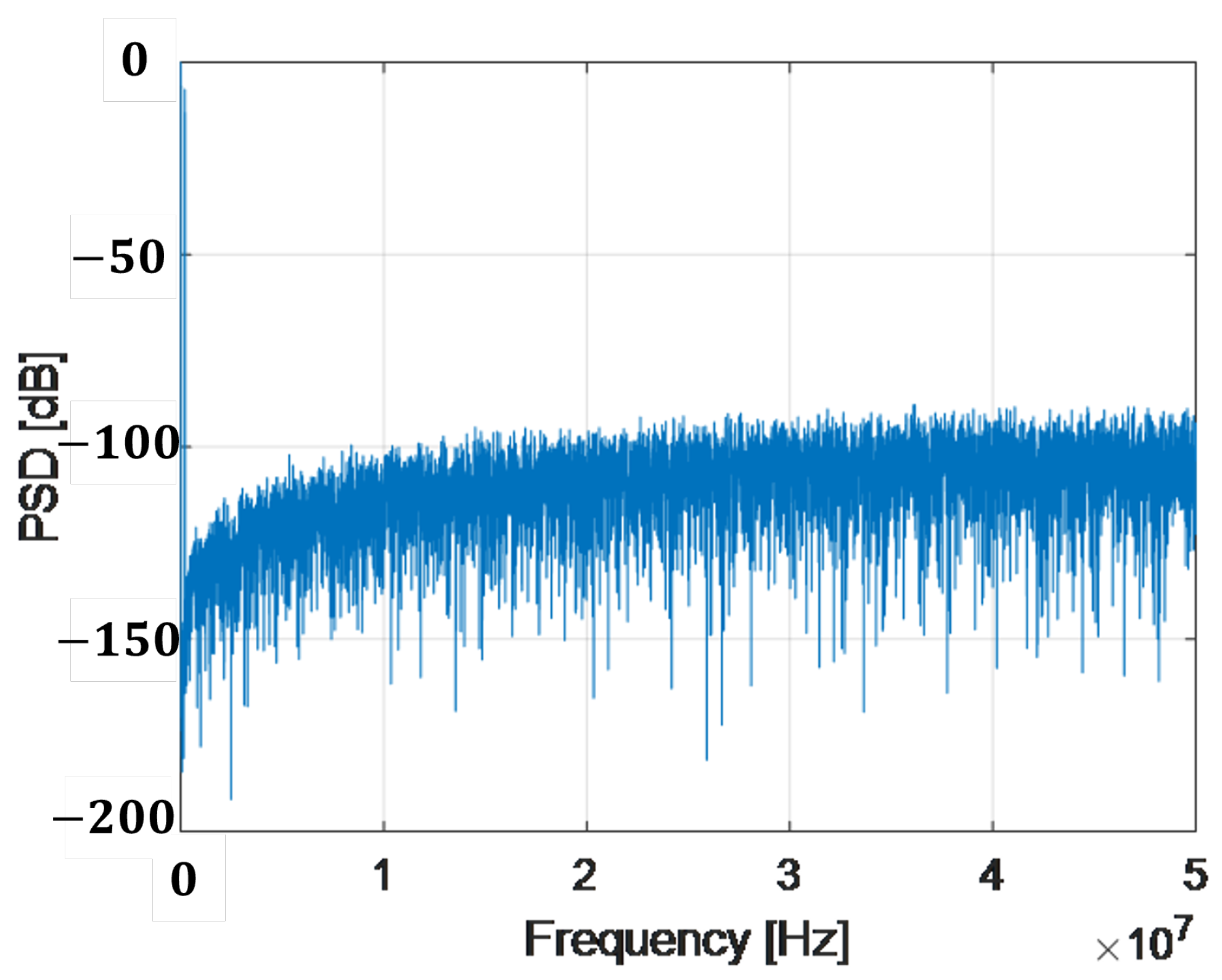
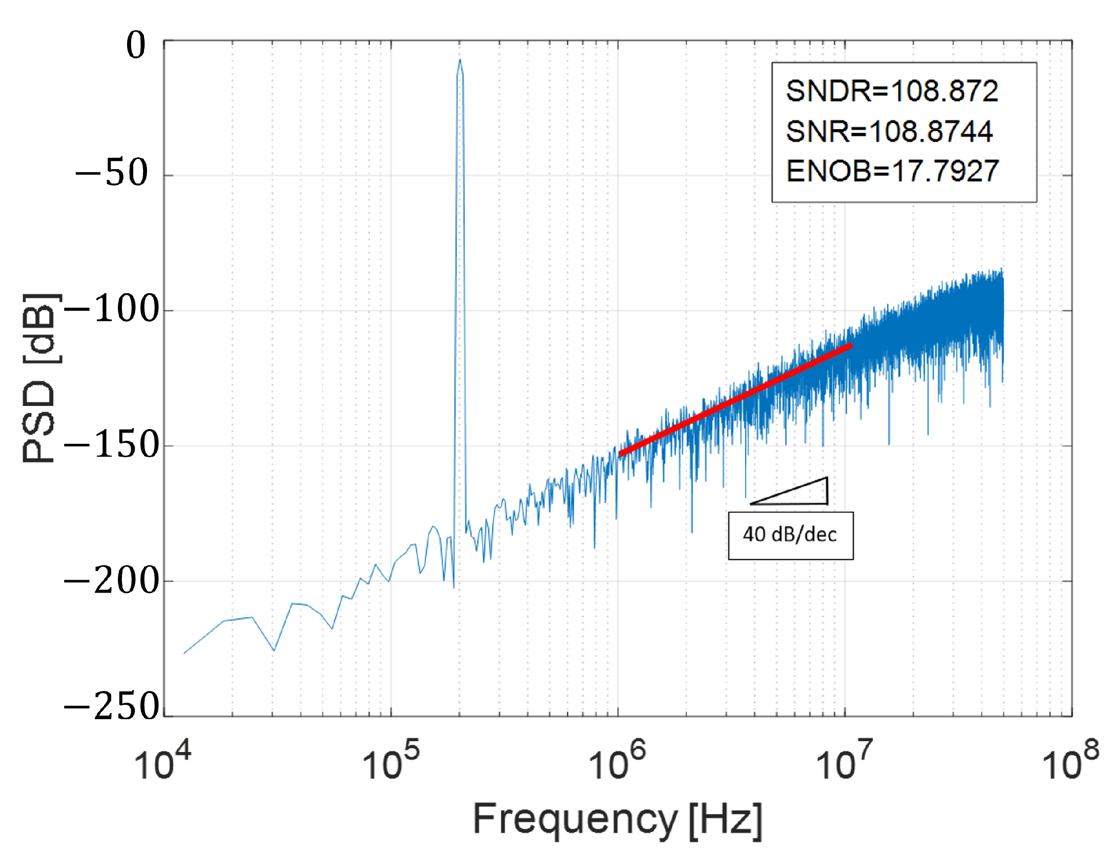
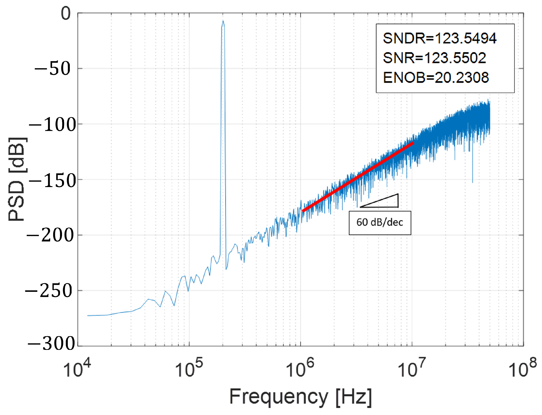
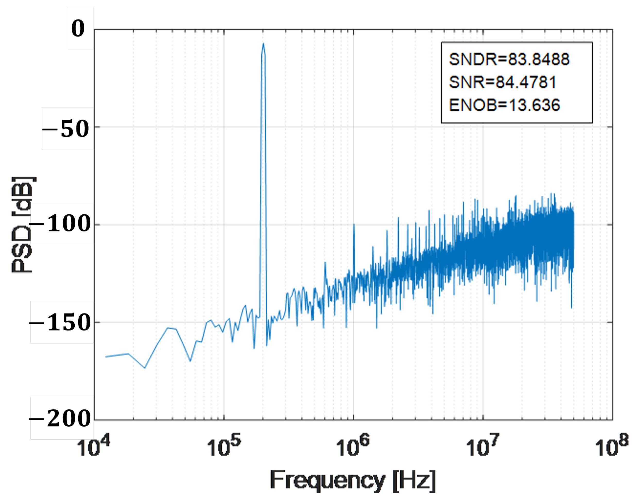
2.2. Noise-Shaping Plots
3. Non-Idealities in the Performance of NS SAR ADC: Problems, Challenges and Solutions
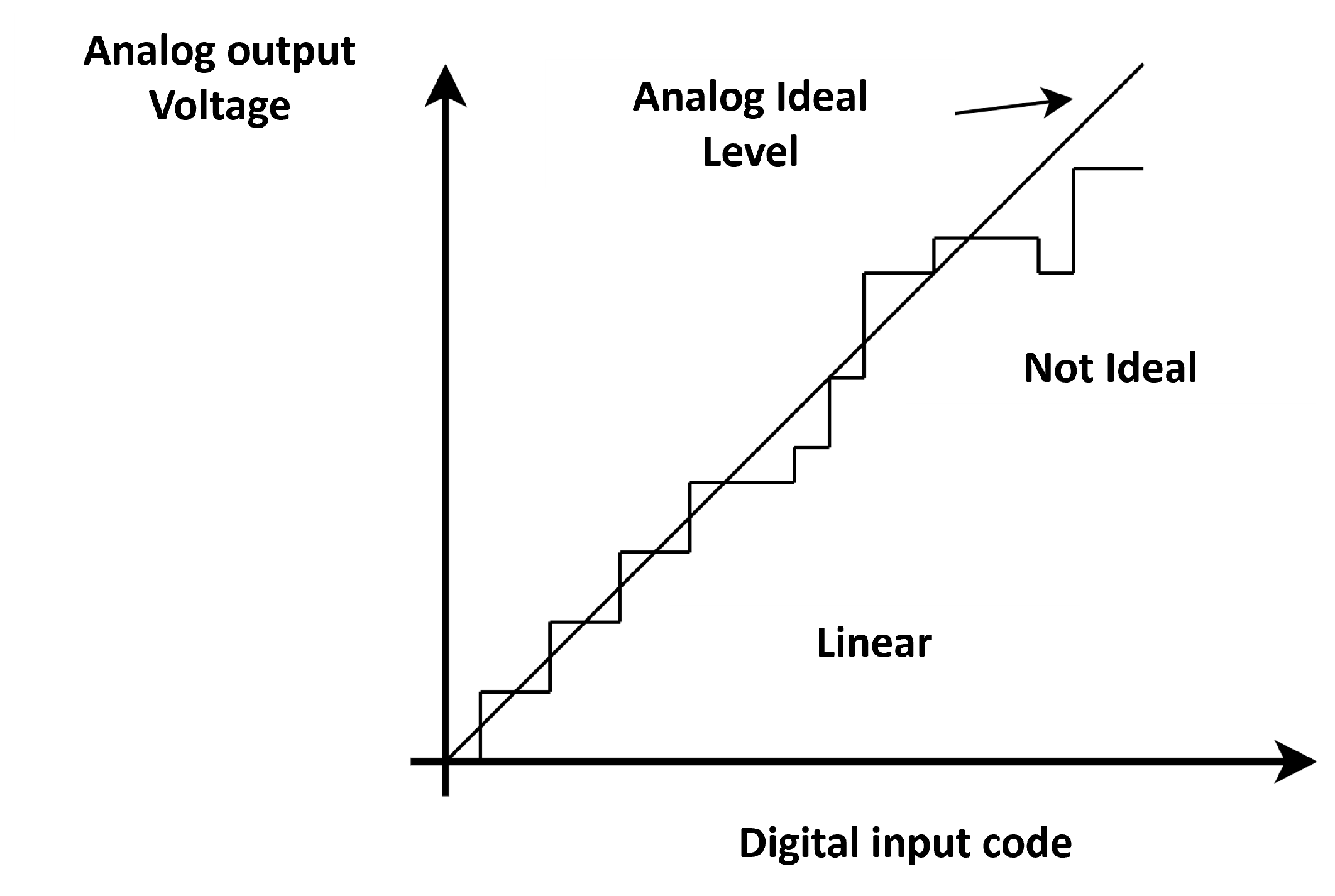
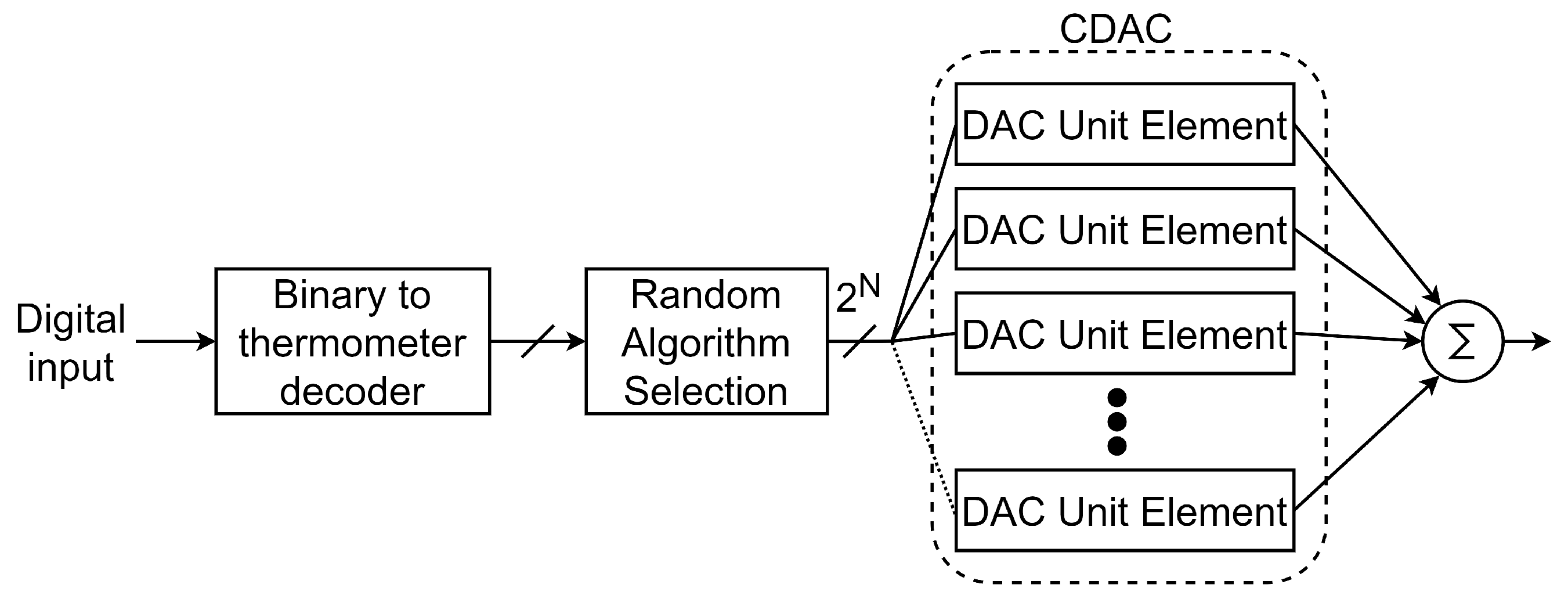
3.1. Mismatch in CDAC
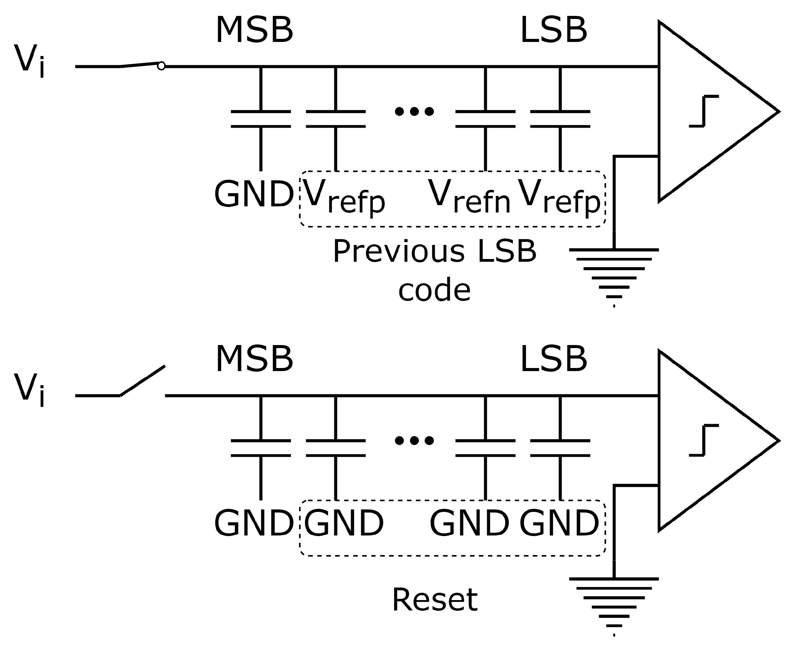
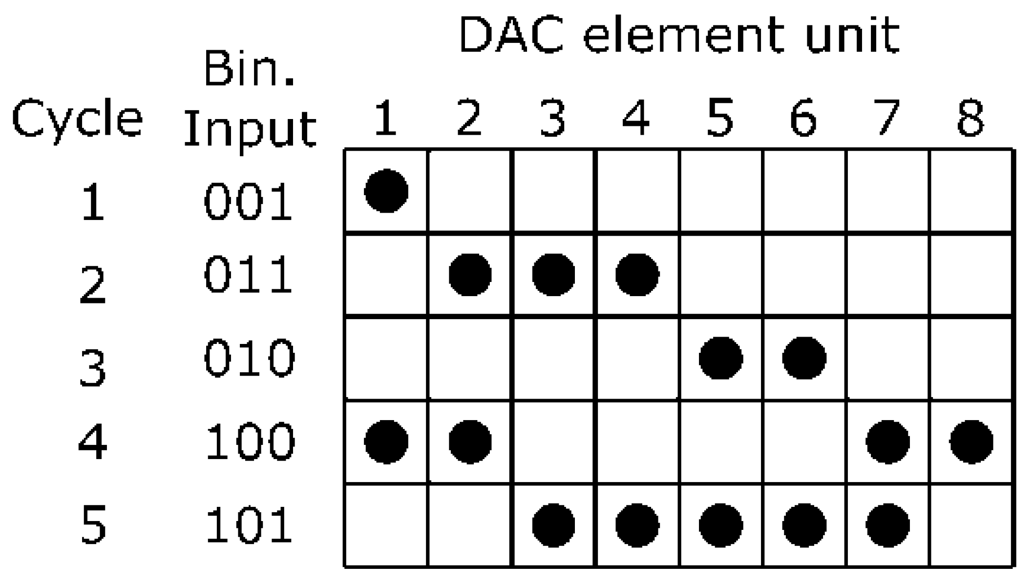
3.2. CDAC Mismatch Correction, an Alternative: NS DEM
3.3. CDAC Mismatch Correction, an Alternative: NS DEM
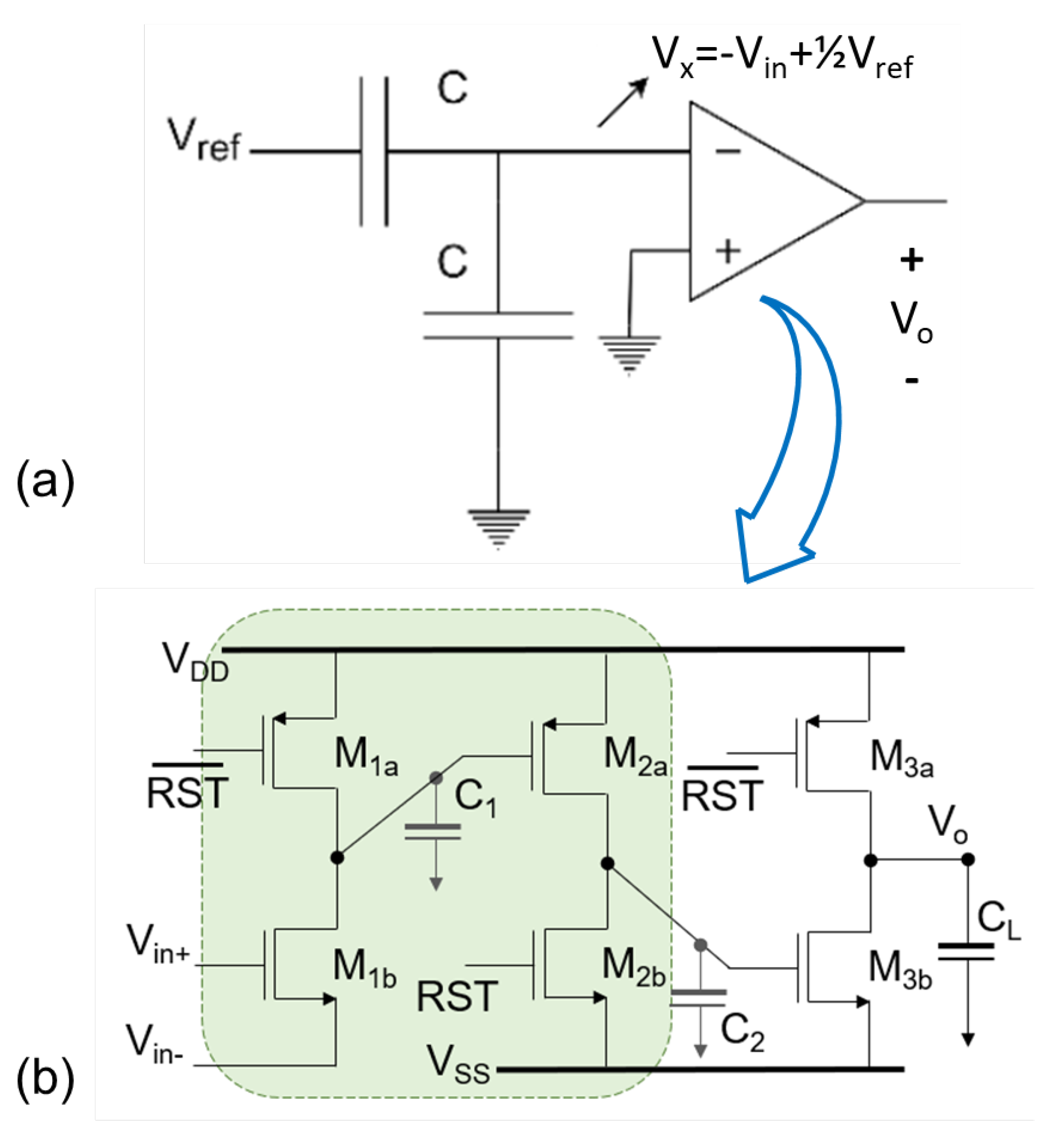
4. Trends on Dynamic Comparison
4.1. CMOS Comparators
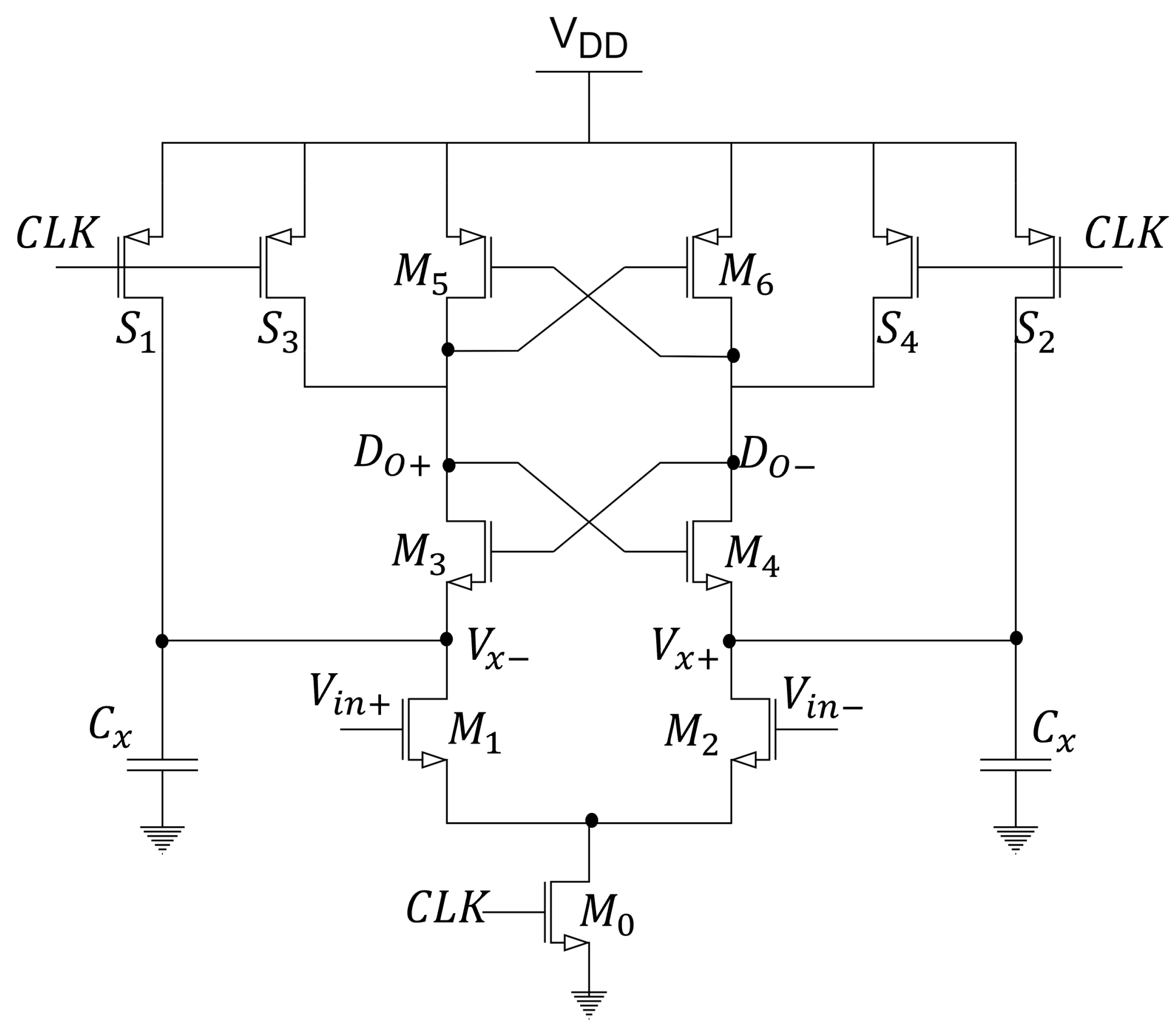
4.2. StrongARM Latch
4.3. Double-Tail Comparator
4.4. Dynamic Two-Stage Comparator
4.5. Dynamic Bias Comparator
4.6. FIA-Based Comparator
4.7. Low-Power Comparator
5. Trends, Further Advances, and Conclusions
Author Contributions
Funding
Institutional Review Board Statement
Informed Consent Statement
Data Availability Statement
Acknowledgments
Conflicts of Interest
References
- Choi, C.; Lee, J.-W. An 11.8-fJ/Conversion-Step Noise Shaping SAR ADC with Embedded Passive Gain for Energy-Efficient IoT Sensors. Sensors 2022, 22, 869. [Google Scholar] [CrossRef] [PubMed]
- Chen, D.; Cui, X.; Zhang, Q.; Li, D.; Cheng, W.; Fei, C.; Yang, Y. A Survey on Analog-to-Digital Converter Integrated Circuits for Miniaturized High Resolution Ultrasonic Imaging System. Micromachines 2022, 13, 114. [Google Scholar] [CrossRef] [PubMed]
- Leene, L.B.; Letchumanan, S.; Constandinou, T.G. A 68μW 31kS/s Fully-Capacitive Noise-Shaping SAR ADC with 102 dB SNDR. In Proceedings of the IEEE International Symposium on Circuits and Systems (ISCAS), Sapporo, Japan, 26–29 May 2019; pp. 1–5. [Google Scholar]
- Lu, R.; Flynn, M.P. A 300MHz-BW 38mW 37dB/40dB SNDR/DR Frequency-Interleaving Continuous-Time Bandpass Delta-Sigma ADC in 28 nm CMOS. In Proceedings of the Symposium on VLSI Circuits, Kyoto, Japan, 13–19 June 2021; pp. 1–2. [Google Scholar]
- Bolatkale, M.; Breems, L.J.; Rutten, R.; Makinwa, K.A.A. A 4GHz CT ΔΣ ADC with 70dB DR and −74dBFS THD in 125MHz BW. In Proceedings of the International Solid-State Circuits Conference, San Francisco, CA, USA, 20–24 February 2011; pp. 470–472. [Google Scholar]
- Ginsburg, B.P.; Chandrakasan, A.P. Highly Interleaved 5b 250MS/s ADC with Redundant Channels in 65nm CMOS. In Proceedings of the International Solid-State Circuits Conference—Digest of Technical Papers, San Francisco, CA, USA, 3–7 February 2008; pp. 240–610. [Google Scholar]
- Kull, L.; Luu, D.; Menolfi, C.; Morf, T.; Francese, P.A.; Braendli, M.; Kossel, M.; Cavrero, A.; Ozkaya, I.; Toifl, T. A 10-Bit 20–40 GS/S ADC with 37 dB SNDR at 40 GHz Input Using First Order Sampling Bandwidth Calibration. In Proceedings of the Symposium on VLSI Circuits, Honolulu, HI, USA, 18–22 June 2018; pp. 275–276. [Google Scholar]
- Zheng, Z.; Wei, L.; Lagos, J.; Martens, E.; Zhu, Y.; Chan, C.-H.; Craninckx, J.; Martins, R.P. 16.3 A Single-Channel 5.5 mW 3.3GS/s 6b Fully Dynamic Pipelined ADC with Post-Amplification Residue Generation. In Proceedings of the IEEE International Solid-State Circuits Conference (ISSCC), San Francisco, CA, USA, 16–20 February 2020; pp. 254–256. [Google Scholar]
- ADC Performance Survey 1997–2021. Available online: http://web.stanford.edu/~murmann/adcsurvey.html (accessed on 22 March 2022).
- Lin, Y.-Z.; Lin, C.-Y.; Tsou, S.-C.; Tsai, C.-H.; Lu, C.-H. 20.2 A 40MHz-BW 320MS/s Passive Noise-Shaping SAR ADC with Passive Signal-Residue Summation in 14nm FinFET. In Proceedings of the IEEE International Solid-State Circuits Conference (ISSCC), San Francisco, CA, USA, 17–21 February 2019; pp. 330–332. [Google Scholar]
- Salgado, G.M.; O’Hare, D.; O’Connell, I. Recent Advances and Trends in Noise Shaping SAR ADCs. IEEE Trans. Circuits Syst. II Express Briefs 2021, 68, 545–549. [Google Scholar] [CrossRef]
- Jie, L.; Tang, X.; Liu, J.; Shen, L.; Li, S.; Sun, N.; Flynn, M. An Overview of Noise-Shaping SAR ADC: From Fundamentals to the Frontier. IEEE Open J. SSCS 2021, 1, 149–161. [Google Scholar] [CrossRef]
- Chen, Z.; Miyahara, M.; Matsuzawa, A. A 9.35-ENOB, 14.8 fJ/conv.-step fully-passive noise-shaping SAR ADC. In Proceedings of the Symposium on VLSI Circuits, Kyoto, Japan, 17–19 June 2015; pp. C64–C65. [Google Scholar]
- Yi, P.; Zhu, Z.; Xu, N.; Fang, L.; Hao, Y. A Unity-Gain Buffer Assisted Noise-Shaping SAR ADC Based on Error-Feedback Structure. Chin. J. Electron. 2022, 31, 658–664. [Google Scholar] [CrossRef]
- Yi, P.; Liang, Y.; Liu, S.; Xu, N.; Fang, L.; Hao, Y. A 625kHz-BW, 79.3dB-SNDR Second-Order Noise-Shaping SAR ADC Using High-Efficiency Error-Feedback Structure. IEEE Trans. Circuits Syst. II Express Briefs 2022, 69, 859–863. [Google Scholar] [CrossRef]
- Li, H.; Shen, Y.; Xin, H.; Cantatore, E.; Harpe, P. A 7.3-μW 13-ENOB 98-dB SFDR Noise-Shaping SAR ADC with Duty-Cycled Amplifier and Mismatch Error Shaping. J. Solid-State Circuits 2022, 57, 2078–2089. [Google Scholar] [CrossRef]
- Li, S.; Qiao, B.; Gandara, M.; Pan, D.Z.; Sun, N. A 13-ENOB Second-Order Noise-Shaping SAR ADC Realizing Optimized NTF Zeros Using the Error-Feedback Structure. IEEE J. Solid-State Circuits 2018, 53, 3484–3496. [Google Scholar] [CrossRef]
- Fredenburg, J.; Flynn, M. A 90MS/s 11MHz bandwidth 62dB SNDR noise-shaping SAR ADC. IEEE Int. Solid-State Circuits Conf. 2012, 47, 468–470. [Google Scholar]
- Li, S.; Liu, J.; Guo, W.; Sun, N. Chapter 2: Noise-Shaping SAR ADCs. In Next-Generation ADCs, High-Performance Power Management, and Technology Considerations for Advanced Integrated Circuits, Advances in Analog Circuit Design 2019; Baschirotto, A., Harpe, P., Makinwa, K., Eds.; Springer: Cham, Switzerland, 2020; pp. 21–40. [Google Scholar]
- Shu, Y.-S.; Kuo, L.-T.; Lo, T.-Y. An Oversampling SAR ADC with DAC Mismatch Error Shaping Achieving 105 dB SFDR and 101 dB SNDR Over 1 kHz BW in 55 nm CMOS. J. Solid-State Circuits 2016, 51, 2928–2940. [Google Scholar] [CrossRef]
- Obata, K.; Matsukawa, K.; Miki, T.; Tsukamoto, Y.; Sushihara, K. A 97.99 dB SNDR, 2 kHz BW, 37.1 µW noise-shaping SAR ADC with dynamic element matching and modulation dither effect. In Proceedings of the Symposium on VLSI Circuits, Honolulu, HI, USA, 15–17 June 2016; pp. 1–2. [Google Scholar]
- Zhang, Y.; Liu, S.; Tian, B.; Zhu, Y.; Chan, C.-H.; Zhu, Z. A 2nd-Order Noise-Shaping SAR ADC with Lossless Dynamic Amplifier Assisted Integrator. Trans. Circuits Syst. II Express Briefs 2020, 67, 1819–1823. [Google Scholar] [CrossRef]
- Liu, J.; Wang, X.; Gao, Z.; Zhan, M.; Tang, X.; Sun, N. 9.3 A 40kHz-BW 90dB-SNDR Noise-Shaping SAR with 4× Passive Gain and 2nd-Order Mismatch Error Shaping. In Proceedings of the International Solid-State Circuits Conference, San Francisco, CA, USA, 16–20 February 2020; pp. 158–160. [Google Scholar]
- Zhuang, H.; Guo, W.; Liu, J.; Tang, H.; Zhu, Z.; Chen, L.; Sun, N. A Second-Order Noise-Shaping SAR ADC with Passive Integrator and Tri-Level Voting. J. Solid-State Circuits 2019, 54, 1636–1647. [Google Scholar] [CrossRef]
- Kim, T.; Chae, Y. A 2MHz BW Buffer-Embedded Noise-Shaping SAR ADC Achieving 73.8dB SNDR and 87.3dB SFDR. In Proceedings of the Custom Integrated Circuits Conference, Austin, TX, USA, 15–17 April 2019; pp. 1–4. [Google Scholar]
- Hernes, B.; Bjornsen, J.; Andersen, T.N.; Vinje, A.; Korsvoll, H.; Telsto, F.; Briskemyr, A.; Holdo, C.; Moldsvor, O. A 92.5mW 205MS/s 10b Pipeline IF ADC Implemented in 1.2V/3.3V 0.13μm CMOS. In Proceedings of the International Solid-State Circuits Conference. Digest of Technical Papers, San Francisco, CA, USA, 11–15 February 2007; pp. 462–615. [Google Scholar]
- Zhang, Q.; Ning, N.; Li, J.; Yu, Q.; Wu, K.; Zhang, Z. A Second-Order Noise-Shaping SAR ADC Using Two Passive Integrators Separated by the Comparator. Trans. Very Large Scale Integr. (VLSI) Syst. 2021, 29, 227–231. [Google Scholar] [CrossRef]
- Garvik, H.; Wulff, C.; Ytterdal, T. An 11.0 bit ENOB, 9.8 fJ/conv.-step noise-shaping SAR ADC calibrated by least squares estimation. In Proceedings of the IEEE Custom Integrated Circuits Conference (CICC), Austin, TX, USA, 30 April–3 May 2017; pp. 1–4. [Google Scholar]
- Tang, X.; Yang, X.; Zhao, W.; Hsu, C.; Liu, J.; Shen, L.; Mukherjee, A.; Shi, W.; Pna, D.; Sun, N. A 13.5-ENOB, 107-μW noise-shaping SAR ADC with PVT-robust closed-loop dynamic amplifier. IEEE J. Solid-State Circuits 2020, 55, 3248–3259. [Google Scholar] [CrossRef]
- Lim, Y.; Flynn, M.P. 26.1 A 1mW 71.5dB SNDR 50MS/S 13b fully differential ring-amplifier-based SAR-assisted pipeline ADC. In Proceedings of the International Solid-State Circuits Conference Digest of Technical Papers, San Francisco, CA, USA, 22–26 February 2015; pp. 1–3. [Google Scholar]
- Jie, L.; Zheng, B.; Chen, H.-W.; Wang, R.; Flynn, M.P. 9.4 A 4th-Order Cascaded-Noise-Shaping SAR ADC with 88dB SNDR over 100kHz Bandwidth. In Proceedings of the IEEE International Solid-State Circuits Conference, San Francisco, CA, USA, 16–20 February 2020; pp. 160–162. [Google Scholar]
- Wang, T.-H.; Wu, R.; Gupta, V.; Li, S. 27.3 A 13.8-ENOB 0.4pF-CIN 3rd-Order Noise-Shaping SAR in a Single-Amplifier EF-CIFF Structure with Fully Dynamic Hardware-Reusing kT/C Noise Cancelation. In Proceedings of the IEEE International Solid-State Circuits Conference (ISSCC), San Francisco, CA, USA, 13–22 February 2021; pp. 374–376. [Google Scholar]
- Zhang, Q.; Ning, N.; Zhang, Z.; Li, J.; Wu, K.; Chen, Y.; Yu, Q. A 13-Bit ENOB Third-Order Noise-Shaping SAR ADC Employing Hybrid Error Control Structure and LMS-Based Foreground Digital Calibration. IEEE J. Solid-State Circuits 2022, 57, 2181–2195. [Google Scholar] [CrossRef]
- Wang, T.; Xie, T.; Liu, Z.; Li, S. An 84dB-SNDR Low-OSR 4th-Order Noise-Shaping SAR with an FIA-Assisted EF-CRFF Structure and Noise-Mitigated Push-Pull Buffer-in-Loop Technique. In Proceedings of the IEEE International Solid-State Circuits Conference (ISSCC), San Francisco, CA, USA, 20–26 February 2022; pp. 418–420. [Google Scholar]
- Fu, X.; El-Sankary, K. A 14.5-Bit ENOB, 10MS/s SAR-ADC with 2nd Order Hybrid Passive-Active Resonator Noise Shaping. IEEE Access 2022, 10, 54589–54598. [Google Scholar] [CrossRef]
- Salgado, G.M.; O’Hare, D.; O’Connell, I. Modeling and Analysis of Error Feedback Noise-Shaping SAR ADCs. In Proceedings of the IEEE International Symposium on Circuits and Systems (ISCAS), Seville, Spain, 12–24 October 2020; pp. 1–5. [Google Scholar]
- Jiao, Z.; Chen, Y.; Su, X.; Sun, Q.; Wang, X.; Zhang, R.; Zhang, H. A Configurable Noise-Shaping Band-Pass SAR ADC with Two-Stage Clock-Controlled Amplifier. IEEE Trans. Circuits Syst. I Regul. Pap. 2020, 67, 3728–3739. [Google Scholar] [CrossRef]
- McNeill, J.A.; Chan, K.Y.; Coln, M.C.W.; David, C.L.; Brenneman, C. All-Digital Background Calibration of a Successive Approximation ADC Using the “Split ADC” Architecture. Trans. Circuits Syst. I Regul. Pap. 2011, 58, 2355–2365. [Google Scholar] [CrossRef]
- Liu, J.; Li, D.; Zhong, Y.; Tang, X.; Sun, N. 27.1 A 250kHz-BW 93dB-SNDR 4th-Order Noise-Shaping SAR Using Capacitor Stacking and Dynamic Buffering. In Proceedings of the IEEE International Solid-State Circuits Conference (ISSCC), San Francisco, CA, USA, 13–22 February 2021; pp. 369–371. [Google Scholar]
- Yang, C.; Qiu, L.; Tang, K.; Zheng, Y. A 98.6 dB SNDR SAR ADC with a Mismatch Error Shaping Technique Implemented with Double Sampling. Trans. Circuits Syst. II Express Briefs 2022, 69, 774–778. [Google Scholar] [CrossRef]
- Li, H.; Shen, Y.; Xin, H.; Cantatore, E.; Harpe, P. An 80dB-SNDR 98dB-SFDR Noise-Shaping SAR ADC with Duty-Cycled Amplifier and Digital-Predicted Mismatch Error Shaping. Eur. Solid State Circuits Conf. 2021, 47, 387–390. [Google Scholar]
- Liu, J.; Hsu, C.-K.; Tang, X.; Li, S.; Wen, G.; Sun, N. Error-Feedback Mismatch Error Shaping for High-Resolution Data Converters. Trans. Circuits Syst. I Regul. Pap. 2019, 66, 1342–1354. [Google Scholar] [CrossRef]
- Shen, Y.; Li, H.; Xin, H.; Cantatore, E.; Harpe, P. A 103-dB SFDR Calibration-Free Oversampled SAR ADC with Mismatch Error Shaping and Pre-Comparison Techniques. J. Solid-State Circuits 2022, 57, 734–744. [Google Scholar] [CrossRef]
- Neitola, M.; Rahkonen, T. A Generalized Data-Weighted Averaging Algorithm. Trans. Circuits Syst. II Express Briefs 2010, 57, 115–119. [Google Scholar] [CrossRef]
- Analísis y Diseño de un Sistema de Corrección dináMica híBrida para un Modulador Sigma Delta Multi-Bit Pasa-Banda. Available online: https://repositorioinstitucional.uabc.mx/handle/20.500.12930/2144 (accessed on 14 May 2023).
- Hasebe, K.; Etou, S.; Miyazaki, D.; Iguchi, T.; Yagishita, Y.; Takasaki, M.; Nogomida, T.; Watanabe, H.; Matsumoto, T.; Katayama, Y. A 100kHz-Bandwidth 98.3dB-SNDR Noise-Shaping SAR ADC with Improved Mismatch Error Shaping and Speed-Up Techniques. In Proceedings of the IEEE Symposium on VLSI Technology and Circuits, Honolulu, HI, USA, 12–17 June 2022; pp. 56–57. [Google Scholar]
- Jie, L.; Zheng, B.; Chen, H.-W.; Flynn, M.P. A Cascaded Noise-Shaping SAR Architecture for Robust Order Extension. J. Solid-State Circuits 2020, 55, 3236–3247. [Google Scholar] [CrossRef]
- Miyahara, M.; Matsuzawa, A. An 84 dB dynamic range 62.5–625 kHz bandwidth clock-scalable noise-shaping SAR ADC with open-loop integrator using dynamic amplifier. In Proceedings of the IEEE Custom Integrated Circuits Conference (CICC), Austin, TX, USA, 30 April–3 May 2017; pp. 1–4. [Google Scholar]
- Liu, C.-C.; Huang, M.-C. 28.1 A 0.46mW 5MHz-BW 79.7dB-SNDR noise-shaping SAR ADC with dynamic-amplifier-based FIR-IIR filter. In Proceedings of the International Solid-State Circuits Conference, San Francisco, CA, USA, 5–9 February 2017; pp. 466–467. [Google Scholar]
- Zhang, Q.; Li, J.; Ning, N.; Yu, Q.; Wu, K.; Zhang, Z. A second-order noise-shaping SAR ADC with error-feedback structure and data weighted averaging. Microelectron. J. 2020, 105, 104–905. [Google Scholar] [CrossRef]
- Chen, J.; Xu, Y.P. A novel noise-shaping DAC for multi-bit sigma-delta modulator. Trans. Circuits Syst. II Express Briefs 2006, 53, 344–348. [Google Scholar] [CrossRef]
- Guo, Y.; Jin, J.; Liu, X.; Zhou, J. A 60-MS/s 5-MHz BW Noise-Shaping SAR ADC with Integrated Input Buffer Achieving 84.2-dB SNDR and 97.3-dB SFDR Using Dynamic Level-Shifting and ISI-Error Correction. J. Solid-State Circuits 2022, 58, 474–485. [Google Scholar] [CrossRef]
- Kapusta, R.; Zhu, H.; Lyden, C. Sampling circuits that break the kT/C thermal noise limit. In Proceedings of the IEEE 2013 Custom Integrated Circuits Conference, San Jose, CA, USA, 22–25 September 2013; pp. 1–6. [Google Scholar]
- Abo, A.M.; Gray, P.R. A 1.5-V, 10-bit, 14.3-MS/s CMOS pipeline analog-to-digital converter. J. Solid-State Circuits 1999, 34, 599–606. [Google Scholar] [CrossRef]
- Cho, T.B.; Gray, P.R. A 10 b, 20 Msample/s, 35 mW pipeline A/D converter. J. Solid-State Circuits 1995, 30, 166–172. [Google Scholar] [CrossRef]
- Sanduleanu, M.A.T.; Tuijl, A.J.M. Chopping: A technique for noise and offset reduction. In Power Trade-Offs and Low Power in Analog CMOS ICs; Kluwer Academic Publishers: New York, NY, USA, 2002; Chapter 5; pp. 101–125. [Google Scholar]
- Zheng, Y. An overview in dynamic comparators optimization methods. In Proceedings of the 4th International Conference on Electronic Engineering and Informatics, Guiyang, China, 24–26 June 2022; pp. 1–10. [Google Scholar]
- Chevella, S.; O’Hare, D.; O’Connell, I. A low-power 1-v supply dynamic comparator. IEEE Solid-State Circuits Lett. 2020, 3, 154–157. [Google Scholar] [CrossRef]
- van Elzakker, M.; van Tuijl, E.; Geraedts, P.; Schinkel, D.; Klumperink, E.A.M.; Nauta, B. A 10-bit charge-redistribution adc consuming 1.9 μw at 1 ms/s. IEEE J. Solid-State Circuits 2010, 45, 1007–1015. [Google Scholar] [CrossRef]
- Liu, M.; Pelzers, K.; van Dommele, R.; van Roermund, A.; Harpe, P. A 106nw 10 b 80 ks/s sar adc with duty-cycled reference generation in 65 nm cmos. IEEE J. Solid-State Circuits 2016, 51, 2435–2445. [Google Scholar] [CrossRef]
- Harpe, P.; Cantatore, E.; van Roermund, A. A 2.2/2.7fj/conversion- step 10/12b 40ks/s sar adc with data-driven noise reduction. In Proceedings of the IEEE International Solid-State Circuits Conference Digest of Technical Papers, San Francisco, CA, USA, 17–21 February 2013; pp. 270–271. [Google Scholar]
- Jendernalik, W. An Ultra-Low-Energy Analog Comparator for A/D Converters in CMOS Image Sensors. Circuits Syst. Signal Process 2017, 36, 4829–4843. [Google Scholar] [CrossRef]
- Razavi, B. The strongarm latch [a circuit for all seasons]. IEEE Solid-State Circuits Mag. 2015, 7, 12–17. [Google Scholar] [CrossRef]
- Schinkel, D.; Mensink, E.; Klumperink, E.; van Tuijl, E.; Nauta, B. A double-tail latch-type voltage sense amplifier with 18ps setup+hold time. In Proceedings of the IEEE International Solid-State Circuits Conference, San Francisco, CA, USA, 11–15 February 2007; pp. 314–605. [Google Scholar]
- Babayan-Mashhadi, S.; Lotfi, R. Analysis and design of a low voltage low-power double-tail comparator. IEEE Trans. Very Large Scale Integr. (VLSI) Syst. 2014, 22, 343–352. [Google Scholar] [CrossRef]
- Bindra, H.S.; Lokin, C.E.; Schinkel, D.; Annema, A.-J.; Nauta, B. A 1.2-v dynamic bias latch-type comparator in 65-nm cmos with 0.4-mv input noise. IEEE J. Solid-State Circuits 2018, 53, 1902–1912. [Google Scholar] [CrossRef]
- Tang, X.; Shen, L.; Kasap, B.; Yang, X.; Shi, W.; Mukherjee, A.; Pan, D.Z.; Sun, N. An energy-efficient comparator with dynamic floating inverter amplifier. IEEE J. Solid-State Circuits 2020, 55, 1011–1022. [Google Scholar] [CrossRef]
- Li, Z.; He, W.; Ye, F.; Ren, J. A low-power low-noise dynamic comparator with latch-embedding floating amplifier. In Proceedings of the IEEE Asia Pacific Conference on Circuits and Systems (APCCAS), Ha Long, Vietnam, 8–10 December 2020; pp. 39–42. [Google Scholar]
- Jie, L.; Zheng, B.; Flynn, M.P. 20.3 A 50MHz-Bandwidth 70.4dB-SNDR Calibration-Free Time-Interleaved 4th-Order Noise-Shaping SAR ADC. In Proceedings of the International Solid-State Circuits Conference, San Francisco, CA, USA, 17–21 February 2019; pp. 332–334. [Google Scholar]
- Liu, J.; Li, S.; Guo, W.; Wen, G.; Sun, N. A 0.029-mm2 17-fJ/Conversion-Step Third-Order CT ΔΣ ADC with a Single OTA and Second-Order Noise-Shaping SAR Quantizer. J. Solid-State Circuits 2019, 54, 428–440. [Google Scholar] [CrossRef]
- Akbari, M.; Honarparvar, M.; Savaria, Y.; Sawan, M. OTA-Free MASH 2–2 Noise Shaping SAR ADC: System and Design Considerations. In Proceedings of the International Symposium on Circuits and Systems, Seville, Spain, 12–14 October 2020; pp. 1–5. [Google Scholar]
- Lin, Y.-S.; Chang, S.-J.; Wei, C.-L. A Noise-shaping SAR Assisted MASH 2-1 Sigma-Delta Modulator. In Proceedings of the International Symposium on VLSI Design, Automation and Test (VLSI-DAT), Hsinchu, Taiwan, 10–13 August 2020; pp. 1–4. [Google Scholar]
- Oh, S.; Oh, Y.; Lee, J.; Kim, K.; Lee, S.; Kim, J.; Chae, H. A 80dB DR 6MHz Bandwidth Pipelined Noise-Shaping SAR ADC with 1–2 MASH structure. In Proceedings of the Custom Integrated Circuits Conference, Boston, MA, USA, 22–25 March 2020; pp. 1–4. [Google Scholar]
- Gao, B.; Li, X.; Yan, C.; Wu, J. Active Noise Shaping SAR ADC Based on ISDM with the 5MHz Bandwidth. In Proceedings of the International Symposium on Circuits and Systems, Seville, Spain, 12–14 October 2020; pp. 1–4. [Google Scholar]
- Bajaj, V.; Kannan, A.; Paul, M.E.; Krishnapura, N. Noise Shaping Techniques for SNR Enhancement in SAR Analog to Digital Converters. In Proceedings of the International Symposium on Circuits and Systems, Seville, Spain, 12–14 October 2020; pp. 1–5. [Google Scholar]


| Specification | Lu 2020 [31] | Wang 2021 [32] | Zhang 2022 [33] | Wang 2022 [34] | Fu 2022 [35] |
|---|---|---|---|---|---|
| Filter | Cascade-EF | EF-CIFF | EF-CIFF | EF-CRFF | CRFF |
| Process | 28 nm | 65 nm | 130 nm | 65 nm | 180 nm |
| Order | 4 | 3 | 3 | 4 | 2 |
| Supply | 1 V | 1.1 V | 1.2 V | 2 V | 1.8 V |
| Bits | 10 | 10 | 8 | 10 | 10 |
| BW | 100 kHz | 625 kHz | 125 kHz | 500 kHz | 1 MHz |
| OSR | 10 | 8 | 8 | 5 | - |
| SNDR | 87.6 dB | 84.8 dB | 79.5 dB | 84.1 dB | 89.4 dB |
| Power | 120 µW | 119 µW | 96 µW | 134 µW | 880 µW |
| FoMs | 176.8 dB | 182 dB | 170.7 dB | 182.4 dB | 187.3 |
| Problem | Solutions | Techniques |
|---|---|---|
| Mismatch in DAC | Increment in CDAC area | · Larger DAC unit elements |
| Digital calibration | · Foreground · Background | |
| Digital Mismatch Shaping-Dynamic Element Matching (DEM) | · Data Weighted Averaging (DWA) · Segmented DEM | |
| Mismatch Error Shaping (MES) | · Preset of LSBs | |
| kT/C and flicker noise + offset | Switches and amplifiers designs | · Clock Boosting · Bootstrapping · Buffer design · Chopper modulation |
| Reference | Calibration Technique | SFDR [dB] |
|---|---|---|
| Li 2018 [17] | Background LMS | 89 |
| Zhuang 2019 [24] | Background LMS | 90 |
| Jie 2020 [47] | LUT Foreground | 102.8 |
| Liu 2021 [39] | Foreground | 104.4 |
| Wang 2021 [32] | Foreground LMS | 103 |
| Liu 2019 [42] | MES | 122* |
| Yang 2022 [40] | MES | 104.5 |
| Li 2021 [41] | MES | 98 |
| Shen 2022 [43] | MES | 103 |
| Li 2022 [16] | MES | 98 |
| Obata 2016 [21] | DEM + Dither | 112 |
| Miyahara 2017 [48] | Binary mode DEM | 84.3 |
| CC Liu 2017 [49] | DWA | 92.2 |
| Zhang 2020 [50] | DWA | 97.34 |
| Zhang 2021 [27] | DWA | 92.9 |
| Shu 2016 [20] | MES + DWA | 105.1 |
| Liu 2020 [23] | MES + DWA | 102.2 |
| Hasebe 2022 [46] | MES + DWA | 108.5 |
Disclaimer/Publisher’s Note: The statements, opinions and data contained in all publications are solely those of the individual author(s) and contributor(s) and not of MDPI and/or the editor(s). MDPI and/or the editor(s) disclaim responsibility for any injury to people or property resulting from any ideas, methods, instructions or products referred to in the content. |
© 2024 by the authors. Licensee MDPI, Basel, Switzerland. This article is an open access article distributed under the terms and conditions of the Creative Commons Attribution (CC BY) license (https://creativecommons.org/licenses/by/4.0/).
Share and Cite
Arzate-Palma, V.H.; Rivera-Orozco, D.G.; Molina Salgado, G.; Sandoval-Ibarra, F. A Review on Fundamentals of Noise-Shaping SAR ADCs and Design Considerations. Chips 2024, 3, 153-181. https://doi.org/10.3390/chips3020007
Arzate-Palma VH, Rivera-Orozco DG, Molina Salgado G, Sandoval-Ibarra F. A Review on Fundamentals of Noise-Shaping SAR ADCs and Design Considerations. Chips. 2024; 3(2):153-181. https://doi.org/10.3390/chips3020007
Chicago/Turabian StyleArzate-Palma, Victor H., David G. Rivera-Orozco, Gerardo Molina Salgado, and Federico Sandoval-Ibarra. 2024. "A Review on Fundamentals of Noise-Shaping SAR ADCs and Design Considerations" Chips 3, no. 2: 153-181. https://doi.org/10.3390/chips3020007
APA StyleArzate-Palma, V. H., Rivera-Orozco, D. G., Molina Salgado, G., & Sandoval-Ibarra, F. (2024). A Review on Fundamentals of Noise-Shaping SAR ADCs and Design Considerations. Chips, 3(2), 153-181. https://doi.org/10.3390/chips3020007