1. Introduction
The continuous scaling down of CMOS technologies allows for the integration of enormous high speed digital circuits and advanced analog and radio-frequency (RF) circuits on the same silicon die. Mixed-signal system-on-chips (SoCs) have major advantages including low power consumption, high speed performance, smaller printed circuit board, and low fabrication cost. One of the most crucial obstacles in the SoCs design process and related performance simulation is the noise simulation generated by the high-speed switching of the digital blocks [
1].
Noise margins have been reduced significantly due to the lowering of the power supply and threshold voltages. This leads the sensitive analog/RF circuits to become more susceptible to noise. Furthermore, the demanding operation frequencies are constantly increasing and therefore impose stricter constrains on the time requirements of the critical paths. The higher clock rates results in faster signal transitions, exacerbating the noise margins. In sub-micrometer technologies, the delay induced by interconnects becomes comparable to the delay of the logic gates and the impact of the noise on the system performance impose challenging design approaches.
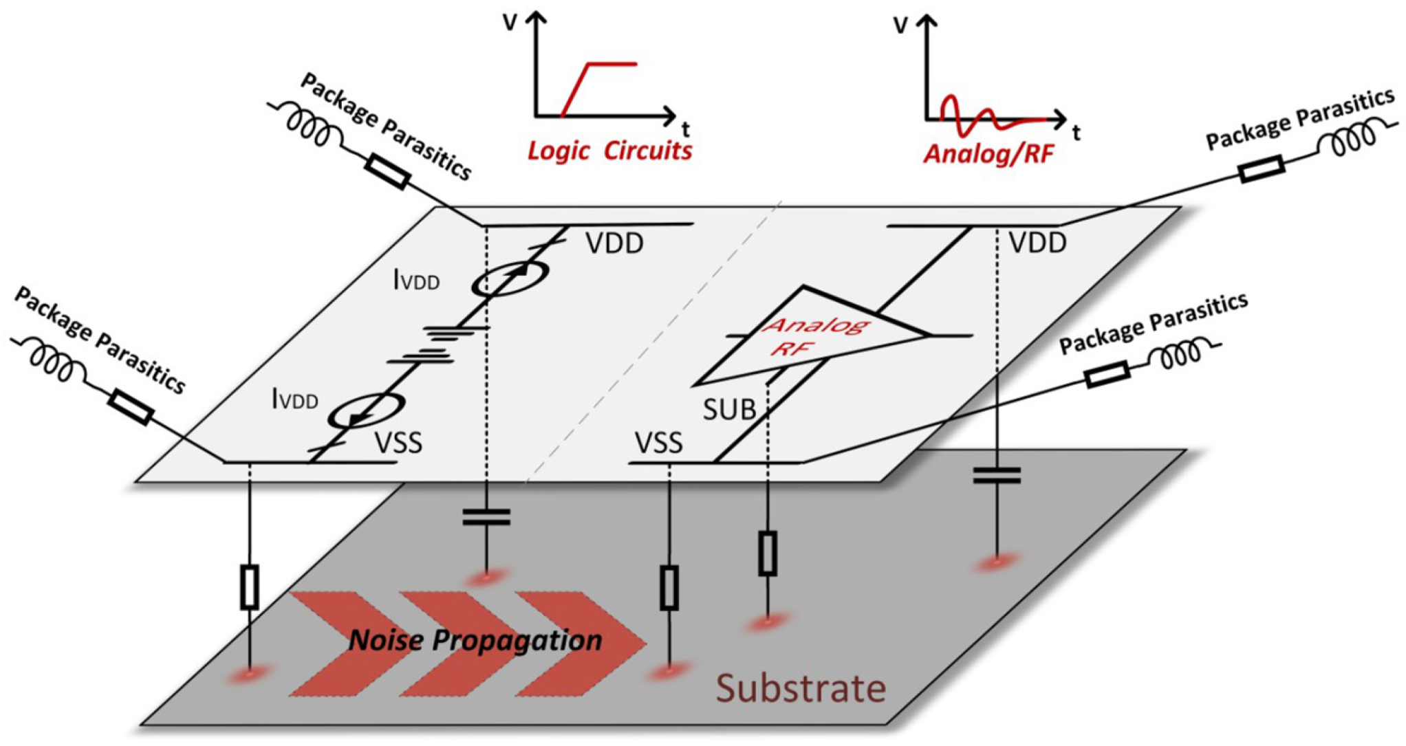
When digital devices make a state transition from one state to another, switching noise is injected into the substrate and propagates through the common substrate to the sensitive analog/RF circuits. The fast switching in digital blocks generates large current spikes across the power supply lines, causing noise generation in the parasitic inductances of the power supply interconnections of the integrated circuit (IC). The different areas of the silicon substrate are resistively/capacitively coupled to each other and since the substrate biasing contacts are tied to the ground, the supply noise is coupled directly to the substrate and interferes with the other blocks (
Figure 1). Substrate noise affects important performance specifications such as signal-to-noise ratio, gain and bandwidth [
2,
3,
4].
At the same time, newly arising technologies in automotive and mobile applications demand high performance and reliable designs. The increase in operating frequency and the extremely dense integration for minimizing the cost have caused the substrate coupling to become one of the most challenging design parameters. The complete radio spectrum usage of SoC, from 3 kHz to 30 GHz, and the wireless applications specifications with signal/power below background noise impose stringent constrains for the substrates effects. The problem gets even worse with the SoCs shift to millimeter wave ICs design and the enablement of 5G mobile communication SoC products.
Significant effort has been made to model and efficiently analyze the substrate noise coupling, but none of the proposed works have addressed the problem adequately. Most of the proposed noise simulation processes do not include the noise performance in each design level but focus on particular noise injection mechanism [
5,
6,
7]. A full SoC level noise approach is proposed by Badaroglu et al. [
8], Nagata [
9], and Noulis et al. [
10]. However, the first two proposed methodologies cannot be integrated in the current industry design flow and the latter is focused on crosstalk capturing through on-the-fly measurements and not simulations. Among the related methodologies, only in [
11,
12] is an analysis flow for the substrate noise estimation proposed from the silicon level to the package and PCB level (albeit limited versus its capacity to simulate all effects and the accuracy constraints).
In this paper, a novel substrate coupling modeling and analysis flow is presented in detail. Furthermore, a thoroughly analysis of the substrate noise sources and injections mechanisms is presented. The simulation crosstalk flow is fully compatible with the industry product level analog/RF and mixed signal design flow. This crosstalk noise simulation methodology includes the noise signals propagating through the substrate, the interconnect parasitics, and the package. Thus, it provides an overall estimation of the substrate noise effect on the circuit performance. A GHz region CMOS circuit de-gradated performance wise by kGate level digital logic acting as noise aggressor is used as a crosstalk vehicle for the validation of the proposed simulation flow. The crosstalk aware system on chip vehicle is designed in an RFCMOS 65 nm low power process. This technology process offers a dual gate dual gate oxide, 1.2 V core voltage, six metal layers, and temperature range from −40 °C to 125 °C [
13].
2. Substrate Noise Generation
In this section, the sources of the substrate noise are analyzed. The simultaneous operation of the digital block and the sensitive analog/RF circuits on the same die introduce two primary types of switching noise: power/ground noise and interconnect noise.
2.1. Simultaneous Switching Noise
The parasitic impedance in the power supply interconnects between on-chip and off-chip plays a major role in ICs performance. These parasitics come from printed circuit board (PCB) traces and package parasitics (i.e., bond wires). The simultaneous switching of the digital block operating at high frequency requires a significant amount of current, drawn from the power supply and therefore large current spikes are generated. This current spikes flow through the parasitic impedance of the power distribution network, causing voltage drops on the power supply voltage. Similarly, the current flowing from the digital block to the reference ground of the power supply causes voltage fluctuations. The voltage drop is given by
where
Leff and
Reff are the parasitic inductance and resistance of the power supply path. The first term is proportional to the rate of change in current and the second term referred as IR drop, is proportional to the magnitude of the current. The large values of the
dI/
dt dictates the inductance to be the dominant part of the impedance. When a current spike occurs, a voltage fluctuation is initiated and can be described by
where
θ and
k depend on the values of
R,
L, and
C parasitics and ζ is the damping factor determined by
From Equation (3) one can derive that for smaller L and larger R, the voltage fluctuation becomes faster. The crosstalk noise is generated by the capacitive and/or inductive coupling of a victim node and a switching aggressor node. Usually, the susceptibility to noise node is located in the sensitive analog/RF circuit.
2.2. Injection of Digital Switching Noise
In both analog/RF and digital circuitry blocks, the silicon substrate is biased via substrate contacts. The body of the NMOS transistor is the substrate surrounding the transistor channel. Hence, the biasing contacts of the NMOS transistors are directly connected to the substrate. In a digital circuit, for each gate there is at least one substrate contact. The large number of substrates contacts lowers the impedance of the substrate region of the digital circuit [
14]. Hence, all digital ground noise and ringing will also be present on the substrate. In the analog circuit, the substrate contacts are connected directly to the analog ground. Due to the substrate low impedance to the analog ground, the substrate noise in the analog region couples to the analog ground.
Another noise injection originates by the pn-junctions in NMOS transistors. The different doping regions of a transistor form parasitic diodes that normally are reverse biased. Both the drain and source are capacitively coupled to the body of the transistor. The parasitic capacitance of the reverse biased diode is given by
where
A is the area of the pn-junction,
q is the elementary charge,
εsi is the permittivity of the silicon,
NA and
ND are the respective doping levels of the p region and the n region,
Vbi is the built in voltage,
VD is the voltage across the diode. From Equation (4) it is derived that the parasitic capacitance is nonlinear and voltage dependent. At the PMOS transistor, the body is an n-well region. The source and the drain are resistively coupled to the n-well, while the n-well is capacitively coupled to the substrate through the pn-junction formed by the n-well and the substrate.
The body effect in MOS devices makes them especially susceptible to substrate noise reception. The drain current is mainly controlled by the gate-source voltage (
VGS) and in saturation region, it is affected by the threshold voltage (
Vtn) following the equation:
where
The threshold voltage depends on the voltage difference between source and bulk,
VSB. Hence, a voltage fluctuation on the body has a direct effect on the drain current. The body effect degrades the circuit performance mainly at low frequency [
15,
16].
Substrate noise is also received in the analog circuits via capacitive coupling to the substrate by interconnects. Noise coupling occurs both at the circuit and package level due to the on chip interconnects and power/ground pads. The coupling depends on the position of the interconnects and both the wire length and width. The wires capacitance has a high-pass filtering effect and therefore targets only the high frequency noise component. The highest capacitance coupling occurs between the lowest routing metal layer and the substrate. The capacitance gradually diminishes for upper metal layers. The capacitive coupling can act as an injection noise mechanism but can also receive substrate noise. Direct coupling between the analog and digital areas is avoided by placing them in different regions on the silicon die, but the common substrate allows the noise propagation from the noise aggressor to the victim.
Another source of substrate noise is impact ionization. The electrical field in the channel of the MOSFET becomes stronger as the power supply voltage is scaled less than the channel length. The strong electrical field accelerates the carriers and provides them with high kinetic energy. The hot carriers collides with atoms, promoting other electrons from the valence band into the conduction band. As a result, a current flows out from the body of the transistor and a voltage spike is generated. The impact ionization effect is included in standard transistor models [
17] and consequentially to the circuit simulations.
2.3. Substrate, PCB and Package Models
A reliable crosstalk analysis requires a reliable substrate model and inclusion of package and PCB properties as well. The principal components of the overall model should be the well impedance, the impedance between the origin of the noise generation and the substrate point of interest, the parasitic inductance induced by the connection of the substrate bias to analog ground, and the parasitic impedance of the package and printed circuit board.
For low frequencies, the substrate is mainly resistive while for high frequencies the dielectric behavior of the substrate plays a major role. Thus, the substrate model should include also the capacitive coupling for high frequencies. The substrate is purely resistive for frequencies up to
where
ps and
εsi are the resistivity and the permittivity of the substrate, respectively.
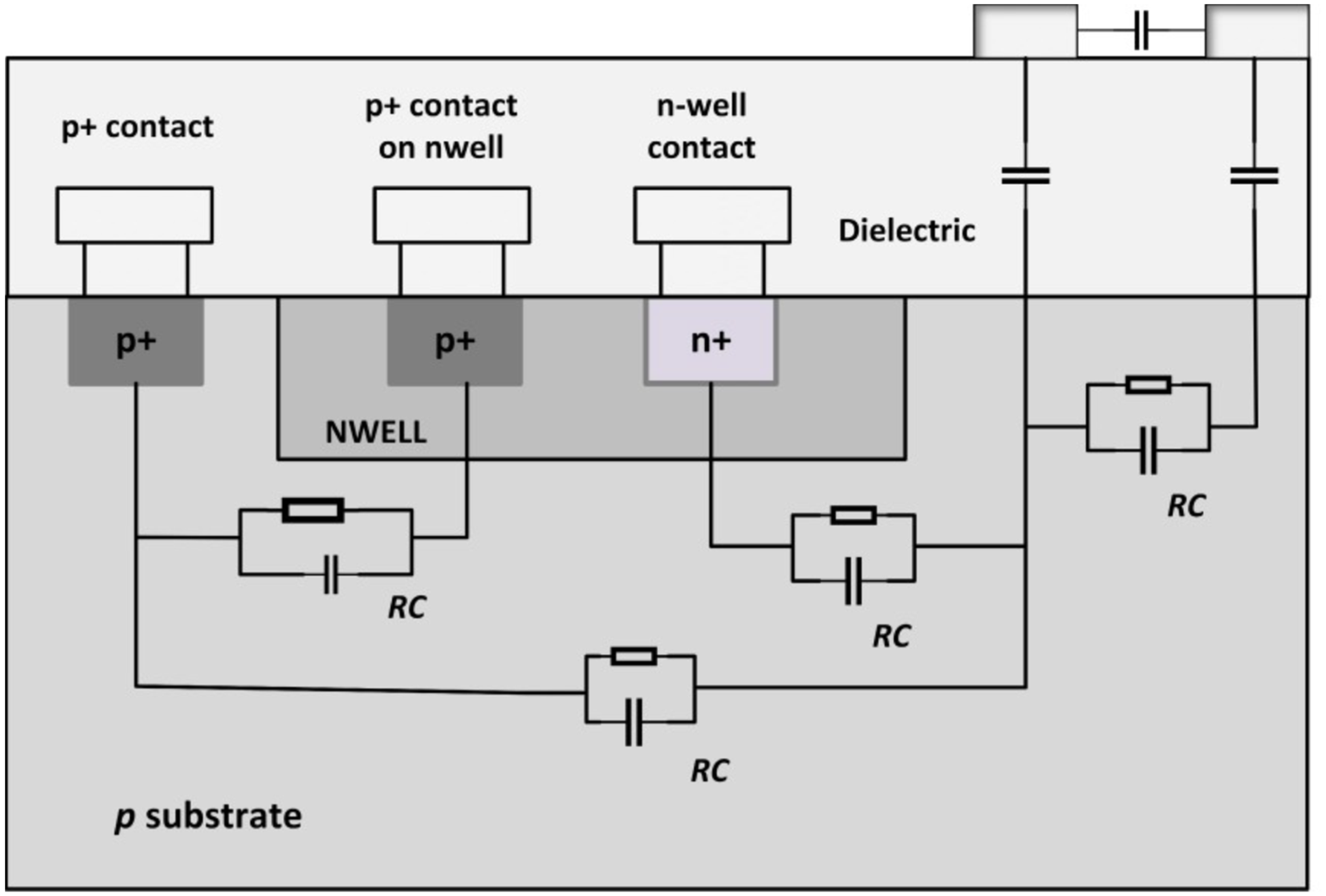
The critical process parameters are the bulk sensitivity, the bulk thickness, the well area junction capacitance, and the well-periphery junction capacitance. The technology files contains the substrate properties and the geometry data files indicates the substrate effective objects. A cross-section of the substrate model is indicatively shown in
Figure 2.
The model includes the substrate tap, the n well, the active area, interconnects with the substrate, and metal interconnects. The resistive and capacitive characteristics of the substrate are calculated by extracting the value of a resistor parallel to a capacitance following by [
18]
where
εsi is the relative permittivity of the silicon substrate,
ε0 is the absolute permittivity, and
p is the electrical resistivity.
The silicon substrate model for the proposed noise aware flow is extracted with a 2.5D Method of Moments (MOM) electromagnetic simulator. The substrate includes geometries with different doping and cannot be represented by a uniform equation. In the Method of Moments, the circuit geometry is divided into cells that have constant permittivity and resistivity. Discretizing the substrate results in a mesh of elements and the 2.5D EM (electromagnetic) simulator determines the current flow by considering each cell as a transmission line. For each element, the capacitance and resistance are derived to every other element as well. When all of the values are determined, the simulator computes the Green’s function for the current impulse at all points in space across all substrate boundaries and an S-parameters network is derived. Simulators such as 2.5D (but also 3D0 are available in the electronic design automation (EDA) market [
19].
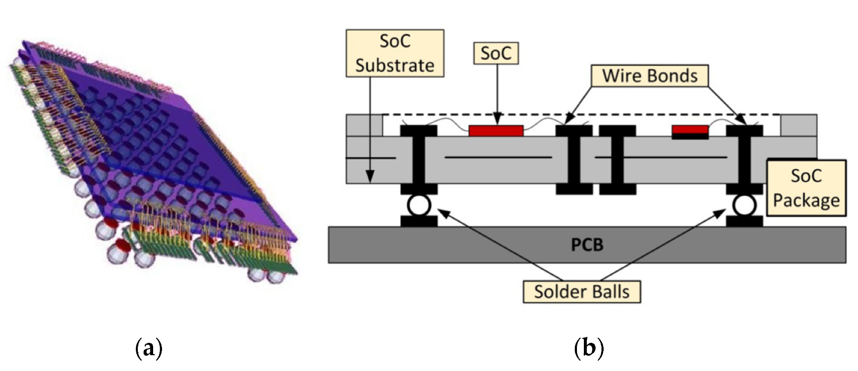
The package and PCB models of a SoC based component (
Figure 3) can be generated based on a MoM (Method of Moments) electromagnetic simulation. In order to optimize the simulation time, different models with different numbers of cells can be configured. Furthermore, the models can be developed as quadrupoles that constitute the signal path at the package and the PCB. The output results represent the inputs for electronic circuit simulators (i.e., Spice) and can be further analyzed.
The Spice models of the wire bonds, solder balls, vias, and PCB traces can be obtained by MoM analysis (
Figure 4). The wire bond is a gold non-symmetrical element (
Figure 4a) and its crucial parameters are the diameter and length. The SoC and package pads can be represented as squares. The series resistance and the shunt resistance of the wire bond can be neglected as it is a “short” element.
A representative solder ball structure with short interconnection lines is depicted in
Figure 4b. The configuration consists of two symmetrical balls on a PCB, a connecting trace on the bottom side of the BGA package, and a part of the BGA. The solder ball is a 3D element and hence another simulation tool based on the FDTD (finite difference time domain) method can be used for better modeling and simulation of the 3D object.
The input parameters are the diameter, spacing between balls, width of the copper traces, and connecting bridge between the balls, length of copper traces, and substrate thickness. The LC equivalent circuit of the solder balls is obtained by the simulator and it is based on it’s symmetrical structure. After the extraction of the LC parameters for the whole configuration, the L and C values for one solder ball are obtained (dividing by two the generated values based on the symmetry).
The via represents a discontinuity which cause a step change in the characteristic impedance of the signal path (
Figure 4c). For analyzing this type of element, the first step is to compare the hole diameter of via (“d”) and the length of via (“h”). If h >> d, via can be approximated with a conductive barrel placed between the two interconnected layers and the discontinuity act as two corners. If h ≈ d or h < d, the approximation from above is no longer valid and the influence of via barrel, respectively via capture pads must be taken into account using the electromagnetic simulator. Via is also a “short” element thus the lossless model does not include the series and shunt resistances.
3. Substrate Crosstalk Simulation Methodology
A substrate modeling approach was developed and a simulation analysis flow was followed. The block diagram of the proposed design flow is depicted in
Figure 5. This method enables the early-on simulation based substrate crosstalk impact capturing and does not require any additional on-chip circuitry to capture the substrate noise characteristics.
The proposed substrate noise analysis takes into account all of the design parameters of the SoC, from the block/circuit level to package and PCB. The overall simulation flow includes the electromagnetic (EM) model of the SoC common silicon substrate, the netlists and models of the on-chip circuits (analog/digital block), the package, the PCB, and the power supply rails. The analog block which is used as a test noise victim is a 5 GHz LNA, while the noise generator is a 90 kGates digital logic.
For the full chip simulation, a printed circuit model (PCB) model is extracted from a 2.5D electromagnetic simulator based on the Method of Moments (MOM). The model parameters were the insulator thickness −100 μm, copper thickness −35 μm, signal line length −5000 μm and width −1000μm. For the overall SoC substrate crosstalk modeling, a ball grid array (BGA) package model also is needed. The BGA package model is extracted from an electromagnetic simulator based on parameters of insulator thickness 8 μm, copper thickness 8 μm, signal line length 500 μm and width 250 μm.The digital noise aggressor consists of 90 kGates digital logic and is designed in an RFCMOS 65 nm process.
The digital circuitry is a chain of inverters. Due to the digital logic extreme large netlist size and the time-consuming simulation time at the transistor level, a gate level simulator was implemented to extract the switching noise currents from the digital blocks.
This noise currents are used as a primary figure-of-merit to determine the significance of switching noise at the overall circuit performance. The digital logic block is composed of 40 families of gates and each gate family is connected to the digital VDD and VSS supply rails providing two switching currents IVSS and IVDD. The gate families are identical inverter chains distributed with a uniform way onto the power and ground grid. Thus, the switching currents of each gate family can be monitored and simulated separately and exported in .csv form. The physical design of the digital block connected with the package and PCB model is simulated at a post-layout level and the IVDD and Ivss piece wise current sources are exported. These currents are represented by a piecewise linear (PWL) functions and translated as PWL current sources hanged onto the respective gate family location onto the power and ground metal grid. In total 80 I_PWL noise currents were extracted based on the gate number and the size of logic sub blocks. The IVSS current model sources are driven to the digital VSS supply rail of the chip and couples resistively to substrate while the IVDD PWL current source is driven to the digital VDD supply and is coupled to substrate capacitively. The switching noise currents IVDD and IVSS injected through the digital VDD and digital VSS contacts to the substrate represent the required inputs for the substrate crosstalk simulation. This modeling methodology of the digital circuit behavior provides a relatively small netlist size for the digital core and minimizes drastically the simulation time. In addition, while the gate level simulation approach is not a really advanced one, any other gate level simulation approach can be integrated in the proposed noise integrity flow, as long as, the connectivity information of each gate family is available, in relation to the power grid coordinates. Furthermore, as to support dynamic large signal analysis, the compatible formats for the currents would be either PWL time domain models or any other model that can provide the dynamic response of the drawing currents onto the power rails.
In
Table 1, a netlist of the digital logic is provided in RC extracted form, in schematic level and with the proposed digital model. Furthermore, in the table all of the device elements and the total nodes are presented for each method. The small netlist size of the gate model is efficient as to enable an overall simulation flow, overcoming the impractical simulation time required by standard verification methodology.
The model for the silicon substrate was extracted with a 2.5D MOM electromagnetic simulator. The silicon RC impedance transfer function was represented by an S-parameter substrate model file (.sNp). The model is based on the footprint description file of the effective layout (.gdsII) and the stack file where all of the process layers are described. The substrate of the used process, is a standard silicon substrate with 275 μm thickness without the metallic ground plane, and the bulk has an average resistivity of 10 Ω.cm. In addition, different types of substrate can be also modelled, such as epitaxial substrates (where better purity concentration and different material growth can be implemented) and since the applied methodology allows the 2.5D electromagnetic simulation of any substrate (as long as the stack and the layers of the process is described accurately in the input technology description file).
An algorithm used to extract the substrate aware circuit model-related data processing flow is shown in
Figure 6. The input data are the circuit net list and the mask design of the digital and analog/RF blocks. The netlist is processed so as the substrate effective nodes to be defined. From the other input, the gds file is extracted and modified in order only the substrate effective layout to be derived. Specifically, the substrate contacts connecting metal layer segments to substrate layers are recognized and the lengthy metal segments are shorted to either p-type or n-type diffusion layers. A substrate effective “tap” is defined by a combination of layers in order to distinguish it from a segment with only metal characteristics. During the processing of the layout, a new polygon is created which has, as a layer, the effective tap area and, as the net, the device bulk node. At the center of the polygon an extra pin is created. The effective substrate interface area is defined by the active devices which are represented as black boxes with their necessary pins. This area defines a layout footprint that may be either p-substrate bulk or n-substrate bulk depending on the bulk node of the corresponding device. The substrate model is simplified by merging effective layout objects or multiple counted devices into a single substrate interface area and all of the bulk nodes end up to a single node. The extracted model includes both the real and imaginary part. Therefore, the model capture the crosstalk effects at a broad frequency band ranging and is a reliable model for validating the circuits’ performance.
The output of this methodology comes after merging of the effective substrate model and the sub-node aware circuit netlist. The merging netlists create an .oa unified netlist resulting in a substrate crosstalk aware simulation. After the extraction of the model in .sNp file format, it is imported via an Nport and implemented in the simulation test bench.
The sensitive analog/RF part should be connected also to the Nport to capture the substrate noise performance. For this reason, the transistor model files were modified and added an extra substrate effective node (sub) were added, turning the transistor into a five terminal device. The extra node was placed in the deep n-well as it is shown in
Figure 7a. Modifications were also made at the component description format (CDF) parameters of the RF NMOS devices of the process design kit and the RF NMOS SPECTRE model. Similarly, in the inductors an extra node is added as it is shown in
Figure 7b. A respective workaround was carried out for all of the inductors models.
The above-modified substrate hidden aware models, for the NMOSFET RF device and the inductors, should be implemented for all of the respective devices that couple to substrate, and especially for voltage-controlled oscillator cases, for the MOS-Capacitors, and for the ESD diodes (especially for the diodes, which are available almost in all of the integrated circuit designs). For protection purposes, the coupling path can create parasitic currents, and therefore these are really crucial. The respective hidden bulk node aware p type diode cross-section and its symbol is provided in
Figure 7c.
4. Substrate Crosstalk Flow Validation
The proposed flow is applied to a SoC case study as to validate the substrate noise simulation flow. A full chip level simulation is performed to estimate the performance degradation of the analog/RF block caused by the switching noise currents generated by the digital logic. The simulation process includes the substrate, the interconnect parasitics, package and PCB contributions to the substrate noise signal spectrum.
For the LNA crosstalk victim, a cascode common source topology was selected due to its high power gain, good noise performance and low power consumption. The schematic of the LNA is presented in
Figure 8. The LNA achieves a maximum gain of 15.4 dB and input matching −18.4 dB at 5 GHz operation frequency.
The LNA is connected to a 1 V supply voltage and the cascode transistors M1 and M2 are implemented with width 250 μm and length 50 nm. The bias current is provided to the circuit by a current mirror (Mbias, M1), R1 and R2. The width of the transistor Mbias is chosen much smaller than the width of M1 in order to minimize the power overhead of the bias circuity. The high value of the resistor R2 provides a very low noise current that can be ignored. The degenerating inductors Lg (3 nH) and Ls (186 pH) provide the resistive term in the input impedance of MOS transistor and ameliorates the input impedance matching. The inductor Ld (847 pH) is used for the output matching of the amplifier.
The digital block consists of 40 gate families and each gate separately includes 2200 CMOS logic standard cells. To minimize the complexity of the digital block, a chain of inverters were chosen for the digital circuit [
20]. The supply voltage is 1.2 V and the clock frequency 100 MHz. The layout schematic of the LNA with the digital logic is presented in
Figure 9. The layout effective areas of the LNA transistors and the 40 gate families of the digital block were merged and have created the total substrate effective layout that acts as input to the EM simulator. The effective tap points of the analog and digital blocks are depicted on the physical implementation.
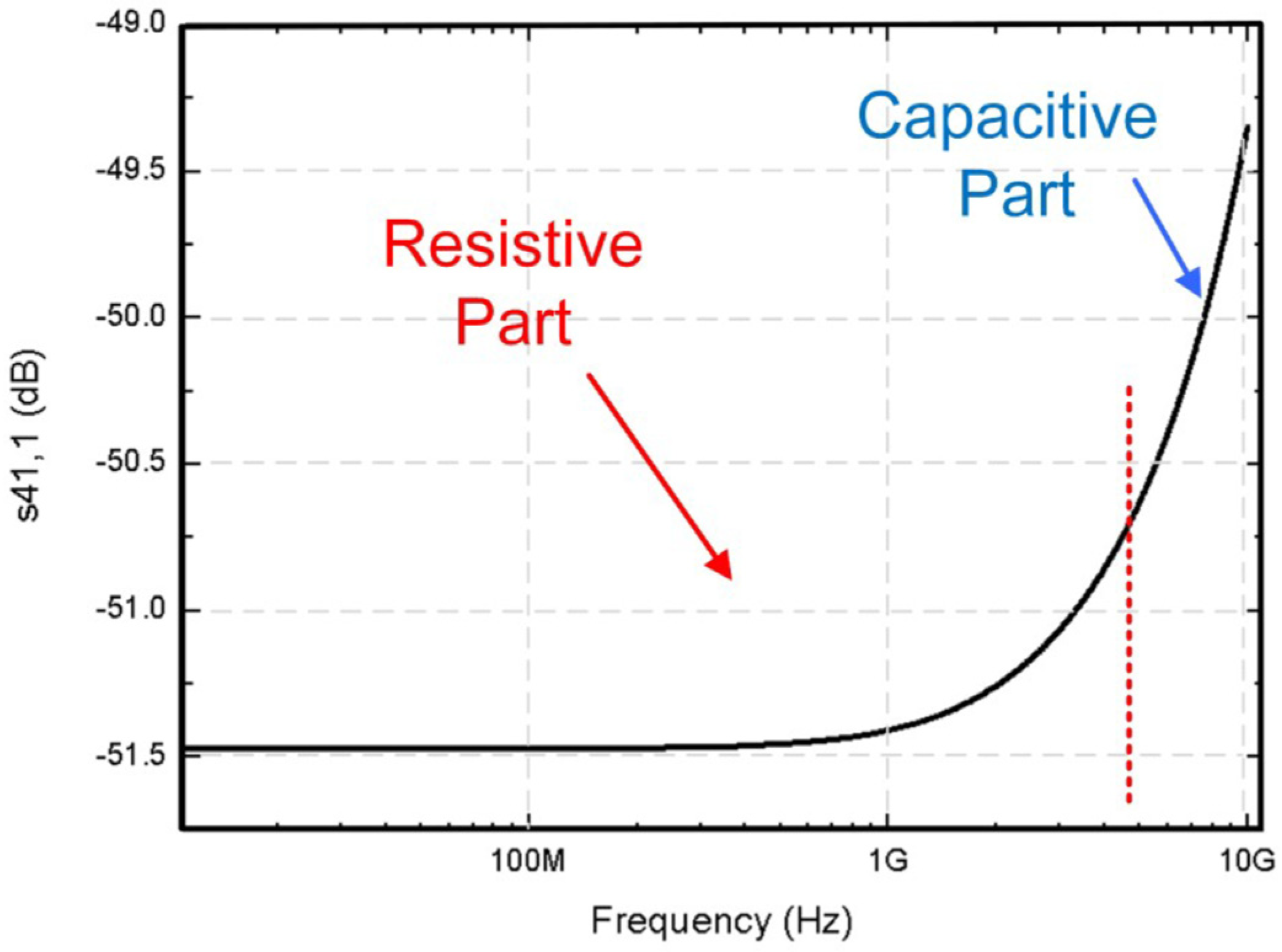
The resistive nature of the substrate is dominant in low frequencies, while the dielectric capacitive behavior in high frequencies. Thus, in the LNA design, only the RF NMOS devices come with substrate effective nodes as their operating frequency is in the low GHz frequency region. This behavior is clearly depicted in
Figure 10, where the substrate isolation (S-parameter) of the LNA effective substrate area to the gate family ‘1’ is provided. Until 2 to 5 GHz, the real part of the S41,1 is dominant, while the imaginary part dominates in higher frequencies.
The superiority of the proposed simulation flow is depicted in
Figure 11 where the standard simulation is compared to the proposed substrate crosstalk simulation flow. When the LNA is simulated with the standard flow, only the main spurs related to the harmonic frequencies of the circuit are captured together with a low noise floor, while the simulation with the proposed flow captures the substrate noise spurs related to the digital logic injected noise as well together with a way higher noise floor. By applying the proposed crosstalk analysis the degradation of the carrier voltage amplitude from −11.7 dBV to −19.9 dBV at 5G Hz is identified. This reduction is due to the package and PCB parasitics effects at the LNA impedance matching.
The proposed noise integrity simulation methodology, compared to the state-of-the art available methodologies [
7,
11,
14,
21] is the more efficient methodology available and is applicable from base band applications to RF and mmWave applications. In
Table 2 a comparison versus the state of the art is provided. First of all, it is the only methodology in the literature where additional substrate nodes are generated and attached to the compact models of the devices, enabling crosstalk simulation of the most important devices, such as the transistors and the inductors. This is the only way as to enable accurate cross-talk simulation of noise victims such as LNAs, VCOs (voltage control oscillators) and operational amplifiers, where the main device unit of the circuits are differential pairs with sources and bulks not connected to VSS but to local SOURCE terminal bias potentials. In the proposed methodology, the PDK models are on the fly updated, adding hidden substrate nodes, where the distributed substrate model will be attached. As a results the PDK (process design kit) models couple capacitively/resistively direct to substrate enabling identification of the most critical coupling paths. Furthermore, the proposed methodology includes all the parasitics, from the package (either this is a PGA (Pin grid array with bond-wires) or a BGA (flip chip with balls)) and the PCB, and forms a full system on chip simulation flow. This is not the case for [
21,
22]. In addition, in the proposed methodology, scattering parameters (s parameters) are used for the modeling of the passives, enabling way faster simulations times instead of using large RLC netlists. Among all of the other methodologies, an important benefit of this work is that the validity of this flow is not limited to low frequencies but from DC to mm Wave, since 3D EM models are generated and used, and PDK RF models are suitable adapted with substrate nodes. Therefore, the proposed methodology is valid from DC to mm Wave and from base band and power applications to RF, mobile communications, and radar. Finally, the respective simulation time is practical compared to other methodologies.
The simulation time is not provided as metric for comparison between the proposed work and the referenced state of the art. The main problem is that the simulation time depends on the available processing resources (CPUs, number of cores, memory used) and in every work these are not the same. Therefore, any comparison would not be an apple-to-apple comparison and would be misleading. Therefore, a comparison with “LOW” and “HIGH” simulation time flags, together with the description of each modeling methodology, was provided.
5. Conclusions
A novel analysis and straightforward substrate coupling simulation methodology was presented. The proposed methodology can be seamlessly integrated into the industry design flow for full SoC level chip simulations from baseband to high frequency SoC designs. For the first time, designers can have an insight from the early design phase to the product release phase into critical coupling paths and design parameters either these are related to the PCB, package, substrate and related power grid distributions or circuit architectures-digital and analog/RF– themselves. In terms of improvements, better accuracy can be achieved, especially in the higher frequency range, where the capacitive coupling between the n-well taps and the substrate should be concerned, adapting suitably all of the RF devices models and CDF parameters (such as the inductors and the capacitors).
Noise integrity simulation is also a main concern in through silicon vias (TSV) based 3D system on chip designs [
22,
23,
24,
25,
26]. TSVs are imposing new noise coupling paths into the substrate. As a result, a noise integrity simulation methodology for semiconductor materials types is required. The effects of the power supply and ground network inductance on noise victim performance is also crucial as to establish a solid methodology for simulating noise coupling. In future research, the methodology proposed in this work can be extended as to include 2D SoCs and 3D integrated circuits.


 ,
, 


