


Abstract
This work reports the results of a study on the optical, morphological, and structural properties of cesium lead bromide iodide mixed perovskite thin films (CsPbBr3−xIx), synthesized by sequential evaporation of precursors (CsBr, PbBr2, PbI2). First, the deposition conditions were optimized to obtain thin films predominantly composed of the pure CsPbBr3 phase. Subsequently, the influence of partial substitution of Br− by I− on the film properties was investigated. Particular emphasis was placed on evaluating the effect of partial Pb2+ substitution by Zn2+ on the optical, morphological, electronic, and structural properties using optical transmittance, photoluminescence, scanning electron microscopy (SEM), X-ray diffraction (XRD), Urbach energy analysis, and density functional theory (DFT) calculations. Zn2+-doped CsPbBr3−xIx films were prepared by evaporating a ZnBr2 layer onto the pre-deposited PbBr2/PbI2 precursor layers. It was found that Zn2+-doped inorganic CsPbBr3−xIx perovskite films exhibit enhanced crystallinity and improved surface morphology. Additionally, photoluminescence characterization confirms that non-radiative recombination decreases significantly, apparently due to a reduction in intrinsic defect density. The effect of Zn2+ doping on the power conversion efficiency of carbon-based planar solar cells was also evaluated. Collectively, Urbach energy, photoluminescence, and SEM analyses revealed that the optimal Zn2+ doping range for CsPbBr3−xIx perovskite films is ≤5%.
1. Introduction
Organic–inorganic hybrid perovskite solar cells have been intensively investigated since their discovery, owing to their outstanding optoelectronic properties, including high absorption coefficients, long carrier diffusion lengths, low trap density, and ease of synthesis via solution growth and thermal evaporation [1,2,3,4,5,6,7,8,9,10]. These attributes have enabled remarkable efficiency improvements over the past decade, with single-junction perovskite devices now surpassing 26% and silicon-perovskite tandems exceeding 34% [11,12,13,14,15]. Despite these advances, critical challenges to the long-term stability of these devices continue to limit their practical application and commercialization.
This instability stems primarily from the volatility of the organic cations typically used in traditional organic–inorganic hybrid PSCs, which leads to poor moisture and thermal stability [16,17,18], thereby limiting their market adoption. To prevent this degradation, inorganic cesium ions (Cs+) are used to replace the organic cations, allowing the manufacture of all-inorganic PSCs [19,20,21] with which conversion efficiencies exceeding 21% have been obtained [22]. Among all-inorganic PSCs, those based on CsPbI3, CsPbBr3−xIx, and CsPbBr3 have experienced greater development [23]. It is worth noting that among all the studied all-inorganic perovskites, devices based on CsPbI3 have achieved the highest PCE (over 21%). However, this exhibits severe degradation because the α-CsPbI3 phase can only be stable above 330 °C, leading to its rapid conversion to the non-photoactive phase (-CsPbI3) at room temperature [15,16]. On the contrary, CsPbBr3 is a stable phase. Still, it has a bandgap of 2.35 eV, which limits its light-harvesting capability in the visible region, resulting in low photocurrent and, therefore, low conversion efficiency [17,18,19]. On the other hand, mixed-halide inorganic perovskites (CsPbI3−xBrx) offer improved absorption capacity and structural stability when a suitable ratio of halide anions is used. In particular, mixed-halide perovskites with an amount of iodine less than or equal to the composition CsPbIBr2 (Eg = 2.05 eV) exhibit both better bandgap and phase stability, rendering them a good alternative for the fabrication of PSCs [22,23]. B-site doping with other metal ions has also been shown to be an effective method to improve the efficiency and stability of CsPbIBr2-based cells [24,25,26,27]. In particular, partial replacement of Pb2+ by Zn2+ has been successfully investigated in several inorganic perovskite materials [28,29,30,31].
In this study, special emphasis is placed on the influence that the partial substitution of the Pb2+ cation by Zn2+ has on the optical, morphological, structural, and electronic properties of cesium lead bromide iodide mixed perovskite thin films (CsPbBr3−xIx), synthesized by sequential evaporation of precursors (CsBr, PbBr2, PbI2). This work contributes to the study of inorganic CsPbBr3−xIx perovskite films by investigating the simultaneous incorporation of I and Zn through sequential evaporation. This reproducible and potentially scalable deposition route deserves further exploration.
Through XRD measurements, we have found that CsPbBr3 films present good phase stability under normal humidity and lighting conditions. However, the CsPbBr3−xIx films prepared with an amount of iodine greater than that corresponding to the composition CsPbBr2I exhibit severe degradation associated with a transition from the α-phase to the non-photoactive -phase at room temperature. To avoid degradation under normal humidity and lighting conditions, samples with the composition CsPbBr2.7I0.3 were prepared and exhibited good phase stability. These were characterized using XRD, SEM, photoluminescence, spectral transmittance, and Urbach energy measurements to evaluate the effect of Pb2+ substitution by Zn2+ on its optical, structural, morphological, and crystallographic properties. The influence of Zn2+ doping was also studied using DFT calculations. Therefore, the main contribution of this study lies in clarifying the composition–property relationships of Zn- and I-modified CsPbBr3 films prepared by sequential evaporation.
2. Materials and Methods
CsPbBr3−xIx thin films were prepared using a method consisting of the sequential evaporation of its precursors (PbBr2, PbI2, CsBr), deposited on a soda-lime glass substrate at room temperature from Knudsen cell crucibles at growth rates of around 5 Å/s. These are subsequently annealed under normal air conditions at temperatures ranging from 200 °C to 350 °C for 15 min. Good reproducibility of both the composition and properties of the evaluated samples was achieved using equipment with facilities to electronically control the evaporation temperature and deposition rate of precursors via Proportional–Integral–Derivative (PID) and Pulse Width Modulation (PWM) algorithms. Details of the equipment used to prepare the CsPbBr3−xIx films are described in a previously published paper (see Ref. [32]).
The chemical composition of the resulting compound was varied over a wide range by adjusting the thickness ratio of the precursors, which was determined using a thickness monitor. Initially, a 450 nm-thick layer of PbBr2 was deposited, followed by consecutive deposition of the PbI2 and CsBr layers. Through a study of parameters, conditions were found to produce CsPbBr3−xIx films, with compositions ranging from x = 0 (CsPbBr3) to x = 2 (CsPbBrI2). The influence that the partial substitution of Pb2+ for Zn2+ (obtained by additional evaporation of a layer of ZnBr2) produces on the optical, morphological, structural, and electronic properties of CsPbBr3−xIx films was also studied. This study was performed using reference perovskite films with a CsPbBr2.7I0.3 composition that exhibit good stability under humidity and ambient light.
The prepared samples were characterized by transmittance and reflectance measurements performed using a Varian–Cary 5000 spectrophotometer (Agilent Technologies, Inc., Santa Clara, CA, USA), as well as by XRD measurements performed with a Philips X’Pert Pro PANalytical diffractometer, using Cu Kα radiation (1.540598 Å), an acceleration voltage of 40 kV, and a current of 40 mA. The film thickness was determined using a Maxtec TM-400 (Maxtek, Inc., Salt Lake City, UT, USA) thickness monitor, calibrated with a Veeco Dektak 150 surface profiler (Veeco Instruments Inc., Tucson, AZ, USA). The morphological characterization was performed using an SEM (TESCAN Vega 3, TESCAN Brno, s.r.o., Brno, Czech Republic).
The stoichiometry of the films obtained by sequential evaporation was carefully controlled by monitoring the deposited thickness of each precursor using a quartz crystal microbalance (QCM, Maxtek). The amounts of CsBr and PbBr2 were calculated using their molar masses and densities to achieve a molar ratio close to 1:1, required for the formation of the CsPbBr3 perovskite phase. In particular, the masses of CsBr and PbBr2 used were nearly stoichiometric, minimizing the occurrence of cesium- or lead-rich conditions that could favor the formation of secondary phases, such as Cs4PbBr6 or residual PbBr2.
3. Results
3.1. Structural Properties Study
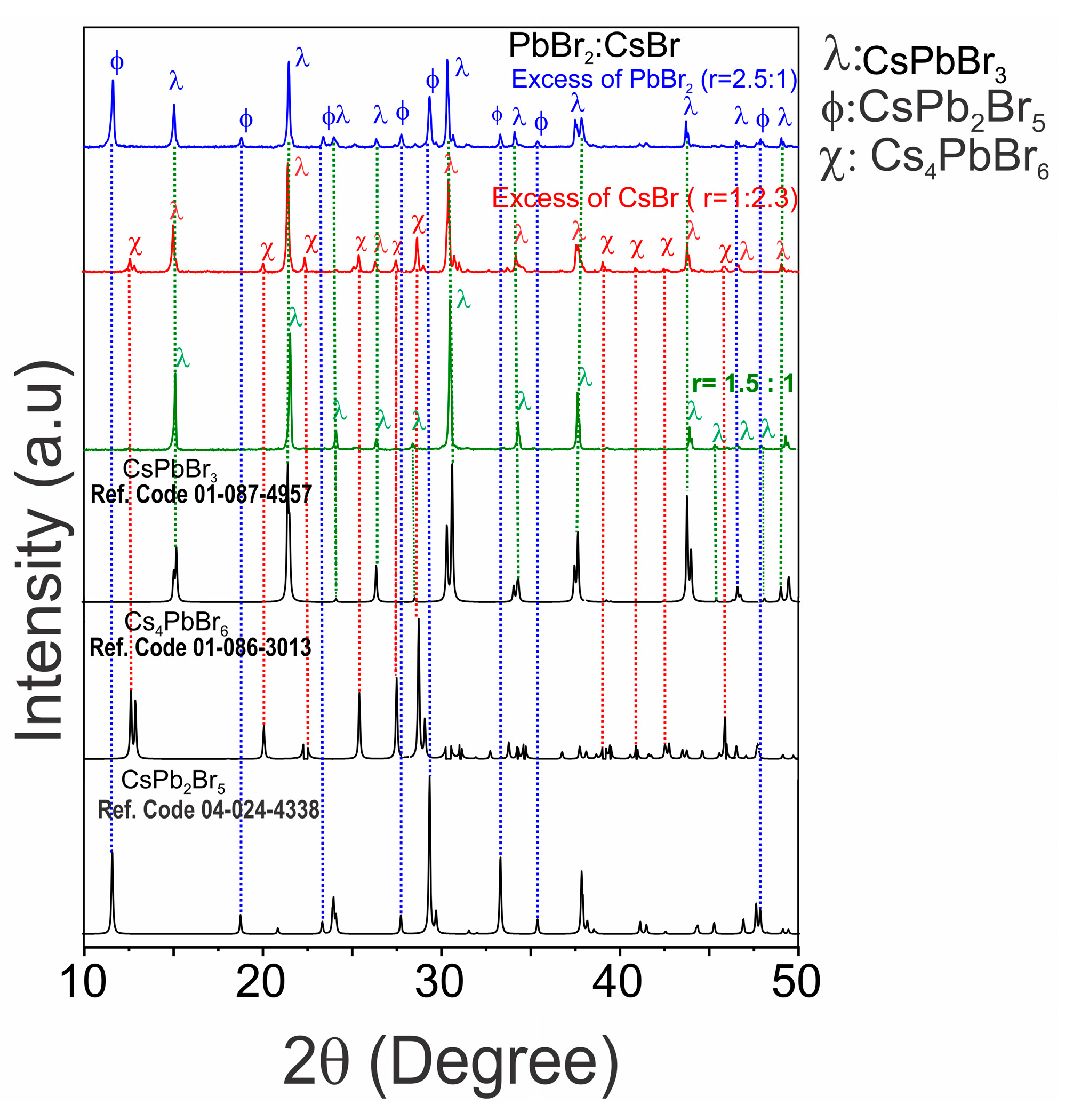
Initially, a study was conducted to identify synthesis conditions for growing thin films of CsPbBr3 composition free of secondary phases. For this, the ratio of PbBr2/CsBr thicknesses was varied between 1:2.3 and 2.5:1, and the annealing temperature after deposition was set to room temperature. The crystalline phase in which these samples grew was established through XRD measurements.
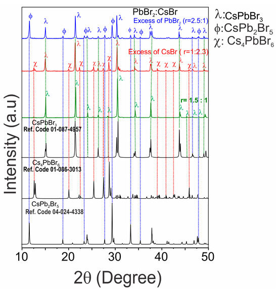
Figure 1 shows the XRD patterns of the cesium lead bromide films with different thickness ratios of the precursors. This study showed that the obtained samples consisted of a mixture of different phases, including cubic and orthorhombic CsPbBr3 phases, as well as secondary phases of other ternary compounds. The diffractograms shown in Figure 1 reveal that the films deposited using a thickness ratio r of 1.5:1 grow only in the orthorhombic CsPbBr3 phase (ICDD 01-087-4957), whereas films deposited with an excess of CsBr (r = 1:2:3 ratio) grow with a mixture of the orthorhombic CsPbBr3 phases and the secondary Cs4PbBr6 phase (ICDD01-086-3013). On the other hand, films deposited with an excess of PbBr2 (r = 2.5:1 ratio) result in samples that include a mixture of the orthorhombic CsPbBr3 and CsPb2Br5 phases (ICDC 04-024-4338). Other authors have reported similar results [33,34]. The following reactions can describe the formation of CsPb2Br5 and Cs4PbBr6 [35]:
CsBr + PbBr2 → CsPbBr3
CsPbBr3 + PbBr2 → CsPb2Br5
CsPbBr3 + 3CsBr → Cs4PbBr6
Figure 1.
X-ray diffraction patterns of perovskite thin films deposited at room temperature by sequential evaporation of their precursors (PbBr2/CsBr), varying the PbBr2/CsBr thickness ratio.
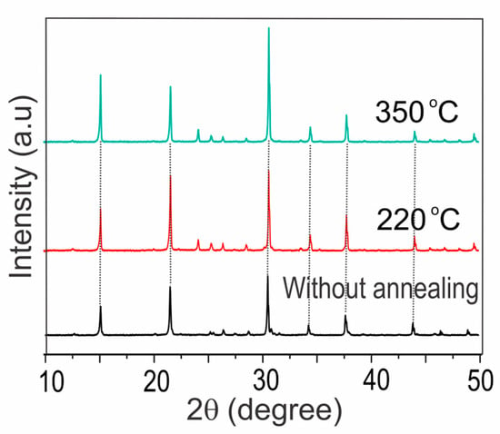
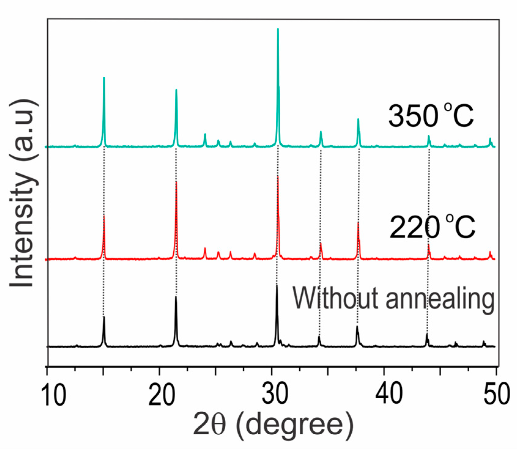
After deposition of perovskite films grown with a single-phase CsPbBr3, they were subjected to annealing in air at temperatures ranging between 220 °C and 350 °C, in an attempt to improve their properties. Figure 2 shows diffractograms of CsPbBr3 thin films annealed in air at temperatures ranging from room temperature (without annealing) to 350 °C, for 15 min. The XRD pattern displayed in Figure 2 reveals that the post-thermal treatment does not affect the crystalline structure of the perovskite films. However, increasing the annealing temperature increases the intensity of the reflections, apparently associated with an improved degree of ordering of the crystallographic planes.
Figure 2.
XRD patterns of CsPbBr3 thin films annealed at different temperatures in air.
Once secondary-phase-free CsPbBr3 thin films were obtained, a study was carried out to prepare CsPbBr3−xIx thin films by partially replacing the Br− anion with iodine in CsPbBr3 films, following the methodology described above.
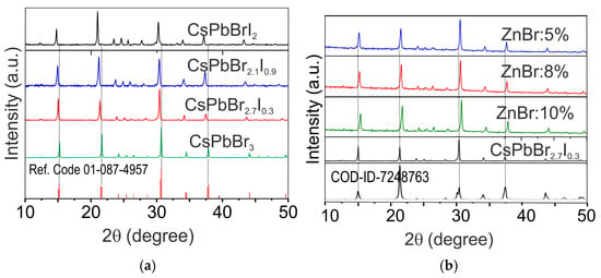
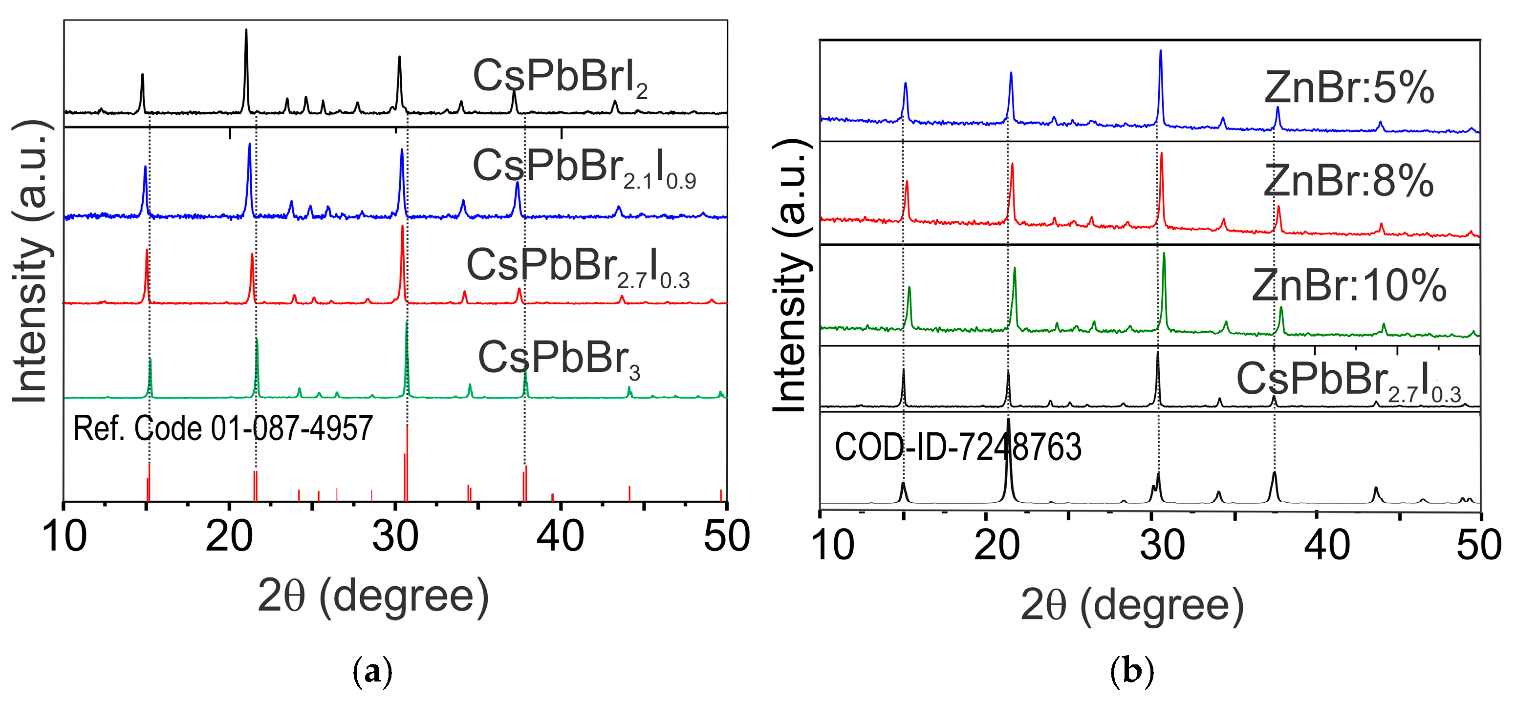
In Figure 3a, the XRD patterns of CsPbBr3−xIx films prepared by varying the molar ratio x between x = 0 and x = 2 are displayed. These results reveal that CSPbBr3 (x = 0) films exhibit only reflections corresponding to the orthorhombic phase of CsPbBr3, and when the iodine content increases in the CsPbBr3−xIx sample, the crystalline structure does not change. However, the reflections observed in the XRD pattern shift towards lower 2θ values as the iodine concentration increases. This is an expected behavior, taking into account that iodine has an ionic radius greater than that of bromine, which leads to an expansion of the CsPbBr3−xIx crystal lattice when the Br− anion is replaced by I−. This expansion of the lattice leads to an increase in the lattice constant, which is manifested in a displacement of diffraction peaks.
Figure 3.
(a) XRD patterns of CsPbBr3−xIx films, prepared by varying the molar ratio x between x = 0 and x = 2. (b) XRD pattern of CsPbBr2.7I0.3 films doped with Zn2+ at atomic percentages ranging from 0% to 10%.
Figure 3b compares the XRD spectrum of the reference CsPbBr2.7I0.3 sample with those in which Zn2+ replaces the cation Pb2+ in an atomic percentage that varied between 0% and 10%. These results reveal that CsPbBr2.7I0.3 exhibits only reflections corresponding to the orthorombic phase, and when Zn2+ ions substitute the Pb2+ cation, the crystalline structure does not change. However, the reflections observed in the XRD pattern shift towards larger 2θ values when the percentage of substitution of Pb2+ by Zn2+ increases. This shift is because the ionic radius of Zn2+ is smaller than that of Pb2+, which causes a reduction in the size of the unit cell, and according to Bragg’s law (nλ = 2d sinθ), for the relationship to be preserved, the angle θ must increase.
In this growth methodology, the precursors are initially deposited as independent layers, and subsequent heat treatment is therefore necessary to promote interdiffusion among the constituents and to favor the solid-state reaction that forms the perovskite phase. Temperatures above 130 °C were found to facilitate precursor diffusion, improve film crystallinity, and promote complete reaction between the different deposited species, particularly in the mixed-halide (Br/I) and Zn-incorporated compositions studied in this work.
Regarding the observed crystalline phase, it should be noted that CsPbBr3 transitions to a cubic phase at elevated temperatures during heating. However, X-ray diffraction analyses were performed after the samples had cooled to room temperature. Under these conditions, CsPbBr3 typically undergoes a return transition to the orthorhombic phase, which is the thermodynamically stable phase at room temperature. Therefore, although the films were annealed at temperatures above 130 °C, the observation of an orthorhombic structure in the XRD patterns is consistent with the expected behavior for this type of material after cooling. Additionally, the incorporation of iodine and zinc may slightly modify the lattice parameters, structural distortion, and phase-transition temperature, thereby stabilizing the orthorhombic structure observed at room temperature.
3.2. Optical Properties Study
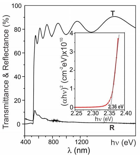
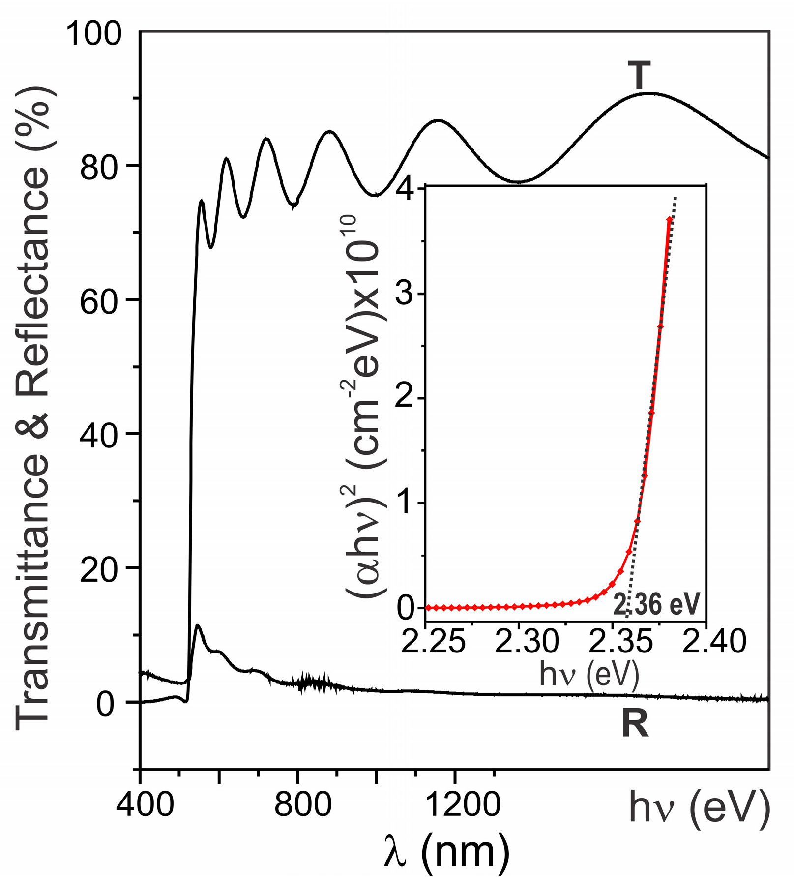
Typical transmittance, reflectance, and curves of CsPbBr3 thin films deposited under optimal conditions are displayed in Figure 4. The absorption coefficient α was determined from the transmittance T and reflectance R curves, using the following relationship [36].
Figure 4.
Transmittance, reflectance, and curves of a typical CsPbBr3 thin film deposited by sequential evaporation.
The value of the energy gap Eg is obtained from the intercept with the axis of the curve of (tauc curve).
The transmittance curves were found to have a steep slope near the cut-off wavelength (the edge of the conduction band), indicating that, in these samples, photon absorption occurs predominantly through fundamental absorption, which induces band-to-band carrier transitions. From this behavior, it can be concluded that the CsPbBr3 films deposited by sequential evaporation exhibit a low density of states arising from native defects. On the other hand, the annealing temperature did not affect the energy gap of the CsPbBr3 films. However, the thermal post-treatment slightly affects the transmittance intensity, apparently due to increased roughness induced by increased grain size.
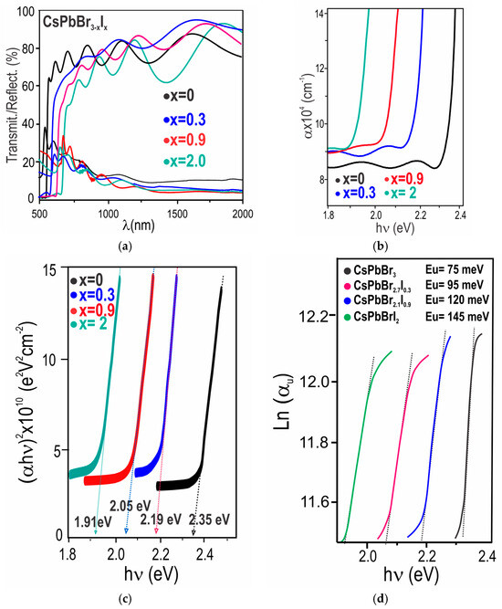
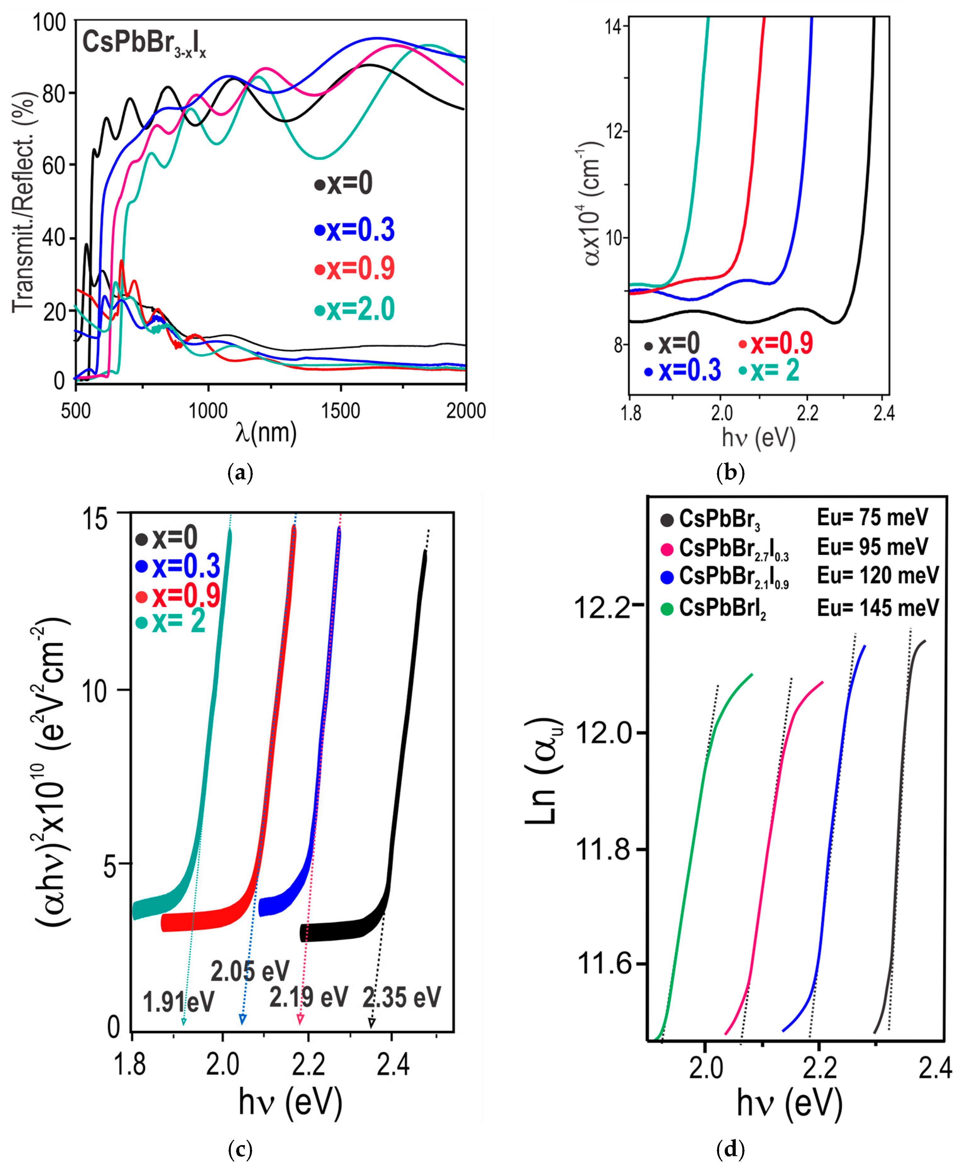
The influence of the molar ratio x on the optical properties of CsPbBr3−xIx films was also studied by spectral transmittance and reflectance measurements. Typical transmittance and reflectance spectra of CsPbBr3−xIx are shown in Figure 5a. Moreover, the α vs. hν and (αhν)2 vs. hν curves (Tauc curves) are shown in Figure 5b and Figure 5c, respectively. By plotting ln(α) vs. hν, the Urbach energy value can be determined from the slope of the curves. Figure 5d shows ln(α) vs. hν curves (near the band edge) for samples prepared with different molar ratios x, indicating the EU value calculated from their respective slopes.
Figure 5.
(a) Transmittance and reflectance spectra of CsPbBr3−xIx thin films prepared with different molar ratios x. (b) α vs. hν curves. (c) (αhν)2 vs. hν curves, corresponding to the Tauc plots used to estimate the optical band gap, as indicated by the dotted lines. (d) Near-band-edge ln(α) vs. hν curves used to determine the Urbach energy EU for CsPbBr3−xIx films with different molar ratios x. The optical band gap is indicated by the dotted lines.
It is observed from the Tauc plots in Figure 5c. that the energy gap Eg of CsPbBr3−xIx films decreases from 2.35 eV to 1.91 eV when iodine substitution increases its molar concentration from x = 0 to x = 2. Smaller band gap values are advantageous for fabricating solar cells with higher efficiency. However, when Br is excessively substituted by I, the perovskite films rapidly degrade into a non-photosensitive phase.
It is also observed in Figure 5a that the slope of the transmittance curves decreases with increasing substitution of Br by iodine in CsPbBr3−xIx films. This behavior is associated with the formation of structural defects that lead to band distortion, generating state tails that extend the bands within the band gap, inducing a decrease in the slope of the transmittance curves. Therefore, the absorption via transitions between band tail states indicates how much structural disorder (stress and dislocation) can influence the optical properties. The absorption coefficient near the band edge (αU), which is mainly influenced by absorption in band tail states, can be determined using the Urbach relation (Equation (5)) [37].
where Ei and αO are constants and EU is the Urbach energy.
Considering that the Urbach energy is related to the density of states located in the band gap induced by structural disorder, the results in Figure 5d reveal that increasing iodine concentration leads to an increase in the Urbach energy, indicating that an increase in the density of structural defects is induced by the incorporation of iodine into the perovskite structure, apparently because the ionic radius of iodine (2.2 Å) is larger than that of bromine (1.96 Å) [38].
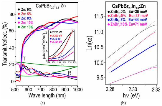
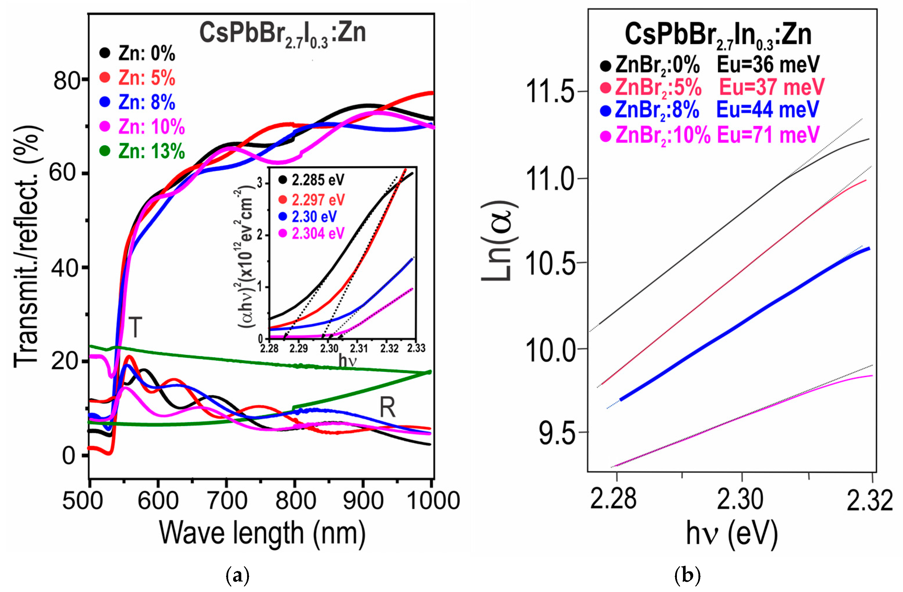
The influence of partial substitution of the Pb2+ cation by Zn2+ ions on the optical properties of a sample with the composition CsPbBr3−xIx was also studied. Figure 6a shows typical transmittance and reflectance spectra and the corresponding Tauc curves for a reference film with composition CsPbBr2.7I0.3 in which Pb2+ was substituted by Zn2+ at atomic percentages ranging from 0% to 13%. Figure 6b presents the corresponding ln(α) vs. hν curves near the band edge, used for estimating the Urbach energy.
Figure 6.
(a) Curves of transmittance and reflectance corresponding to a reference sample with composition CsPbBr2.7I0.3, to which the Pb2+ cation was replaced by Zn2+ in different atomic percentages. The inset shows the corresponding Tauc plots, with the optical band gap indicated by the dotted lines. (b) Curves of ln(α) vs. hν showing the Eu values obtained for a reference sample with composition CsPbBr2.7I0.3, doped with Zn2+ in different atomic percentages. The Eu values shown at the top of the graph were obtained from the slope of the dotted linear fits.
The results in Figure 6a show that replacing Pb2+ with Zn2+ at low concentrations has little effect on the energy gap of the studied sample, indicating that, under these conditions, the band structure is slightly affected. However, when the substitution of Pb2+ with Zn2+ is high (greater than 10%), the transmittance decreases strongly. No maximum and minimum are observed due to interference effects, indicating that these types of samples have a high degree of crystalline disorder, which gives rise to a high dispersion of incident radiation that destroys the coherence of the rays that overlap to generate constructive interference. On the other hand, it is observed that the slope of the transmittance curves of the samples with low Pb2+ substitutions by Zn2+ (≤5%) is slightly affected. However, when the Pb2+ replacement percentage exceeds 6%, the slope decreases more sharply. This behavior can be explained by considering that the replacement of Pb2+ by Zn2+ generates structural defects because the ionic radius of the Pb2+ (1.2 Å) is much larger than that of Zn2+ (0.74 Å). This situation generates band states within the gap, causing a decrease in the slope of the transmittance curves.
Figure 6b displays curves of ln(α) vs. hν (near the edge of the band) of a sample with composition CsPbBr2.7I0.3 to which Zn2+ replaced the cation Pb2+ in an atomic percentage that varied between 0% and 10%. The Eu value calculated from the slope of the ln (α) vs. hν curves proved to be less than 44 meV for samples in which Pb2+ was replaced by Zn2+ at a percentage ≤ 8%, indicating that they exhibit good crystalline quality. On the contrary, when a Pb2+ replacement is made with a percentage of Zn2+ ≥ 8%, the Eu value increases significantly, indicating that, in this case, there is high structural disorder.
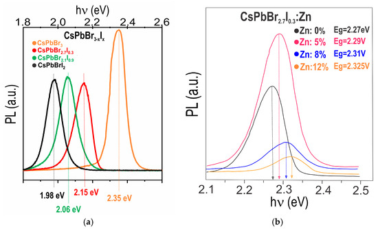
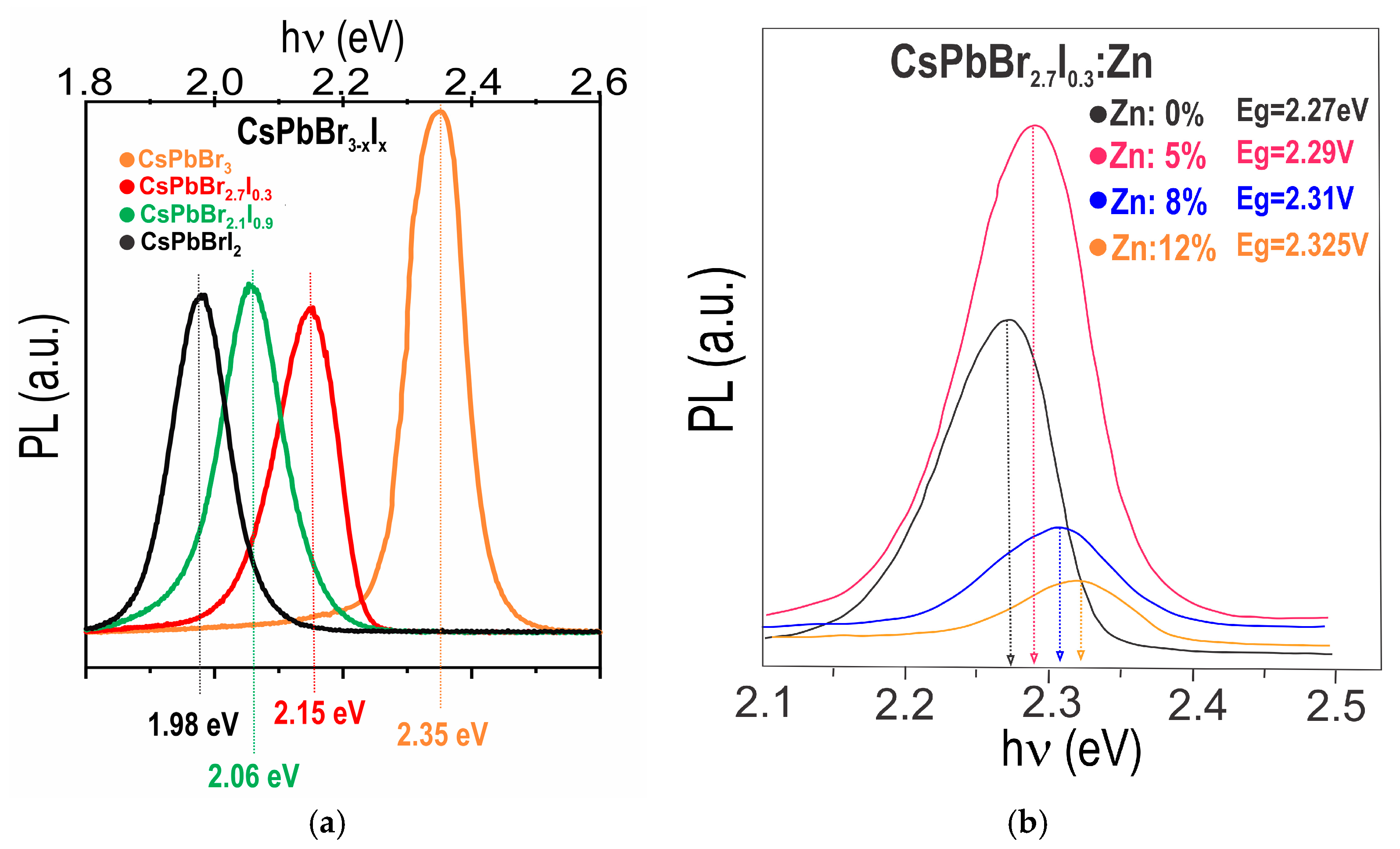
The influence of both the molar ratio x and the partial substitution of the Pb2+ cation by Zn2+ on the photoluminescence (PL) emitted by CsPbBr3−xIx thin films excited with a 400 nm laser was also evaluated in this study. In Figure 7, PL spectra of CsPbBr3−xIx thin films prepared with different molar ratios x and doped with Zn at different atomic percentages are displayed.
Figure 7.
Photoluminescence spectra of: (a) CsPbBr3−xIx thin films, prepared with different molar ratios x, and (b) a reference sample with composition CsPbBr2.7I0.3, doped with Zn in atomic percentages, varying between 0 and 12%. The optical band gap is indicated by the dotted lines in both graphics.
The results of Figure 7a show that an increase in the substitution of Br by iodine induces a reduction in the energy gap Eg from 2.35 eV (x = 0) to 1.98 eV (x = 2), in agreement with results reported by other authors [39,40] and with those previously obtained from Tauc curves. On the other hand, the PL spectra are symmetric, indicating that the radiative emission is primarily due to fundamental transitions between the valence and conduction bands. It is also observed that the CsPbBr3 sample exhibits a PL intensity that is significantly higher than that of the other CsPbBr3−xIx samples. This behavior could be explained by assuming that substituting iodine for Br in the CsPbBr3 film generates non-radiative recombination centers associated with deep emission levels. Poor crystalline ordering in this type of sample could also contribute to the reduction in PL intensity.
It can also be observed in Figure 7b that the PL spectra of films prepared by substituting Pb2+ with Zn2+ at Zn2+ concentrations below 6% are quite symmetrical. Still, this symmetry is lost when Zn2+ substitution exceeds 6% by atomic percentage. This behavior could be explained by assuming that the emission produced by samples prepared by substituting Pb2+ for Zn2+ at concentrations below 6% is primarily due to fundamental transitions between states in the conduction and valence bands. In comparison, films prepared with higher Zn2+ percentages emit, in addition to fundamental radiation, radiation induced by transitions involving energy levels within the band gap. These additional emission features may be associated with native defects, impurities, local compositional fluctuations, partial halide segregation, or slightly different compositional domains with distinct band gap energies. Although no clear secondary crystalline phases were detected by XRD, the presence of local compositional heterogeneities cannot be completely ruled out.
It is also observed that CsPbBr2.7I0.3 films prepared by substituting Pb2+ with high atomic percentages of Zn2+ exhibit PL spectra with very low intensity. This behavior could be explained by poor crystalline quality and by the generation of non-radiative recombination centers associated with deep emission levels, induced by the excess substitution of Pb2+ by Zn2+.
3.3. Morphological Properties Study
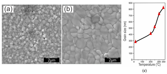
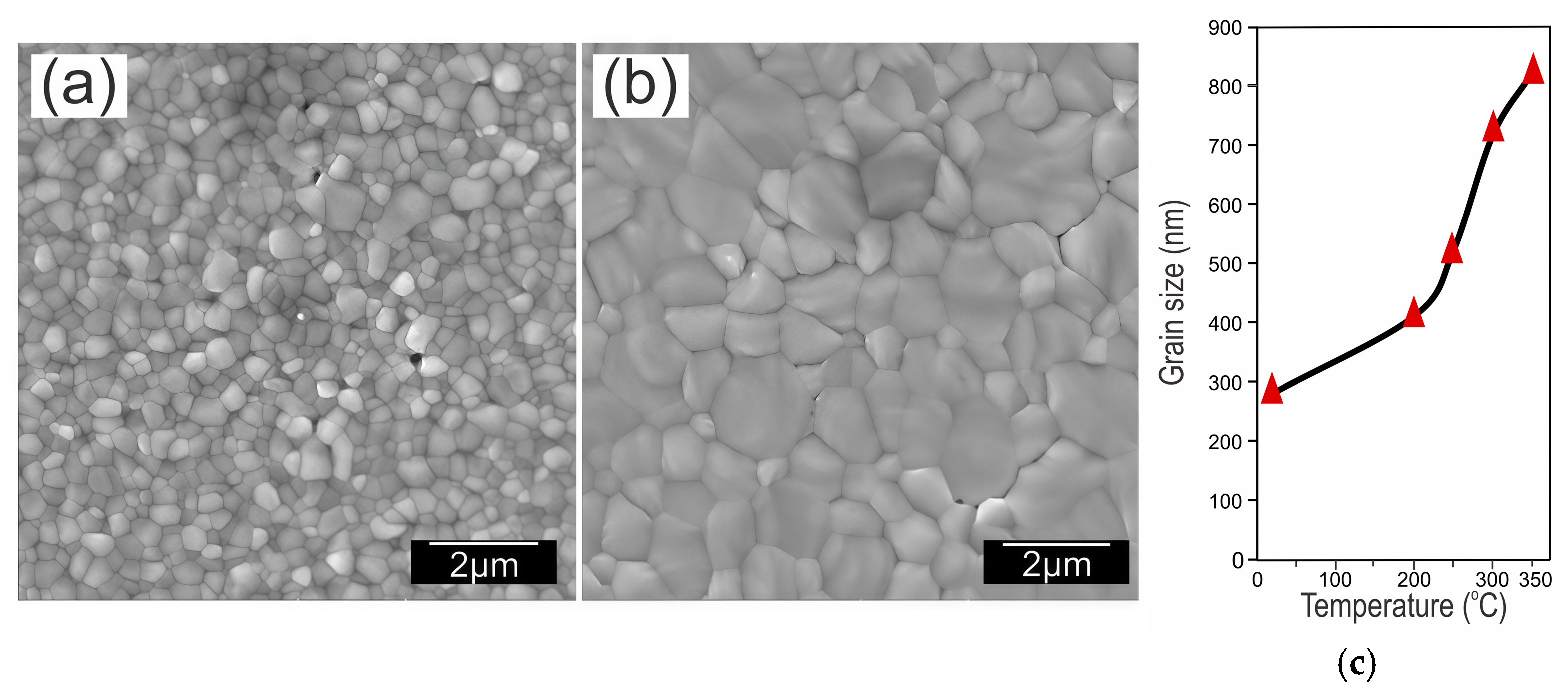
The influence that the partial substitution of Br− by iodine and of Pb2+ by Zn2+ in the crystal structure of CsPbBr3 thin films, as well as the post-deposition annealing in air, produces on the morphological properties of CsPbBr3−xIx thin films was also studied by SEM measurements. Initially, the effect of annealing temperature (in air between 20 °C and 350 °C, for 15 min) on the morphology of single-phase grown CsPbBr3 thin films was studied. Figure 8a shows the SEM image of an unannealed CsPbBr3 thin film, and Figure 8b shows the SEM image of a sample annealed at 350 °C for 15 min; in Figure 8c, the grain size variation of CsPbBr3 films annealed at temperatures between 20 °C and 350 °C. The grain size was calculated from the SEM micrographs using the linear intercept method [41] in ImageJ software, version 1.54g.
Figure 8.
SEM images of: (a) unannealed CsPbBr3 thin film, (b) sample annealed at 350 °C for 15 min. (c) grain size variation of CsPbBr3 films annealed at temperatures between 20 °C, and 350 °C.
The SEM images in Figure 8 show that the CsPbBr3 films generally have a morphology consisting of compact, pore-free spherical grains, resulting in excellent coverage of the entire substrate. It is also observed that the grain size increases significantly with annealing temperature, from average values close to 280 nm to grain sizes on the order of 820 nm. This behavior is attributed to a morphological change induced by an increase in annealing temperature.
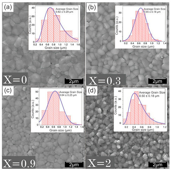
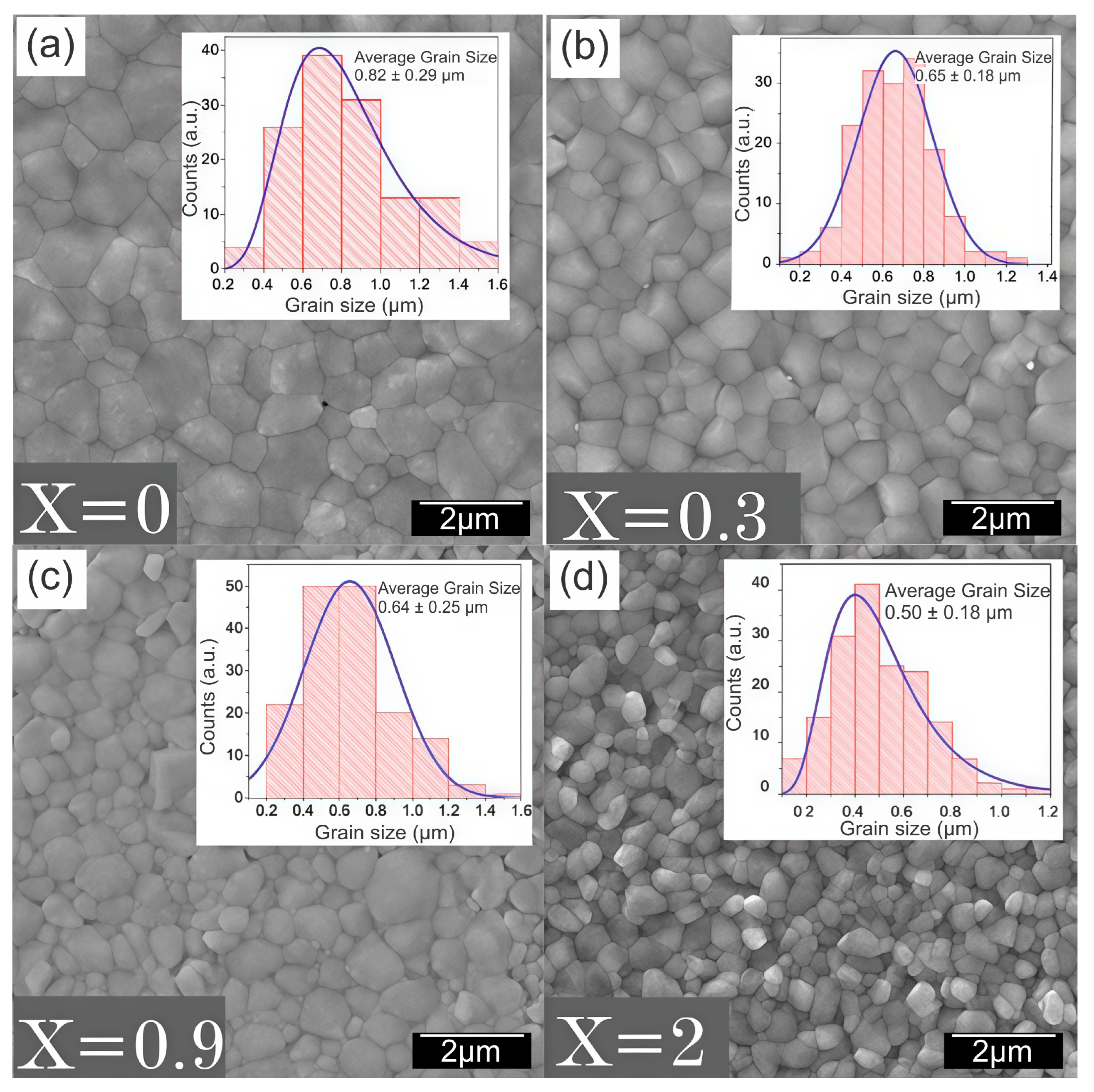
After evaluating the effect of the annealing temperature, the influence of Br−/I− substitution on the film morphology was analyzed. Figure 9 shows SEM micrographs of CsPbBr3−xIx samples prepared with molar ratios ranging from x = 0 to x = 2. These results reveal that all the studied samples exhibit a compact morphology composed of submicrometric, nearly spherical grains. As the iodine content increases from x = 0 to x = 2, the average grain size decreases from 0.82 μm for CsPbBr3 films (Figure 9a) to 0.50 μm for CsPbBrI3 films (Figure 9d).
Figure 9.
SEM images of CsPbBr3−xIx thin films with molar ratios corresponding to: (a) x = 0, (b) x = 0.3, (c) x = 0.9, (d) x = 2.
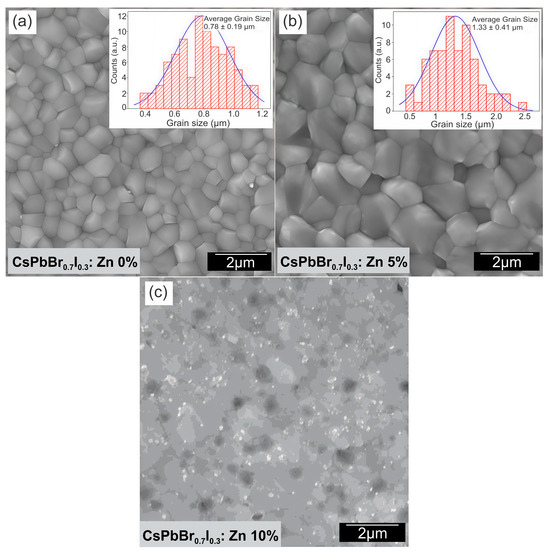
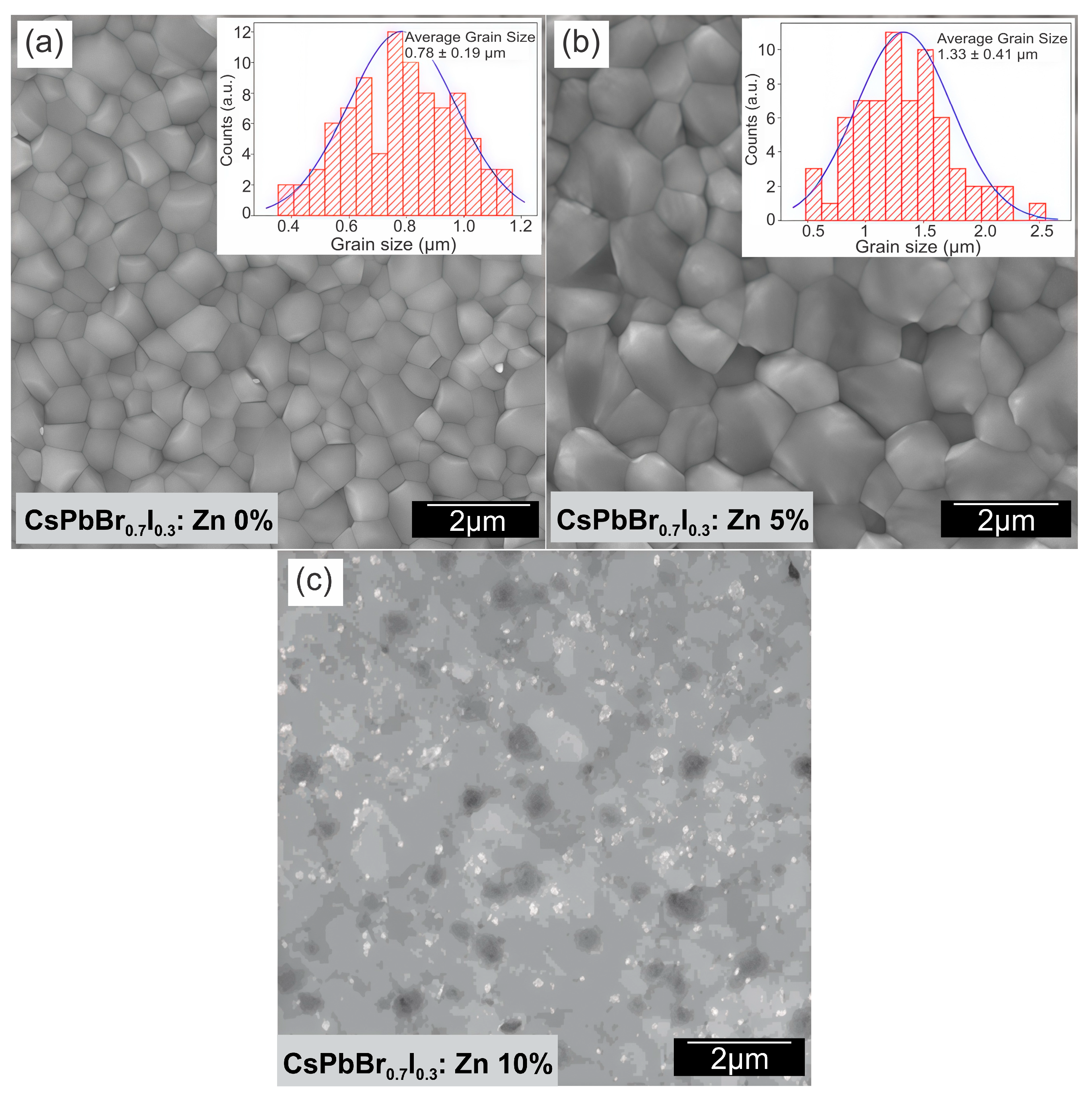
The replacement of the Pb2+ cation by Zn2+ ions in inorganic CsPbBr3−xIx perovskite films is a strategy that has been used effectively to improve both the crystallinity and morphology of this type of compound, as well as the efficiency and stability of cells based on inorganic perovskites [26,30]. In this work, the effect that the replacement of Pb2+ by Zn2+ has on the morphological properties of CsPbBr3−xIx thin films was studied. This study was conducted using a reference sample with molar composition x = 0.3 (CsPbBr2.7I0.3). Figure 10 shows SEM micrographs of the reference sample in which Pb2+ was replaced by Zn2+ at atomic percentages ranging from 0% to 10%. These results reveal that the sample not doped with Zn exhibits a compact, small-grain morphology, and that when the cation Pb2+ is replaced by Zn2+ at low atomic percentages, the grain size increases significantly. When the Pb2+ cation in thin films of CsPbBr2.7I0.3 is substituted in atomic percentages around 5%, samples with grain sizes of 1.33 μm are obtained. Still, when the Pb2+ cation is replaced by Zn2+ in atomic percentages greater than 8%, their morphology deteriorates significantly. These samples show a morphology characterized by the disappearance of the granular structure and the appearance of large islands, with a high density of voids.
Figure 10.
SEM images of a thin film of CsPbBr2.7I0.3 in which Pb was partially replaced by Zn2+ at atomic percentages of: (a) 0%, (b) 5%, and (c) 10%.
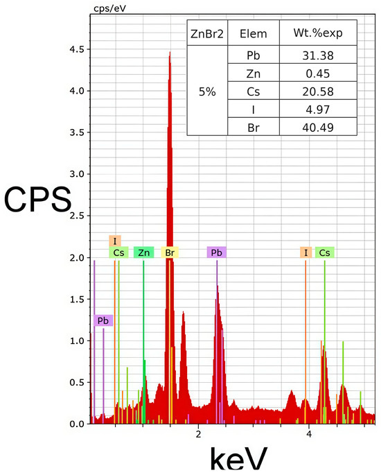
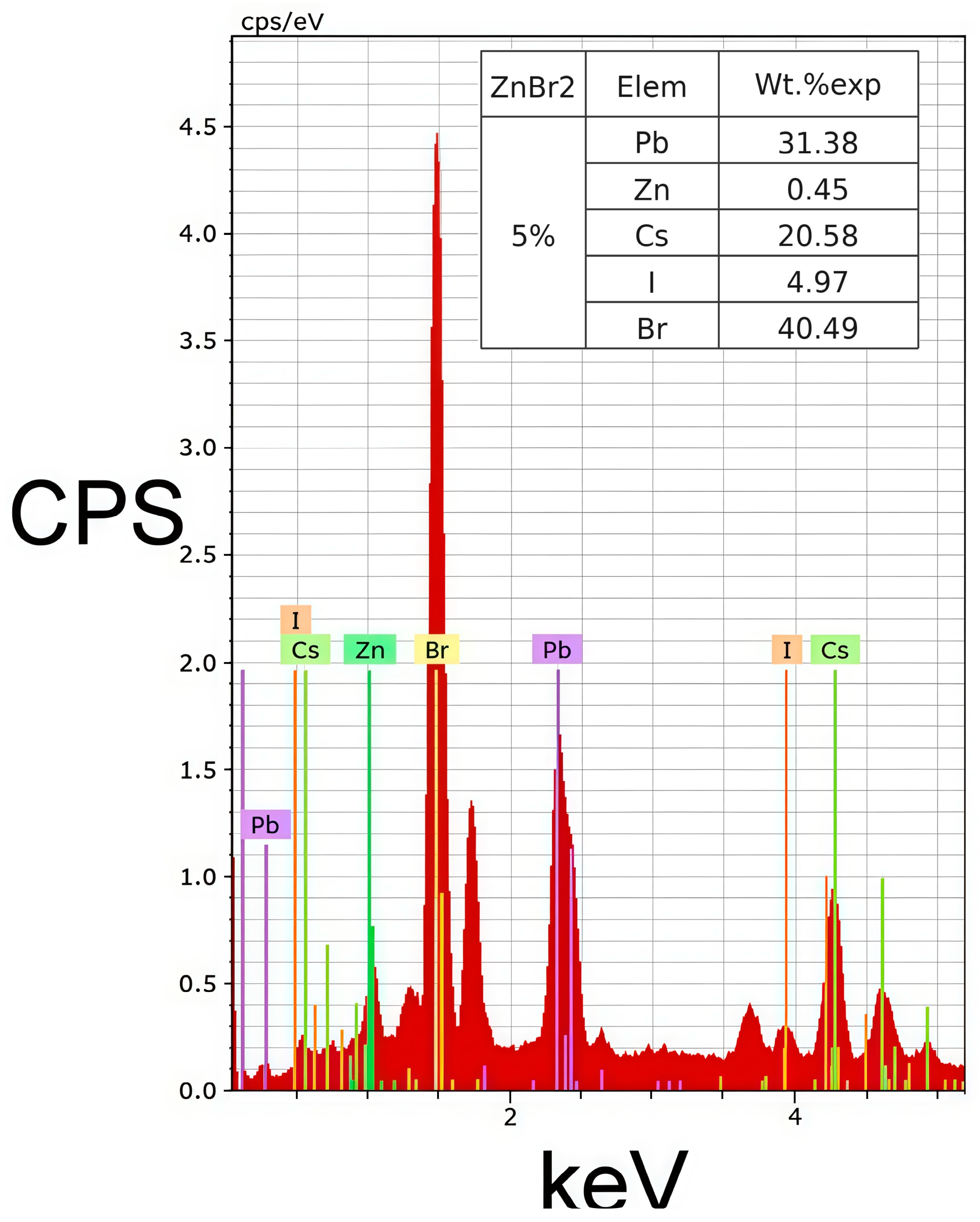
EDX analysis (TESCAN VEGA SEM + EDX) confirmed the incorporation of zinc into the film structure, revealing an experimental concentration of approximately 0.45 wt% Zn (see Figure 11). This result is consistent with the nominal composition used during synthesis, corresponding to a 5% addition of ZnBr2 relative to the Pb content. Considering the total mass of the perovskite and the contributions of the other elements present (Cs, Pb, Br, and I), the expected theoretical Zn content is around 0.5 wt%. Therefore, the agreement between the experimental and theoretical values confirms the effective incorporation of Zn into the synthesized material.
Figure 11.
EDX spectrum of a CsPbBr2.7I0.3 thin film in which Pb2+ was partially replaced by Zn2+ at an atomic percentage of 5%.
3.4. Influence of the Partial Substitution of the Cation Pb2+ by Zn2+ and the Anion Br by Iodine on the Band Structure of CsPbBr3 Films
The influence of the partial substitution of the Pb2+ cation by Zn2+ and the Br− anion by iodine on the band structure of CsPbBr3 perovskites was analyzed through DFT computational calculations. To that end, from the x-ray diffraction patterns of the synthesized films, a supercell was constructed with two types of substitution: 5% of the Pb2+ cation sites by Zn2+ and the Br anion by iodine in a ratio x = 0.3 (CsPbBr2.7I0.3). The minimal supercell corresponded to a 3 × 2 × 1 expansion of the primitive cell, with a total of 120 atoms. The configuration with the largest spacing between iodine atoms was selected to approximate a homogeneous distribution, and the most central Pb atom was substituted to minimize periodic interactions.
Structural relaxation was performed using pw.x from the Quantum ESPRESSO package, version 7.4 [42] and the correlation-exchange functional R2SCAN [43], chosen for its balance between accuracy and computational cost. Subsequently, the band structures were calculated using SCF and NSCF with pw.x [42] and bands.x. On the other hand, the total and projected density of states (DOS) were calculated with dos.x and projwfc.x [42]. Band unfolding was performed using BandUPpy, version 0.3.4 [44], obtaining the effective band structure (EBS) of the primitive cell from the supercell. The results were processed and plotted using GNUPlot, version 5.2 [45], Origin Lab, version 9.8 [46], and Jupyter Notebooks version 7.2 [47].
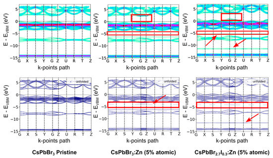
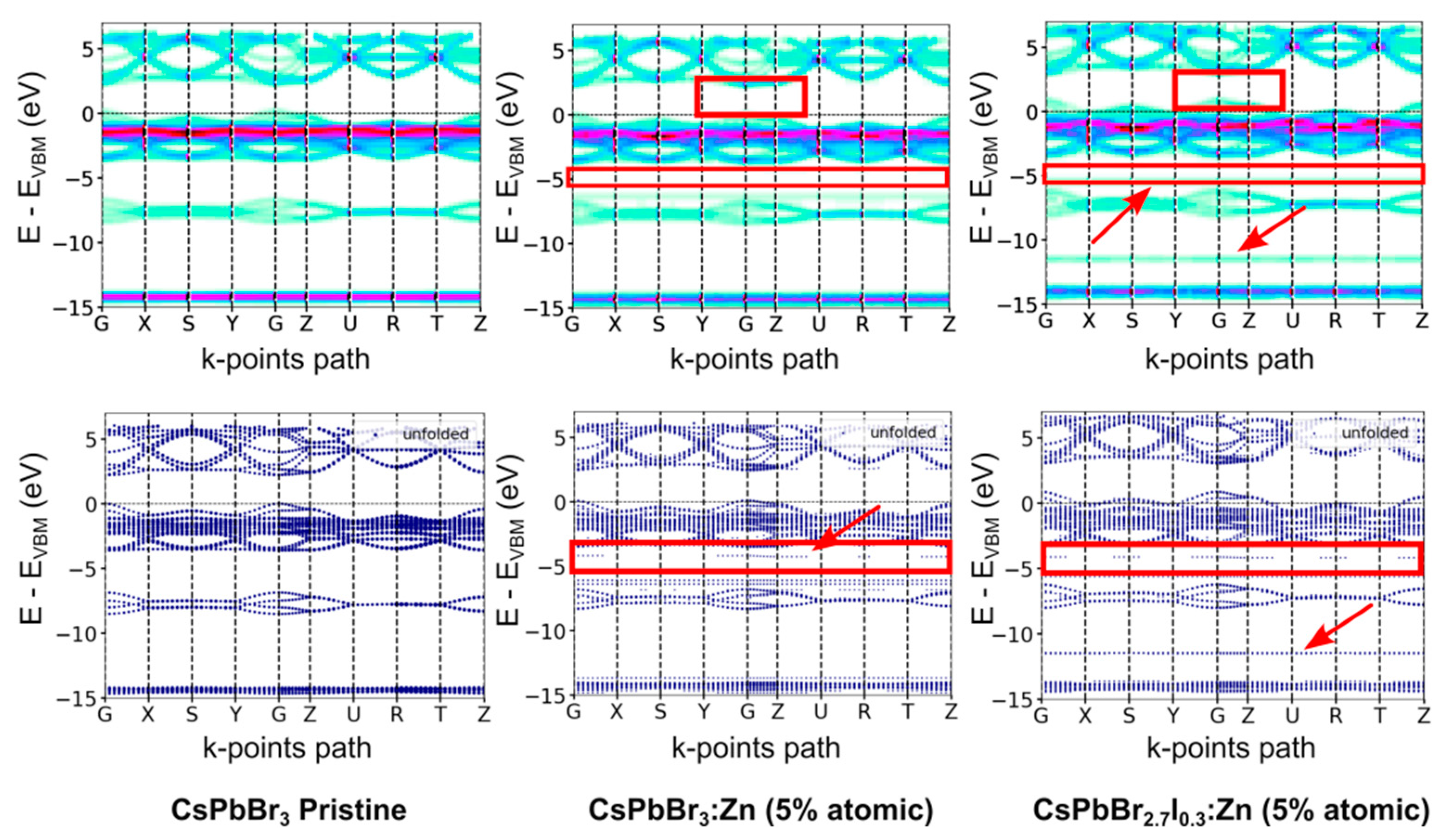
Figure 12 shows the EBSs for pristine CsPbBr3 as well as for Zn2+ and Zn2+ + I−-doped supercells. In all cases, a direct band gap at Γ is preserved, with a slight reduction from 2.20 eV to 2.18 eV, which is in agreement with previous studies on the bandgap stability in halogen- or transition-metal-doped CsPbBr3 [48,49].
Figure 12.
Effective band structures for the CsPbBr3: Zn (5%) (center) and CsPbBr2.7I0.3: Zn (5%) supercells (right). The band structure for the primitive CsPbBr3 cell is shown (left), for reference. The arrows and red boxes highlight the density-of-states contributions arising from the incorporation of Zn and I.
From these results, it was established that the Zn2+ and I− substitutions preserve the direct semiconductor character of CsPbBr3, an essential condition for photovoltaic applications [48,49,50]. Furthermore, the band gap changes very little, thereby preserving the fundamental optical properties [49].
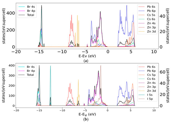
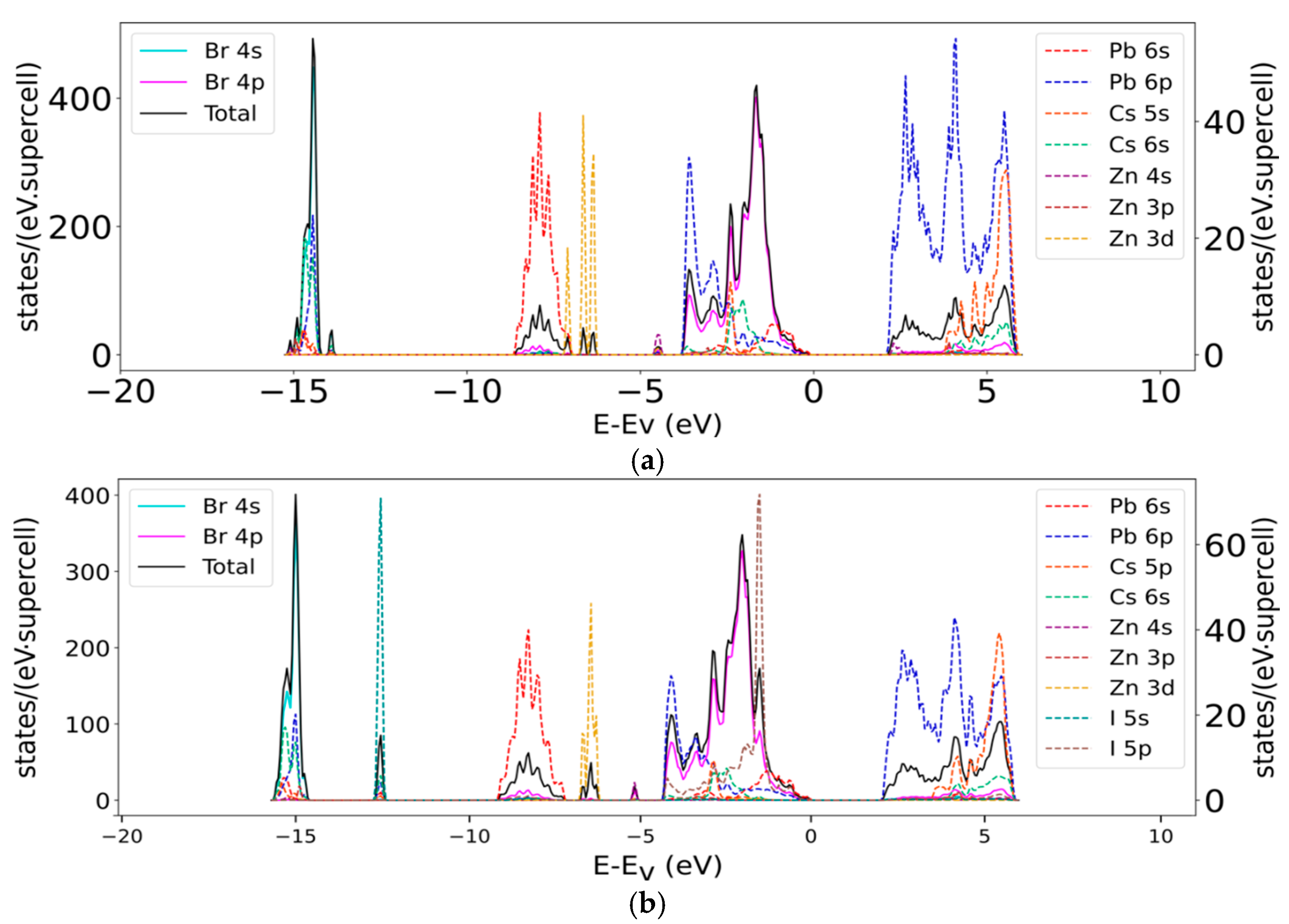
On the other hand, Figure 13 also displays localized states associated with the incorporation of Zn2+. Based on these results, the following facts stand out:
Figure 13.
Density of states projected onto atomic orbitals for the 5% Zn-doped perovskite supercells: (a) CsPbBr3:Zn and (b) CsPbBr2.7I0.3:Zn. The dotted curves correspond to the right vertical axis because of their lower magnitudes.
- −
- The shallow valence bands originate from Br 4p, with minor contributions from I 5p and Pb 6s.
- −
- The deep valence bands include Zn 3d states (~7 eV), Pb 6s, I 5s, and Cs 5p.
- −
- The conduction band is composed primarily of Pb 6p states, with minor contributions from Br 4p and Cs 6s.
- −
- Iodine mainly affects hole transport through contributions to valence states, in agreement with prior studies on mixed-halide perovskites [50]. Zn does not introduce significant states within the band gap, suggesting that excessive Zn doping could reduce the density of available states for carrier generation, as recent studies have also noted [51].
3.5. Influence of Zn Halide Doping on the Performance of Solar Cells Fabricated with FTO/TiO2/CsPbBr2.7I0.3/C Structure
Using as an absorber layer sequentially evaporated CsPbBr2.7I0.3 films, carbon-based planar heterojunction PSCs of 1 cm2 area, with a structure FTO/c-TiO2/CsPbBr2.7I0.3/carbon, were fabricated, placing special emphasis on the evaluation of the effect on the device’s performance of the partial substitution of the Pb2+ cation by Zn2+ in atomic percentages that varied between 0% and 12%. The thickness of the CsPbBr2.7I0.3 absorber layer is about 600 nm, which is similar to that of sequentially evaporated and dual-source co-evaporated CsPbBr3 films used in the manufacture of PSCs [34,52]. c-TiO2 films of about 40 nm-thick, prepared by RF magnetron sputtering, were used as ETL, and a carbon layer prepared from commercial carbon paste was doctor-bladed onto the perovskite absorber layer in ambient air, then dried at 120 °C for 20 min and used as the device counter electrode.
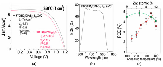
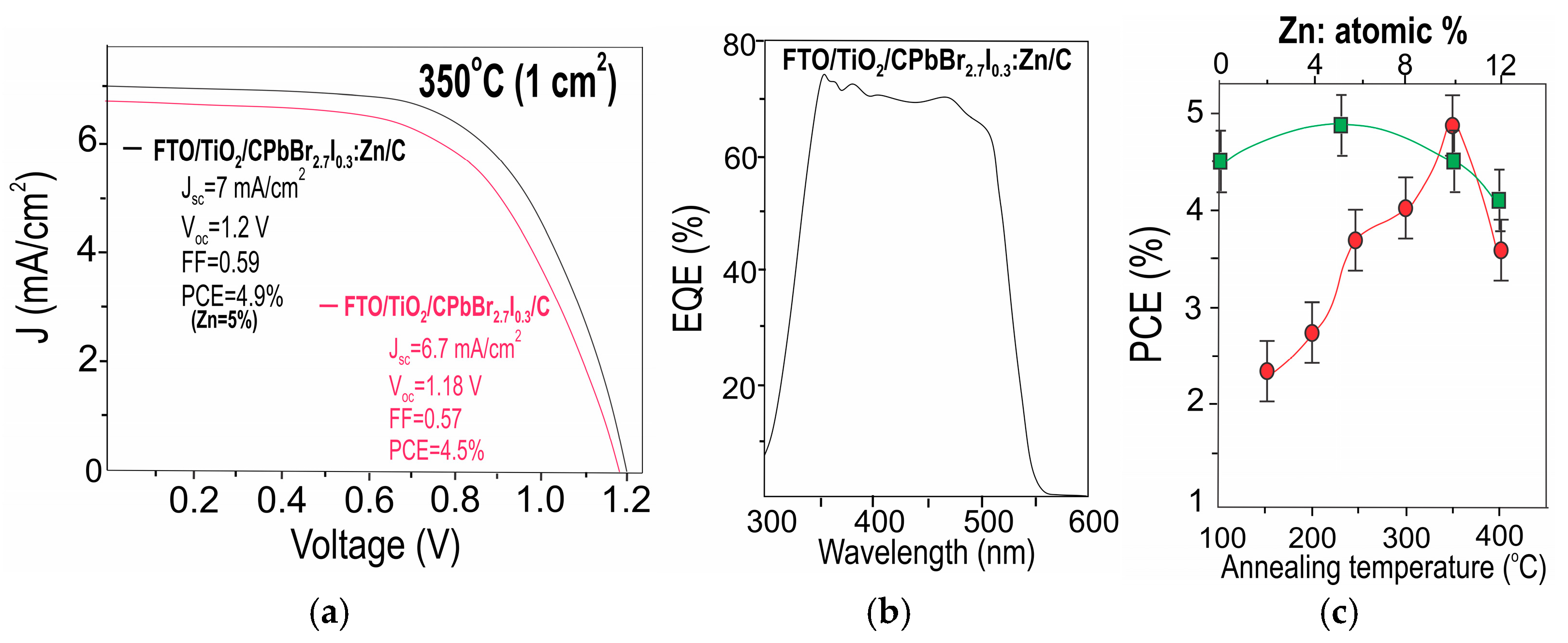
In Figure 14a, the J-V curve of the best-performing device, fabricated with a CsPbBr2.7I0.3 absorber layer, is compared with the J-V curve of the best-performing device, fabricated with a CsPbBr2.7I0.3 film, in which the Pb2+ cation was replaced by Zn2+ at an atomic percentage of 5%. These devices were fabricated with an active area of 1 cm2 and were reverse-recorded under illumination of 100 mW/cm2. The corresponding EQE spectrum and the dependence of PCE on annealing temperature and Zn2+ doping concentration are presented in Figure 14b and Figure 14c, respectively.
Figure 14.
(a) Comparison of the J-V characteristic of the best-performing device fabricated using a 5% Zn2+ doped CsPbBr2.7I0.3 absorber layer with that of a device fabricated using no doped CsPbBr2.7I0.3, (b) EQE spectra of the best Zn2+-doped solar cell with area of 1 cm2 and (c) PCE as a function of annealing temperature in air (red line) and atomic percentage of Zn2+ doping of CsPbBr2.7I0.3 (green line)-based solar cells.
The 5% Zn2+-doped perovskite film-based device achieved a champion PCE of 4.9%, with a Jsc of 7 mA/cm2, a Voc of 1.2 V, and a FF of 0.59. On the other hand, no Zn-doped perovskite film-based device exhibited a champion PCE of 4.5%, with a Jsc of 6.7 mA/cm2, a Voc of 1.18 V and a FF of 0.57.
In Figure 13b, the external quantum efficiency (EQE) of the best solar cell (5% Zn2+ doped) is depicted. It exhibits a high response of photons in the wavelength range 300–530 nm and a cut-off wavelength around 530 nm, in agreement with the cut-off wavelength of transmittance spectrum of the 5%-doped, absorber CsPbBr2.7I0.3 layer (see Figure 6a). In Figure 14c is displayed a curve of the PCE as a function of both annealing temperature in air and atomic percentage of Zn2+ doping of CsPbBr2.7I0.3-based solar cells. It is observed that device efficiency increases with annealing temperature up to 350 °C, but performance deteriorates at higher annealing temperatures. Efficiency also increases slightly upon substituting Pb2+ for Zn2+ at atomic percentages between 0% and 5%. However, it decreases sharply when the substitution of Pb2+ for Zn2+ exceeds 5%.
The results presented in Figure 14 allow us to conclude that the highest PCE values were obtained for cells manufactured using, as the absorber layer, cesium lead bromide iodide mixed perovskite thin films doped with 5% Zn2+ and annealed at 350 °C in air. The optimal performance of the cells fabricated under the aforementioned conditions of doping with Zn2+ and annealing in air is apparently attributed to the fact that the replacement of the Pb2+ cation by Zn2+ ions in inorganic CsPbBr3−xIx perovskite films effectively improves both the crystallinity and morphology of this type of compounds, which lead to an improvement in the performance of the device.
4. Conclusions
In this paper, contributions were made related to the growth of thin films of cesium lead bromide iodide mixed perovskite (CsPbBr3−xIx), synthesized by sequential evaporation of precursors (CsBr, PbBr2, PbI2). High-quality CsPbBr3−xIx films were achieved by accurately tuning the thickness ratio using an electronic system that automatically controlled the deposition process via PID and PWM algorithms. A significant improvement in the morphology and crystallinity of the CsPbBr3−xIx films was achieved by both post-deposition annealing at temperatures around 350 °C and Zn2+ halide doping. In general, samples not doped with Zn2+ present a morphology consisting of compact small grains, and when the Pb2+ cation is replaced by Zn2+ in small atomic percentages, the grain size increases significantly. Grain sizes around 1.33 μm can be achieved with CsPbBr2.7I0.3 films by substituting the Pb2+ cation with Zn2+ at atomic percentages around 5%.
The influence of the partial substitution of the Pb2+ cation by Zn2+ and the Br− anion by iodine on the band structure and density of localized states associated with CsPbBr3 perovskites was analyzed through DFT computational calculations, using the Quantum ESPRESSO package and the correlation-exchange functional R2SCAN. From these results, it was established that the Zn2+ and I− substitutions preserve the direct semiconductor character of CsPbBr3, with only minor variations in the band gap. The results also indicate that the conduction band is primarily composed of Pb 6p states, whereas the shallow valence bands originate primarily from Br 4p, and that the deep valence bands include Zn 3d, Pb 6s, I 5s, and Cs 5p states.
Carbon-based planar solar cells with FTO/c-TiO2/CsPbBr2.7I0.3/carbon structure were fabricated, and the effects of annealing temperature and Zn2+ doping on the quality of a reference CsPbBr2.7I0.3 film and its photovoltaic performance were studied. The highest PCE values are obtained with cells manufactured using thin films of CsPbBr2.7I0.3 that substitute Zn2+ for Pb2+ at 5% Zn2+ and are annealed at 350 °C in air as the absorber layer. This result is apparently due to a significant improvement in crystallinity and morphology observed in inorganic perovskite films when they are annealed at high temperatures, and the Pb cation is substituted by Zn2+ ions.
Author Contributions
Conceptualization, J.I.C.; Formal analysis, J.Z.G.-N.; Investigation, O.G.T.; Data curation, J.A.A.-E.; Writing—original draft, J.C.P.-B.; Supervision, G.G. All authors have read and agreed to the published version of the manuscript.
Funding
This research received no external funding.
Data Availability Statement
The raw data supporting the conclusions of this article will be made available by the authors on request.
Acknowledgments
This study was supported by the DIEB-Universidad Nacional de Colombia (proy. 59845), Sede Bogotá, Facultad de Ciencias, Departamento de Física, Grupo de Materiales Semiconductores y Energía Solar, K30 #45-03, Bogotá DC, Colombia.
Conflicts of Interest
The authors declare no conflicts of interest.
Abbreviations
The following abbreviations are used in this manuscript:
| Abbreviation | Definition |
| NREL | National Renewable Energy Laboratory |
| EPFL | Swiss Federal Institute of Technology in Lausanne |
| PV | Photovoltaic |
| PSCs | Perovskite solar cells |
| PID | Proportional–Integral–Derivative |
| PWM | Pulse Width Modulation |
| Eg | Energy gap |
| EU | Urbach energy |
| EBS | Effective band structure |
| ETL | Electron transport layer |
| EQE | External quantum efficiency |
| PCE | Power conversion efficiency |
| XRD | X-ray diffraction |
| SEM | Scanning electron microscopy |
| DFT | Density functional theory |
References
- Ansari, M.I.H.; Qurashi, A.; Nazeeruddin, M.K. Frontiers, opportunities, and challenges in perovskite solar cells: A critical review. J. Photochem. Photobiol. C Photochem. Rev. 2018, 35, 1–24. [Google Scholar] [CrossRef] [Scilit]
- Zhang, S.; Li, Y.; Huang, J.; Li, S.; Wang, Z.; Peng, Z.; Chen, J.; Chen, J. Interface modification of imidazolium ionic liquid toward efficient and stable carbon-electroded CsPbI2Br perovskite solar cells. J. Power Sources 2025, 660, 238495. [Google Scholar] [CrossRef] [Scilit]
- Xing, G.; Mathews, N.; Lim, S.S.; Yantara, N.; Liu, X.; Sabba, D.; Grätzel, M.; Mhaisalkar, S.; Sum, T.C. Long-Range Balanced Electron- and Hole-Transport Lengths in Organic-Inorganic CH3NH3PbI3. Science 2013, 342, 344–347. [Google Scholar] [CrossRef] [Scilit] [PubMed]
- Xu, H.; Guo, Z.; Chen, P.; Wang, S. Toward durable all-inorganic perovskite solar cells: From lead-based to lead-free. Chem. Commun. 2024, 60, 12287–12301. [Google Scholar] [CrossRef] [Scilit] [PubMed]
- Brenner, T.M.; Egger, D.A.; Kronik, L.; Hodes, G.; Cahen, D. Hybrid organic—Inorganic perovskites: Low-cost semiconductors with intriguing charge-transport properties. Nat. Rev. Mater. 2016, 1, 15007. [Google Scholar] [CrossRef] [Scilit]
- Stranks, S.D.; Eperon, G.E.; Grancini, G.; Menelaou, C.; Alcocer, M.J.P.; Leijtens, T.; Herz, L.M.; Petrozza, A.; Snaith, H.J. Electron-Hole Diffusion Lengths Exceeding 1 Micrometer in an Organometal Trihalide Perovskite Absorber. Science 2013, 342, 341–344. [Google Scholar] [CrossRef] [Scilit] [PubMed]
- Noman, M.; Khan, Z.; Jan, S.T. A comprehensive review on the advancements and challenges in perovskite solar cell technology. RSC Adv. 2024, 14, 5085–5131. [Google Scholar] [CrossRef] [Scilit] [PubMed]
- Dong, Q.; Fang, Y.; Shao, Y.; Mulligan, P.; Qiu, J.; Cao, L.; Huang, J. Electron-hole diffusion lengths > 175 μm in solution-grown CH3NH3PbI3 single crystals. Science 2015, 347, 967–970. [Google Scholar] [CrossRef] [Scilit] [PubMed]
- Tian, W.; Wang, R.; Yang, D.; Xue, J. Organic A-cations in metal halide perovskite photovoltaics. Nat. Rev. Chem. 2026, 10, 50–71. [Google Scholar] [CrossRef] [Scilit] [PubMed]
- Wang, J.; Wei, Y.; Xu, Y.; Wang, Q.; Lu, H.; Qiu, L.; Zhu, J. Photoluminescence and electroluminescence properties of aligned CsPbBr3 nanowire films prepared by off-center spin-coating. Synth. Met. 2020, 267, 116481. [Google Scholar] [CrossRef] [Scilit]
- Green, M.A.; Dunlop, E.D.; Yoshita, M.; Kopidakis, N.; Bothe, K.; Siefer, G.; Hinken, D.; Rauer, M.; Hohl-Ebinger, J.; Hao, X. Solar cell efficiency tables (Version 64). Prog. Photovolt. Res. Appl. 2024, 32, 425–441. [Google Scholar] [CrossRef] [Scilit]
- Green, M.A.; Dunlop, E.D.; Hohl-Ebinger, J.; Yoshita, M.; Kopidakis, N.; Ho-Baillie, A.W.Y. Solar cell efficiency tables (Version 55). Prog. Photovolt. Res. Appl. 2020, 28, 3–15. [Google Scholar] [CrossRef] [Scilit]
- Park, N.-G. Organometal Perovskite Light Absorbers Toward a 20% Efficiency Low-Cost Solid-State Mesoscopic Solar Cell. J. Phys. Chem. Lett. 2013, 4, 2423–2429. [Google Scholar] [CrossRef] [Scilit]
- Interactive Best Research-Cell Efficiency Chart|Photovoltaic Research|NREL. Available online: https://www.nrel.gov/pv/interactive-cell-efficiency (accessed on 14 December 2025).
- 34.6%! Record-Breaker LONGi Once Again Sets a New World Efficiency for Silicon-Perovskite Tandem Solar Cells. Available online: https://www.longi.com/en/news/2024-snec-silicon-perovskite-tandem-solar-cells-new-world-efficiency/ (accessed on 14 December 2025).
- Rijal, B.; Alzoubi, K.M.; Chen, Z.; Khammash, A.L.; Lu, S.; Dhakal, T.P. Understanding the Long-Term Instability in Perovskite Solar Cells: Mechanisms and Mitigation Strategies. Electronics 2025, 14, 4428. [Google Scholar] [CrossRef] [Scilit]
- Manser, J.S.; Saidaminov, M.I.; Christians, J.A.; Bakr, O.M.; Kamat, P.V. Making and Breaking of Lead Halide Perovskites. Acc. Chem. Res. 2016, 49, 330–338. [Google Scholar] [CrossRef] [Scilit] [PubMed]
- Zhou, W.; Zhao, Y.; Zhao, Q. Ionic transport in perovskite semiconductors. In Halide Perovskite Semiconductors: Structures, Characterization, Properties, and Phenomena; Wiley: Hoboken, NJ, USA, 2023; pp. 305–328. [Google Scholar] [CrossRef] [Scilit]
- Lau, C.F.J.; Deng, X.; Ma, Q.; Zheng, J.; Yun, J.S.; Green, M.A.; Huang, S.; Ho-Baillie, A.W.Y. CsPbIBr2 Perovskite Solar Cell by Spray-Assisted Deposition. ACS Energy Lett. 2016, 1, 573–577. [Google Scholar] [CrossRef] [Scilit]
- Sutton, R.J.; Eperon, G.E.; Miranda, L.; Parrott, E.S.; Kamino, B.A.; Patel, J.B.; Hörantner, M.T.; Johnston, M.B.; Haghighirad, A.A.; Moore, D.T.; et al. Bandgap-Tunable Cesium Lead Halide Perovskites with High Thermal Stability for Efficient Solar Cells. Adv. Energy Mater. 2016, 6, 1502458. [Google Scholar] [CrossRef] [Scilit]
- Dey, A.; Ye, J.; De, A.; Debroye, E.; Ha, S.K.; Bladt, E.; Kshirsagar, A.S.; Wang, Z.; Yin, J.; Wang, Y.; et al. State of the Art and Prospects for Halide Perovskite Nanocrystals. ACS Nano 2021, 15, 10775–10981. [Google Scholar] [CrossRef] [Scilit] [PubMed]
- Shen, C.; Ye, T.; Yang, P.; Chen, G. All–Inorganic Perovskite Solar Cells: Defect Regulation and Emerging Applications in Extreme Environments. Adv. Mater. 2024, 36, 2401498. [Google Scholar] [CrossRef] [Scilit] [PubMed]
- Wang, Z.; Tian, Q.; Zhang, H.; Xie, H.; Du, Y.; Liu, L.; Feng, X.; Najar, A.; Ren, X.; Liu, S. Managing Multiple Halide-Related Defects for Efficient and Stable Inorganic Perovskite Solar Cells. Angew. Chem. Int. Ed. 2023, 62, e202305815. [Google Scholar] [CrossRef] [Scilit] [PubMed]
- Liang, J.; Liu, Z.; Qiu, L.; Hawash, Z.; Meng, L.; Wu, Z.; Jiang, Y.; Ono, L.K.; Qi, Y.B. Enhancing Optical, Electronic, Crystalline, and Morphological Properties of Cesium Lead Halide by Mn Substitution for High-Stability All-Inorganic Perovskite Solar Cells with Carbon Electrodes. Adv. Energy Mater. 2018, 8, 1800504. [Google Scholar] [CrossRef] [Scilit]
- Liu, P.; Yang, X.; Chen, Y.; Xiang, H.; Wang, W.; Ran, R.; Zhou, W.; Shao, Z. Promoting the Efficiency and Stability of CsPbIBr2-Based All-Inorganic Perovskite Solar Cells through a Functional Cu2+ Doping Strategy. ACS Appl. Mater. Interfaces 2020, 12, 23984–23994. [Google Scholar] [CrossRef] [Scilit] [PubMed]
- Wang, G.; Lei, M.; Liu, J.; He, Q.; Zhang, W. Improving the Stability and Optoelectronic Properties of All Inorganic Less-Pb Perovskites by B-Site Doping for High-Performance Inorganic Perovskite Solar Cells. Sol. RRL 2020, 4, 2000528. [Google Scholar] [CrossRef] [Scilit]
- Subhani, W.S.; Wang, K.; Du, M.; Liu, S.F. Goldschmidt-rule-deviated perovskite CsPbIBr2 by barium substitution for efficient solar cells. Nano Energy 2019, 61, 165–172. [Google Scholar] [CrossRef] [Scilit]
- Sun, H.; Zhang, J.; Gan, X.; Yu, L.; Yuan, H.; Shang, M.; Lu, C.; Hou, D.; Hu, Z.; Zhu, Y.; et al. Pb-Reduced CsPb0.9Zn0.1I2Br Thin Films for Efficient Perovskite Solar Cells. Adv. Energy Mater. 2019, 9, 1900896. [Google Scholar] [CrossRef] [Scilit]
- Bi, C.; Sun, X.; Huang, X.; Wang, S.; Yuan, J.; Wang, J.X.; Pullerits, T.; Tian, J. Stable CsPb1−xZnxI3 Colloidal Quantum Dots with Ultralow Density of Trap States for High-Performance Solar Cells. Chem. Mater. 2020, 32, 6105–6113. [Google Scholar] [CrossRef] [Scilit]
- Chen, Z.; Wang, Q.; Xu, Y.; Zhang, L.; Yang, A.; Zhou, R.; Lu, H.; Lyu, M.; Zhu, J. Enhancing the performance of CsPbIBr2 solar cells through zinc halides doping. Synth. Met. 2021, 281, 116918. [Google Scholar] [CrossRef] [Scilit]
- Long, Y.; Wang, C.; Liu, X.; Wang, J.; Fu, S.; Zhang, J.; Hu, Z.; Zhu, Y. Zinc ion functional doping for all-inorganic planar CsPbIBr2 perovskite solar cells with efficiency over 10.5%. J. Mater. Chem. C 2021, 9, 2145–2155. [Google Scholar] [CrossRef] [Scilit]
- Reinoso, M.; Otálora, C.A.; Gordillo, G. Improvement properties of hybrid Halide perovskite thin films prepared by sequential evaporation for planar solar cells. Materials 2019, 12, 1394. [Google Scholar] [CrossRef] [Scilit] [PubMed]
- Xiang, T.; Zhang, Y.; Wu, H.; Li, J.; Yang, L.; Wang, K.; Xia, J.; Deng, Z.; Xiao, J.; Li, W.; et al. Universal defects elimination for high performance thermally evaporated CsPbBr3 perovskite solar cells. Sol. Energy Mater. Sol. Cells 2020, 206, 110317. [Google Scholar] [CrossRef] [Scilit]
- Liu, X.; Tan, X.; Liu, Z.; Sun, B.; Li, J.; Xi, S.; Shi, T.; Liao, G. Sequentially vacuum evaporated high-quality CsPbBr3 films for efficient carbon-based planar heterojunction perovskite solar cells. J. Power Sources 2019, 443, 227269. [Google Scholar] [CrossRef] [Scilit]
- Duan, J.; Zhao, Y.; He, B.; Tang, Q. High-Purity Inorganic Perovskite Films for Solar Cells with 9.72% Efficiency. Angew. Chem. Int. Ed. 2018, 57, 3787–3791. [Google Scholar] [CrossRef] [Scilit] [PubMed]
- Ruske, F.; Wimmer, M.; Köppel, G.; Pflug, A.; Rech, B. Optical characterization of high mobility polycrystalline ZnO:Al films. Proc. SPIE 2012, 8263, 826303. [Google Scholar] [CrossRef] [Scilit]
- Kurik, M.V. Urbach rule. Phys. Status Solidi A 1971, 8, 9–45. [Google Scholar] [CrossRef] [Scilit]
- Shannon, R.D. Revised effective ionic radii and systematic studies of interatomic distances in halides and chalco-genides. Acta Crystallogr. Sect. A 1976, 32, 751–767. [Google Scholar] [CrossRef] [Scilit]
- Ng, C.H.; Ripolles, T.S.; Hamada, K.; Teo, S.H.; Lim, H.N.; Bisquert, J.; Hayase, S. Tunable Open Circuit Voltage by Engineering Inorganic Cesium Lead Bromide/Iodide Perovskite Solar Cells. Sci. Rep. 2018, 8, 2482. [Google Scholar] [CrossRef] [Scilit] [PubMed]
- Han, Y.; Zhao, H.; Duan, C.; Yang, S.; Yang, Z.; Liu, Z.; Liu, S.F. Controlled n-Doping in Air-Stable CsPbI2Br Perovskite Solar Cells with a Record Efficiency of 16.79%. Adv. Funct. Mater. 2020, 30, 1909972. [Google Scholar] [CrossRef] [Scilit]
- ASTM E112-24; Standard Test Methods for Determining Average Grain Size. ASTM International: West Conshohocken, PA, USA, 2024.
- Giannozzi, P.; Baroni, S.; Bonini, N.; Calandra, M.; Car, R.; Cavazzoni, C.; Ceresoli, D.; Chiarotti, G.L.; Cococcioni, M.; Dabo, I.; et al. QUANTUM ESPRESSO: A modular and open-source software project for quantum simulations of materials. J. Phys. Condens. Matter 2009, 21, 395502. [Google Scholar] [CrossRef] [Scilit] [PubMed]
- Furness, J.W.; Kaplan, A.D.; Ning, J.; Perdew, J.P.; Sun, J. Accurate and Numerically Efficient r2SCAN Meta-Generalized Gradient Approximation. J. Phys. Chem. Lett. 2020, 11, 8208–8215. [Google Scholar] [CrossRef] [Scilit] [PubMed]
- Medeiros, P.V.C.; Stafström, S.; Björk, J. Effects of extrinsic and intrinsic perturbations on the electronic structure of graphene: Retaining an effective primitive cell band structure by band unfolding. Phys. Rev. B 2014, 89, 041407. [Google Scholar] [CrossRef] [Scilit]
- Gnuplot 5.2 an Interactive Plotting Program Thomas Williams & Colin Kelley-DocsLib. Available online: https://docslib.org/doc/5650540/gnuplot-5-2-an-interactive-plotting-program-thomas-williams-colin-kelley#google_vignette (accessed on 15 December 2025).
- OriginLab—Origin and OriginPro—Data Analysis and Graphing Software. Available online: https://www.originlab.com/ (accessed on 15 December 2025).
- Kluyver, T.; Ragan-Kelley, B.; Perez, F.; Granger, B.; Bussonnier, M.; Frederic, J.; Kelley, K.; Hamrick, J.; Grout, J.; Corlay, S.; et al. Jupyter Notebooks—A publishing format for reproducible computational workflows. In Positioning and Power in Academic Publishing: Players, Agents and Agendas; 20th International Conference on Electronic Publishing, ELPUB 2016; IOS Press: Amsterdam, The Netherlands, 2016; pp. 87–90. [Google Scholar] [CrossRef] [Scilit]
- Even, J.; Pedesseau, L.; Katan, C. Analysis of Multivalley and Multibandgap Absorption and Enhancement of Free Carriers Related to Exciton Screening in Hybrid Perovskites. J. Phys. Chem. C 2014, 118, 11566–11572. [Google Scholar] [CrossRef] [Scilit]
- Huang, T.; Zou, B. Luminescent Behavior of Sb3+-Activated Luminescent Metal Halide. Nanomaterials 2023, 13, 2867. [Google Scholar] [CrossRef] [Scilit] [PubMed]
- Kim, G.Y.; Senocrate, A.; Wang, Y.R.; Moia, D.; Maier, J. Photo-Effect on Ion Transport in Mixed Cation and Halide Perovskites and Implications for Photo-Demixing. Angew. Chem. Int. Ed. 2021, 60, 820–826. [Google Scholar] [CrossRef] [Scilit] [PubMed]
- VanOrman, Z.A.; Sullivan, C.M.; Yang, C.W.; Isokuortti, J.; Nienhaus, L. Lead the Way: Halide Perovskites as Next-Generation Triplet Sensitizers for Photon Upconversion. Chem. Rev. 2025, 125, 11426–11460. [Google Scholar] [CrossRef] [Scilit] [PubMed]
- Lei, J.; Gao, F.; Wang, H.; Li, J.; Jiang, J.; Wu, X.; Gao, R.; Yang, Z.; Liu, S.F. Efficient planar CsPbBr3 perovskite solar cells by dual-source vacuum evaporation. Sol. Energy Mater. Sol. Cells 2018, 187, 1–8. [Google Scholar] [CrossRef] [Scilit]
Disclaimer/Publisher’s Note: The statements, opinions and data contained in all publications are solely those of the individual author(s) and contributor(s) and not of MDPI and/or the editor(s). MDPI and/or the editor(s) disclaim responsibility for any injury to people or property resulting from any ideas, methods, instructions or products referred to in the content. |
© 2026 by the authors. Licensee MDPI, Basel, Switzerland. This article is an open access article distributed under the terms and conditions of the Creative Commons Attribution (CC BY) license.