Article

Loss Analysis of P3 Laser Patterning of Perovskite Solar Cells via Hyperspectral Photoluminescence Imaging

1
School of Engineering–Energy and Information, HTW Berlin—University of Applied Sciences, Wilhelminenhofstr. 75a, D-12459 Berlin, Germany
2
Photon etc., 5795 Av. de Gaspé, #222, Montréal, QC H2S 2X3, Canada
3
Young Investigator Group Hybrid Materials Formation and Upscaling, Helmholtz-Zentrum Berlin für Materialien und Energie, Kekuléstr. 5, D-12489 Berlin, Germany
4
Competence Centre Photovoltaics Berlin (PVcomB), Helmholtz-Zentrum Berlin für Materialien und Energie, Schwarzschildstr. 3, D-12489 Berlin, Germany
*
Authors to whom correspondence should be addressed.
These authors contributed equally.
Solar 2025, 5(2), 13; https://doi.org/10.3390/solar5020013
Submission received: 31 December 2024 / Revised: 18 March 2025 / Accepted: 28 March 2025 / Published: 11 April 2025
(This article belongs to the Special Issue Developments in Perovskite Solar Cells)

Abstract

:
Upscaling perovskite solar cells and modules requires precise laser patterning for series interconnection and spatial characterization of cell parameters to understand laser–material interactions and their impact on performance. This study investigates the use of nanosecond (ns) and picosecond (ps) laser pulses at varying fluences for the P3 patterning step of perovskite solar cells. Hyperspectral photoluminescence (PL) imaging was employed to map key parameters such as optical bandgap energy, Urbach energy, and shunt resistance. The mappings were correlated with electrical measurements, revealing that both ns and ps lasers can be utilized for effective series interconnections with minimal performance losses at optimized fluences. Our findings provide a deeper understanding of fluence-dependent effects in P3 patterning. Moreover, the results demonstrate that the process window is robust, allowing for reasonable cell performance even with deviations from optimal parameters. This robustness, coupled with the scalability of the laser patterning process, emphasize its suitability for industrial module production.

1. Introduction

Organic–inorganic metal halide perovskites (MHPs) have emerged as a leading absorber material for producing high-efficiency solar cells at potentially low costs. These perovskites offer excellent optoelectronic properties, including a high absorption coefficient (104–105 cm−1), long charge carrier diffusion lengths, low recombination rates, and high defect tolerance, making them highly suitable for photovoltaics [1,2]. Laboratory-scale perovskite solar cells (PSCs) have achieved power conversion efficiencies (PCE) exceeding 26%, rivaling the performance of high-end crystalline silicon cells [3].
Beyond their application in photovoltaics, MHPs also demonstrate versatility in optoelectronics, enabling advancements in fields such as microfabrication and photonics [4,5]. Techniques such as femtosecond or direct laser writing enable the precise patterning of perovskite structures and open up applications in multicolor displays, photodetectors, and light-emitting devices by making use of unique material properties such as halide ion migration and phase separation [4,5]. Furthermore, laser technologies such as laser-induced nucleation, annealing, and ablation have proven to be highly compatible with perovskite materials, offering precise control over their properties and enabling new avenues for device fabrication [6].
Despite these advancements, significant challenges remain in commercializing PSCs, particularly in scaling up to industrially relevant sizes. Larger perovskite solar modules (PSMs) often experience efficiency losses due to challenges in maintaining uniform perovskite film quality and ensuring process stability during upscaling, which currently hinders mass production [7].
Another major challenge is the development of precise laser-based patterning processes for monolithic series interconnection, which minimizes electrical losses by maintaining low currents and adding voltages of adjacent cells. In these processes, layers are alternately deposited and patterned with the laser, which are referred to as steps P1, P2, and P3. The P1 and P3 steps electrically isolate the front and back contacts of neighboring cells, while P2 opens the absorber and charge transport layers, creating an electrical pathway between the cells [8]. Pulsed lasers are preferred for these processes because they enable non-contact operation and offer high precision [9,10,11]. However, the thermal sensitivity of perovskite materials presents a significant challenge. Excess laser energy, particularly at pulse overlaps or scribe edges, can damage the material and cause electrical losses. Thus, precise energy control is essential to preserve material properties during patterning [8,11].
Building on our previous work, where we first investigated the fluence dependence in P3 patterning [12] and later established hyperspectral photoluminescence (PL) imaging as an imaging method for extracting solar cell parameters [13], the present study combines both aspects. We employ hyperspectral PL imaging to analyze the fluence dependence of laser-scribed P3 lines, providing insights into the impact of different fluences on both material properties and electrical performance.
Photoluminescence (PL) measurements have proven valuable for analyzing material properties in this context [14,15,16,17,18]. They can indicate defect-related charge carrier recombination and help to determine the optical band gap and defect states [16,17,18]. Hyperspectral PL imaging, a fast and non-destructive technique combining PL imaging with spectrally resolved measurements, has become essential for analyzing solar cells and modules [19,20,21,22]. Traditionally, PL imaging is used to detect spatial intensity variations caused by sample composition differences [23,24,25,26] and holds potential for inline quality control of perovskite thin film processing [27,28]. In this study, we apply absolute calibrated hyperspectral PL imaging to analyze P3 laser scribing effects on perovskite absorber layers, deriving mappings of key parameters such as central PL wavelength (inversely proportional to the optical bandgap energy), Urbach energy, and shunt resistance to assess laser–material interactions, following the procedure established in our previous work [13], to obtain insights into interconnection quality and potential performance variations.
Following this foundation, we compare samples patterned using nanosecond (ns) and picosecond (ps) lasers at varying fluences and derive material-independent key parameters for patterning process characterization. P3 patterning was chosen for this investigation, as it cuts through the entire layer stack, separating neighboring cells and directly influencing the success of the series-interconnection. Effective P3 scribing must avoid damaging the underlying layers or scribe line edges. Previous work has identified optimal laser parameters, especially fluences, based on efficiency and fill factor measurements of interconnected cells, forming an important basis for this study [12,29].
For the experiments, solar cell stacks were fabricated, all patterned with identical P1 and P2 parameters. Two different sets of P3 scribe lines were prepared, one using ns laser pulses and the other using ps pulses. Each set was patterned at three fluences: the optimal value (Fopt), half of the optimal value (Flow), and twice the optimal value (Fhigh). This variation allowed us to study fluence effects on material properties and to evaluate the tolerance of the process windows on the functionality of the interconnection. Using hyperspectral PL, we examined the material properties near the scribe lines, such as PL emission wavelength, Urbach energy (EU) [30,31], and shunt resistance (Rsh) [32]. These parameters were determined from the hyperspectral data following the previously described method [13]. Additionally, the quasi-Fermi level splitting (QFLS), a valuable metric for evaluating material quality [16,17,33], was analyzed in previous work and is therefore not discussed here [13]. Our findings will demonstrate how hyperspectral PL imaging can effectively assess laser patterning quality and characterize changes in the scribe line region critical for cell interconnection. In addition, these data are discussed in the context of electrical j–V measurements from the interconnected cells to evaluate the actual solar cell performance.
This study further provides a qualitative discussion of how laser scribing and parameters, such as pulse length and fluence, affect material properties, offering insights into the process window tolerance for large-scale production. By examining the effects of varying fluences, we gain insights into the robustness of the process and its suitability for large-scale production. Understanding these process window tolerances is essential for optimizing laser scribing in industrial fabrication.

2. Materials and Methods

2.1. Sample Preparation

The sample preparation followed the perovskite baseline process, as summarized below:
  • A 120 nm indium tin oxide (ITO, Rsheet ≈ 15 Ω) layer was deposited on glass substrates as the transparent front contact.
  • This ITO layer was laser-patterned (P1, 1064 nm, ps laser) to define the cell stripe width and electrically isolate individual cells for series interconnection.
  • Samples were then cleaned in an ultrasonic bath (900 s in soap solution, acetone, and isopropanol), dried in N2, and treated with UV-ozone for 900 s.
  • A tin-oxide (SnO2) electron transport layer (ETL) was prepared by dissolving SnCl2·2H2O in C2H5OH, stirring for 12 h, and spin-coating at 1500 rpm for 30 s, then 2500 rpm for another 30 s, followed by curing at 180 °C.
  • A 650 nm triple-cation perovskite absorber layer (Cs0.05FA0.79MA0.16PbBr0.51I2.49) was spin-coated.
  • The hole transport layer (HTL) was spin-coated from a spiro-OMeTAD solution (36.2 mg/mL in chlorobenzene) doped with TBP, Li-TFSI, and cobalt(III) complex at 1800 rpm for 30 s.
  • P2 laser patterning (532 nm, ps laser) created a pathway through the perovskite layer to connect to the back contact.
  • A 100 nm gold back contact was evaporated under low pressure.
  • P3 laser patterning (532 nm, ps/ns laser) electrically isolated the back-contact layer.
All materials were used as-is for device fabrication without further modification. Additional details on sample preparation can be found in ref. [11].

2.2. Laser Patterning

Laser patterning of the perovskite solar cells was performed using a customized system (Rofin Baasel Lasertech, Coherent Munich GmbH & Co. KG, Gilching, Germany) with a ps and a ns laser source. The ps laser emitted pulses at 1064 nm, 532 nm, and 355 nm with durations of 10 ps, while the ns laser emitted 20 ns pulses at 532 nm. The maximum pulse energies were 48 µJ at 100 kHz for the ps laser and 32 µJ at 20 kHz for the ns laser. Beam diameters were 26.7 µm (ps) and 28.1 µm (ns) at the focal point. The system included optics that guided the laser to the sample and an x–y motion system that moved the samples at up to 1.2 m/s with 5 µm positioning accuracy. To prevent degradation and collect debris, the samples were processed in a nitrogen-filled chamber [8].
The P1 and P2 patterning parameters remained constant, while P3 used ns and ps pulses with three fluences: an optimal fluence and two suboptimal fluences (i.e., half and double the optimal value). These additional fluences were included to investigate the impact of deviations from the optimal value on the electrical properties and performance of the solar cells. Table 1 provides an overview of the laser parameters, previously described in detail [12]. The P3 lines were patterned three times without lateral shift from the layer side using direct ablation and a 12% pulse overlap to ensure electrical isolation and narrow interconnection widths. For PL measurements, the metal back contact was removed from the perovskite layer after the P3 step.
The fabricated mini-modules are composed of three cells, each with an active area of 0.734 cm2 and a dead area of approximately 500 µm, resulting in a geometrical fill factor (GFF) of close to 92%.

2.3. Characterization

The PL global measurements were carried out using a hyperspectral imaging system (IMA, Photon etc., Montréal, QC, Canada) [34]. Continuous wave (cw) lasers at 405 nm and 532 nm were used to excite the samples, with the light evenly spread across the entire field of view for global imaging. The photon flux was set to 86 mW/cm2 for both lasers. Images were captured using a 20× microscope objective, directing the PL onto a Si CCD camera (Photon etc., Montréal, QC, Canada) via a volume Bragg grating. The spatial resolution was approximately 1 µm, and the spectral resolution was better than 2.5 nm. Detailed procedures for spatial, spectral, and absolute calibration are provided in [35].
The electrical performance of the interconnected cells was evaluated using an AAA-class solar simulator (Wavelabs Sinus 70, WAVELABS Solar Metrology Systems GmbH, Leipzig, Germany), which provides an AM 1.5 calibrated spectrum at 1000 W/m2 irradiance. A temperature-controlled sample holder was used to eliminate thermal influences. Current density–voltage (j–V) curves were recorded in the forward and reverse directions with 0.05 V/step resolution, 20 ms integration time, and 40 ms delay time.

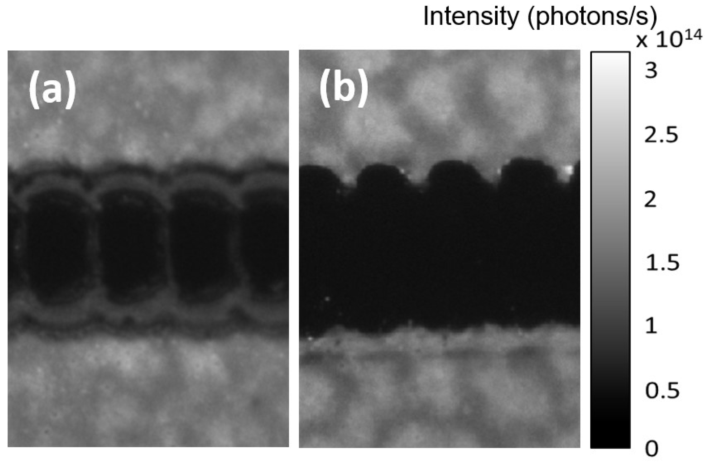
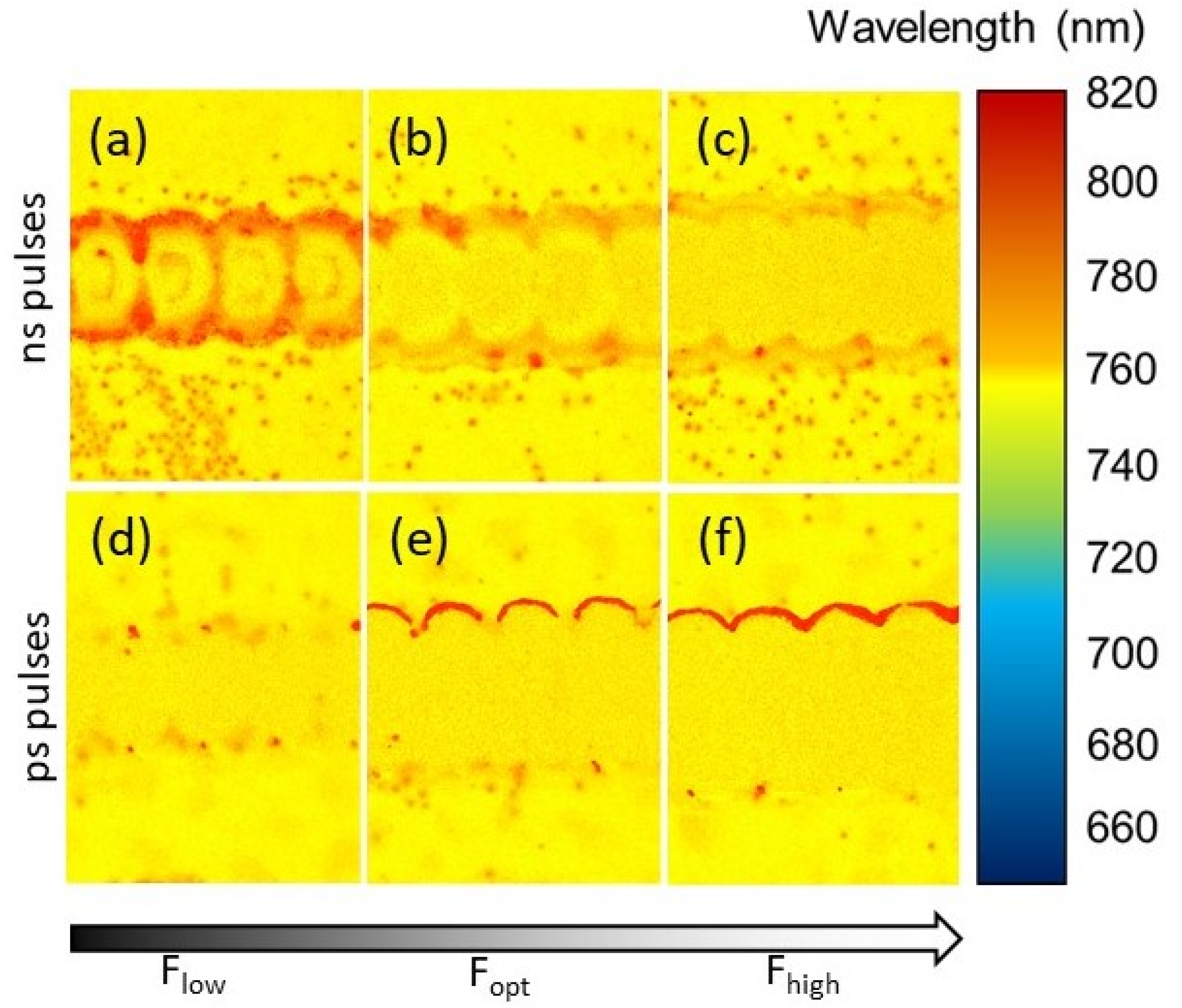
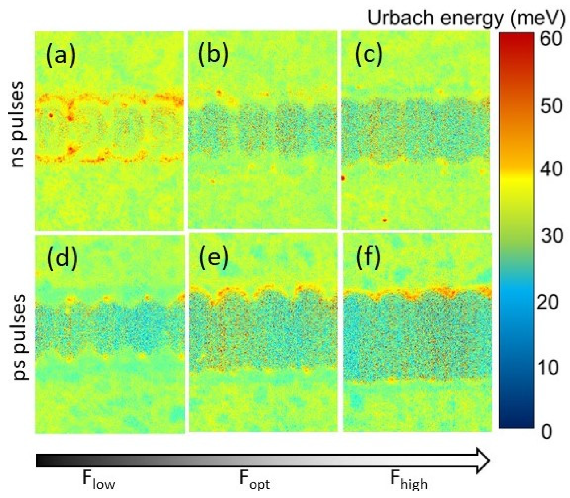
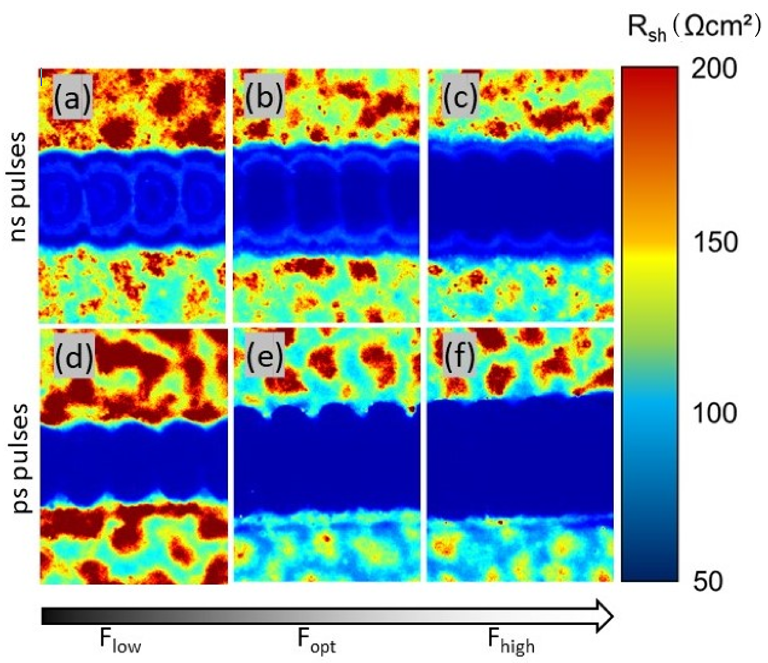
3. Results and Discussion

PL characterization of laser-patterned scribe lines involves acquiring spectrally resolved images of the sample surface. After computational processing (e.g., noise removal), the dataset provides intensity images for each spectral interval, as shown in Figure 1. These images depict the PL intensity for scribe lines created with optimal fluences using ns (Figure 1a) and ps (Figure 1b) laser pulses. Remote areas within the images, considered unaffected by the laser-induced heat, serve as reference points. Perovskite’s thermal diffusion length (~1 µm) aligns with prior findings [12] and reflects the intrinsic material property concerning heat propagation. However, in addition to this, the energy input from the Gaussian pulse flanks induces localized thermal effects beyond the immediate scribe line. Specifically, we observed temperatures of 320 K to 400 K at the edges of the scribe line for ns pulses, leading to the formation of a Br-rich phase at the perovskite/HTL interface adjacent to the scribe. This suggests that the effects of ns laser scribing are not solely confined to the thermal diffusion length but are also influenced by spatial heat flow driven by the dissipated laser energy. This effect was not observed for ps pulses, indicating a distinct difference in the spatial heat flow dynamics between the two pulse regimes.
During raw data processing, the PL intensity was converted into photon flux (photons per second). The photoluminescent flux is presented for a wavelength of 758 nm ± 1 nm, corresponding to the sample’s main PL emission transition. To identify this central wavelength, images were generated displaying the wavelength with the highest PL intensity at each pixel.
Figure 2 displays images of scribe lines patterned with ns (Figure 2a–c) and ps (Figure 2d–f) laser pulses, using varied fluences: too low (Figure 2a,d), optimal (Figure 2b,e), and too high (Figure 2c,f). The images show uniform PL emission with a peak intensity at ~758 ± 3 nm, corresponding to a bandgap energy of ~1.64 eV, which is characteristic of triple-cation PSCs. PL emission was also detected within the scribed trenches, likely from residual absorber material. These residues do not impair the electrical functionality of the series interconnection [9]. Instead, they confirm that the underlying ITO layer remains unaffected during laser patterning, which is crucial for low-loss series interconnections.
Adjacent to the scribe line edges, a pronounced redshift in PL emission is observed, extending up to several tens of nanometers. This shift appears at numerous spots spread across the sample surface, irrespective of the laser pulse duration. At the inner scribe line edges, the redshift is attributed to significant material alterations caused by the patterning process. In contrast, the scattered dots indicate the underlying material removal processes, specifically explosive boiling that occurs immediately after laser irradiation, leading to intense evaporation of the exited volume. Some particles in the evaporation plume condense rapidly, forming splashes widely distributed around the scribe line. This ablation mechanism is consistent with previous studies and supported by simulations [11,29]. Figure 3 shows a statistical analysis of redshifted splashes as a function of fluence and pulse duration, revealing more efficient material removal with ps laser pulses.
The asymmetry in the scribe trench is caused by non-ideality in the Gaussian laser beam profile, resulting in uneven intensity distribution. This leads to one edge of the trench being steeper than the other, which can potentially influence the performance of the P3 interconnection. However, this asymmetry reflects realistic conditions in laser processing and does not necessarily compromise the patterning process. To minimize its impact, the scribing process should be optimized to place the less favorable edge inside the dead area, where it does not affect functionality, while the steeper edge is positioned externally. This ensures that the overall quality of the interconnection is preserved.
With regard to the material removal aspect, ps pulses would be preferable to ns pulses, as condensed debris near the scribe line could increase the surface roughness and make subsequent layer deposition or encapsulation more difficult. However, no damage to the underlying front contact was observed within the tested fluence range.
To access the impact of laser patterning on the perovskite material, the Urbach energy EU serves as a useful parameter. It is directly correlated with trap states in the electronic structure of the perovskite absorber and provides a quantitative measure of the laser effects on material properties. Calculating the Urbach energy begins with determining the central wavelength of the PL emission (see Figure 2). EU provides deeper insights into the density of electronic states near the band edges and serves as an indicator of the local electronic quality of the absorber layer in solar cells [36,37,38,39]. Lower EU values indicate a reduced density of electronic defect states, which in turn results in a higher open-circuit voltage (Voc) and improved solar cell performance. Although the applicability of EU as a universal metric for perovskite solar cells (PSCs) is still under discussion [36,37], empirical data suggest a correlation between EU and the Voc deficit, making it a useful metric for assessing solar cell power conversion efficiency [38,39,40].
Figure 4 presents spatially resolved images of EU as a function of laser fluence and pulse duration. For ns laser pulses (Figure 4 a–c), a larger number of pixels, and consequently a greater area, with higher EU values is observed at lower fluences, likely due to incomplete material ablation leaving altered perovskite within the scribe line. In contrast, for ps laser pulses, the area with higher EU values increases with fluence, which is attributed to the non-Gaussian beam shape causing more damage at the upper edge. Both laser types are suitable for P3 patterning if fluence is precisely optimized. However, from a reliability perspective, ns laser pulses may be preferable, as perovskite material shows less sensitivity to higher fluences until damage to underlying layers occurs.
Shunt resistance is a practical metric for evaluating the electrical performance of solar cells and can be used to assess the quality of laser scribe lines. Following an approach introduced by Augarten et al. [32], shunt resistance can be derived from PL images captured under varying illumination intensities (i.e., different photon fluxes). In this study, we modified the method by Augarten et al., acquiring PL images at a fixed illumination intensity but using different photon energies (405 nm and 532 nm). This requires consideration of the spectral response, determined through measurement of the external quantum efficiency (EQE). Using this adapted method, Figure 5 presents local shunt resistance images as a function of laser pulse duration and fluence, providing insight into the effects of laser scribing on the electrical properties of the sample.
The images of local shunt resistance reveal island-like regions next to the scribe lines with significantly varying shunt resistances. Within the scribe lines, the shunt resistance is uniform, but it increases abruptly at the edges towards distant regions. High fluences lead to less distinct scribe line edges, indicating material changes due to the laser treatment. These island-like structures suggest local material inhomogeneities, likely bromide- and iodide-rich areas, implying material degradation. Shunt resistance analysis shows no significant differences between ns and ps laser pulses. High fluences alter the material, but due to variable shunt resistance in remote areas, the impact of high fluences on scribe line quality remains unclear and requires further investigation.
In order to assess the influence of laser parameters, particularly fluence and pulse length, on the overall electrical properties of the interconnected solar cells and to correlate these findings with the spatially resolved mapping images, j–V curves (current density vs. voltage) were recorded. Figure 6 provides such j–V curves for three-segmented mini-modules, each P3 patterned under different laser fluence regimes: (a) low fluence, (b) optimal fluence, and (c) high fluence. The black curves represent patterning with ns laser pulses, and the blue curves represent patterning with ps laser pulses. The results demonstrate that well-functioning series interconnections of solar cells were achieved across the investigated fluence regimes, confirming the robustness of the laser scribing process. The process tolerates variations in sample composition and layer thickness, making it suitable for variations in the production conditions.
However, the comparison of the j–V curves of the three fluence regimes reveals some systematic variations in the electrical performance. At low fluence, both laser types exhibit poorer performance, likely due to insufficient material removal. Optimal fluence achieves the best results, especially for ns laser pulses, balancing effective scribing with minimal damage. At high fluence, performance losses occur again, likely due to overheating and excessive material removal.
To better understand the differences between the fluence regimes and identify potential losses, the key cell parameters were extracted from the j–V curves and compared. It is important to note that different, though nominally identical, batches were prepared for the three fluence regimes. This may lead to variations in the cell properties despite identical preparation conditions. Thus, we prioritized a meaningful comparison of solar cell parameters that provide insights into electrical losses, in particular the fill factor FF, power conversion efficiency η, series resistance Rs, and shunt resistance Rsh. These parameters were selected because they reflect the electrical interplay among all solar cell components and are less dependent on specific material properties. Derived from the j–V curves, they were chosen for their relevance to our study and their relative independence from batch-to-batch fluctuations, ensuring reliable evaluation of the laser processing effects.
Figure 7 compares these key cell parameters as a function of fluence for ns (left column) and ps (right column). Each parameter is plotted against fluence (J/m2), with dotted lines connecting the data points to indicate trends. In accordance with the curves in Figure 7, FF and η reach their maximum at optimal fluences and decrease at lower and higher fluences, highlighting the balance between minimized losses and effective charge extraction. The investigation of Rs helps determine whether the ITO layer remained intact during the patterning process. The results show that Rs stayed low and relatively stable across all fluences, highlighting the precision and consistency, particularly of ps laser processing. In contrast, Rsh was analyzed to find indications of severe material damage and the related presence of increased densities of defect-related trap states. When comparing the values for the ns and ps at optimal fluences, they appear to be inconsistent with the trends in j–V behavior. However, it should be noted that they are correct, possibly due to differences in the voltage dependence of the shunt losses. Here, the focus is mainly on changes in Rsh with fluence rather than its absolute value. While the maximum for Rsh shows the expected behavior and is reached at the optimal fluence for ps pulses, Rsh generally increases slightly for ns pulses, but without this having a decisive influence on FF and η. This behavior could be due to the thermal nature of the ns pulses, which can lead to material changes, such as the formation of excess PbI2 or the formation of a bromine-rich interlayer, which affects the electrical properties but can still improve the overall photovoltaic performance [12].
In summary, the electrical parameters provide a comprehensive assessment of the module performance, confirming that the scribing process has nearly no negative impact on device functionality at optimal fluence. The inclusion of Rs demonstrates that the underlying contact remains fully functional without laser-induced damage, while efficiency and FF serve as integral measures of the overall module performance. Although the overall electrical performance of the modules is influenced by multiple factors beyond P3, our results demonstrate that hyperspectral PL imaging provides valuable insights into the local material modifications induced by P3 scribing. These modifications, such as changes in Urbach energy and shunt resistance, affect interconnection quality and, consequently, can contribute to variations in electrical performance.
While PL imaging is a powerful tool for analyzing local effects around the scribe lines, such as potential material changes and structural integrity, it primarily reflects localized changes induced by the patterning process. In contrast, the electrical parameters act as global indicators of the functionality of the module, ensuring that the device remains operational with minimal laser-induced damage.

4. Summary and Conclusions

This study investigated the impact of laser pulse duration and fluence on the perovskite layer during P3 patterning for the serial interconnection of perovskite solar cells, as well as its influence on the photovoltaic performance of the interconnected cells. Hyperspectral PL imaging was utilized to visualize the spatial effects of varying pulse durations and fluence, capturing both the patterning lines and surrounding edges. This method allowed us to determine key parameters, such as central PL wavelength, EU, and Rsh, with lateral resolution. These parameters provided insights into the electrical and geometric interconnection losses associated with different pulse durations and fluence regimes.
The analysis demonstrated that successful patterning is achievable with both ps and ns laser pulses, indicating that perovskite shows low sensitivity to laser-induced thermal effects. This conclusion is evidenced by the abrupt changes in EU at the edges of the scribe lines, suggesting minimal influence from laser pulse duration. However, different interaction processes of the laser pulses with the layers to be processed were identified. With ns pulses, low fluences result in insufficient material removal. With ps pulses, high fluences cause blurred edges. Hyperspectral images also revealed small dots resembling splashes around the trenches, particularly in ns-patterned samples, indicating explosive boiling and condensation as the dominant ablation mechanisms.
Additionally, the evaluation identified a redshift in the PL signal and increased shunt resistance, both of which point to material modifications caused by the laser patterning process. The effects of the laser fluence on the electric parameters of the interconnected solar cell are more pronounced than those of pulse duration. However, even with deviations from optimal patterning parameters, satisfactory cell performance was achievable, demonstrating the robustness of the process window to manufacturing fluctuations.
This robustness is a significant advantage for industrial scalability. The findings indicate that the laser patterning process maintains efficacy across a range of fluence values and can compensate for variations in sample composition and film thickness. Consequently, the process is well-suited for large-scale production and adaptable to varying manufacturing conditions.

Author Contributions

Conceptualization, C.S. and B.S.; data curation, C.S., M.F., L.-I.D.-B., G.G., S.M. and J.D.; formal analysis, C.S., N.O., L.-I.D.-B. and B.S.; funding acquisition, C.S. and B.S.; investigation, C.S., M.F., N.O., L.-I.D.-B., G.G., S.M. and J.D.; methodology, C.S. and B.S.; project administration, E.U., R.S. and B.S.; resources, L.-I.D.-B., J.D., E.U., R.S. and B.S.; supervision, E.U., R.S. and B.S.; validation, C.S., N.O., L.-I.D.-B. and B.S.; visualization, C.S. and B.S.; writing—original draft, C.S., M.F. and B.S.; writing—review and editing, C.S., N.O. and B.S. All authors have read and agreed to the published version of the manuscript.

Funding

This research was funded by HTW Berlin, project “LasTa”.

Institutional Review Board Statement

Not applicable.

Informed Consent Statement

Not applicable.

Data Availability Statement

The data that support the findings of this study are available from the corresponding author upon reasonable request.

Acknowledgments

Experimental support from the PVcomB and HZB (EE-IS) teams is acknowledged. We thank S. Siebentritt (University of Luxembourg) for fruitful discussions.

Conflicts of Interest

Authors Laura-Isabelle Dion-Bertrand, Guillaume Gélinas and Stéphane Marcet were employed by Photon etc. The remaining authors declare that the research was conducted in the absence of any commercial or financial relationships that could be construed as a potential conflict of interest.

References

  1. Manser, J.S.; Christians, J.A.; Kamat, P.V. Intriguing optoelectronic properties of metal halide perovskites. Chem. Rev. 2016, 116, 12956–13008. [Google Scholar] [CrossRef] [PubMed]
  2. Kim, G.-W.; Petrozza, A. Defect Tolerance and Intolerance in Metal-Halide Perovskites. Adv. Energy Mater. 2020, 10, 2001959. [Google Scholar] [CrossRef]
  3. Green, M.A.; Dunlop, E.D.; Yoshita, M.; Kopidakis, N.; Bothe, K.; Siefer, G.; Hao, X.; Jiang, J.Y. Solar Cell Efficiency Tables (Version 65). Prog. Photovolt. Res. Appl. 2025, 33, 3–15. [Google Scholar] [CrossRef]
  4. Sheng, Y.; Wen, X.; Jia, B.; Gan, Z. Direct laser writing on halide perovskites: From mechanisms to applications. Light Adv. Manuf. 2024, 4, 95–116. [Google Scholar] [CrossRef]
  5. Zhou, C.; Cao, G.; Gan, Z.; Ou, Q.; Chen, W.; Bao, Q.; Jia, B.; Wen, X. Spatially Modulating the Fluorescence Color of Mixed-Halide Perovskite Nanoplatelets through Direct Femtosecond Laser Writing. ACS Appl. Mater. Interfaces 2019, 11, 26017–26023. [Google Scholar] [CrossRef]
  6. Zhang, Y.; Lin, Y.; Lin, Z.; Yan, Z.; Shuli, W.; Su, Y.; Lin, Y.; Kuo, H.C.; Chen, Z.; Lai, S.; et al. Application of Ultrafast Lasers: A Promising Route toward the Fabrication of Advanced Perovskite-Based Devices. Adv. Opt. Mater. 2025, 13, 2402924. [Google Scholar] [CrossRef]
  7. Yan, G.; Yuan, Y.; Kaba, M.; Kirchartz, T. Visualizing Performances Losses of Perovskite Solar Cells and Modules: From Laboratory to Industrial Scales. Adv. Energy Mater. 2024, 15, 2403706. [Google Scholar] [CrossRef]
  8. Stegemann, B.; Schultz, C. Laser patterning of thin films. In Digital Encyclopedia of Applied Physics; Wiley-VCH Verlag GmbH & Co. KGaA: Hoboken, NJ, USA, 2019; pp. 1–30. [Google Scholar] [CrossRef]
  9. Matteocci, F.; Vesce, L.; Kosasih, F.U.; Castriotta, L.A.; Cacovich, S.; Palma, A.L.; Divitini, G.; Ducati, C.; Di Carlo, A. Fabrication and Morphological Characterization of High-Efficiency Blade-Coated Perovskite Solar Modules. ACS Appl. Mater. Interfaces 2019, 11, 25195–25204. [Google Scholar] [CrossRef]
  10. Mincuzzi, G.; Palma, A.L.; Di Carlo, A.; Brown, T.M. Laser Processing in the Manufacture of Dye-Sensitized and Perovskite Solar Cell Technologies. ChemElectroChem 2016, 3, 9–30. [Google Scholar] [CrossRef]
  11. Schultz, C.; Fenske, M.; Dagar, J.; Zeiser, A.; Bartelt, A.; Schlatmann, R.; Unger, E.L.; Stegemann, B. Ablation mechanisms of nanosecond and picosecond laser scribing for metal halide perovskite module interconnection—An experimental and numerical analysis. Sol. Energy 2020, 198, 410–418. [Google Scholar] [CrossRef]
  12. Fenske, M.; Schultz, C.; Dagar, J.; Kosasih, F.U.; Zeiser, A.; Junghans, C.; Bartelt, A.; Ducati, C.; Schlatmann, R.; Unger, E.; et al. Improved Electrical Performance of Perovskite Photovoltaic Mini-Modules through Controlled PbI2 Formation Using Nanosecond Laser Pulses for P3 Patterning. Energy Technol. 2021, 9, 2000969. [Google Scholar] [CrossRef]
  13. Schultz, C.; Fenske, M.; Dion-Bertrand, L.-I.; Gélinas, G.; Marcet, S.; Dagar, J.; Bartelt, A.; Schlatmann, R.; Unger, E.; Stegemann, B. Hyperspectral Photoluminescence Imaging for Spatially Resolved Determination of Electrical Parameters of Laser-Patterned Perovskite Solar Cells. Sol. RRL 2023, 7, 2300538. [Google Scholar] [CrossRef]
  14. Trupke, T.; Bardos, R.A.; Abbott, M.D.; Cotter, J.E. Suns-photoluminescence: Contactless determination of current-voltage characteristics of silicon wafers. Appl. Phys. Lett. 2005, 87, 093503. [Google Scholar] [CrossRef]
  15. Abou-Ras, D.; Kirchartz, T.; Rau, U. Photoluminescence Analysis of Thin-Film Solar Cells; Abou-Ras, D., Kirchartz, T., Rau, U., Eds.; WILEY-VCH Verlag GmbH & Co. KGaA: Hoboken, NJ, USA, 2016; pp. 275–297. [Google Scholar] [CrossRef]
  16. Siebentritt, S.; Weiss, T.P.; Sood, M.; Wolter, M.H.; Lomuscio, A.; Ramirez, O. How photoluminescence can predict the efficiency of solar cells. J. Phys. Mater. 2021, 4, 042010. [Google Scholar] [CrossRef]
  17. Kirchartz, T.; Márquez, J.A.; Stolterfoht, M.; Unold, T. Photoluminescence-Based Characterization of Halide Perovskites for Photovoltaics. Adv. Energy Mater. 2020, 10, 1904134. [Google Scholar] [CrossRef]
  18. Schubert, M.C.; Mundt, L.E.; Walter, D.; Fell, A.; Glunz, S.W. Spatially Resolved Performance Analysis for Perovskite Solar Cells. Adv. Energy Mater. 2020, 10, 1904001. [Google Scholar] [CrossRef]
  19. Delamarre, A.; Paire, M.; Guillemoles, J.-F.; Lombez, L. Quantitative luminescence mapping of Cu(In,Ga)Se2 thin-film solar cells. Prog. Photovolt. Res. Appl. 2015, 23, 1305–1312. [Google Scholar] [CrossRef]
  20. Nguyen, K.; Bui, A.D.; Mayon, A.O.; Nguyen, T.; White, T.; Truong, T.; Ho-Baillie, A.; Duong, T.; Shen, H.; Weber, K.; et al. Correlative imaging of optoelectronic properties for perovskite solar cells via hyperspectral luminescence imaging. Cell Rep. Phys. Sci. 2023, 4, 13. [Google Scholar] [CrossRef]
  21. Delamarre, A.; Lombez, L.; Guillemoles, J.-F. Characterization of solar cells using electroluminescence and photoluminescence hyperspectral images. J. Photonics Energy 2012, 2, 027004. [Google Scholar] [CrossRef]
  22. Levtchenko, A.; Lopez-Varo, P.; Provost, M.; Medjoubi, K.; Rousset, J.; Ory, D. Perovskite Mini-Module Voltage Loss Quantification and Analysis by Large-Scale Hyperspectral Photoluminescence Imaging. Sol. RRL 2025, 9, 2400796. [Google Scholar] [CrossRef]
  23. El-Hajje, G.; Momblona, C.; Gil-Escrig, L.; Ávila, J.; Guillemot, T.; Guillemoles, J.-F.; Sessolo, M.; Bolink, H.J.; Lombez, L. Quantification of spatial inhomogeneity in perovskite solar cells by hyperspectral luminescence imaging. Energy Environ. Sci. 2016, 9, 2286–2294. [Google Scholar] [CrossRef]
  24. Rey, G.; Paduthol, A.; Sun, K.; Nagle, T.; Poplavskyy, D.; Serrano Escalante, V.; Melchiorre, M.; Siebentritt, S.; Abbott, M.; Trupke, T. Photoluminescence-Based Method for Imaging Buffer Layer Thickness in CIGS Solar Cells. IEEE J. Photovolt. 2020, 10, 181–187. [Google Scholar] [CrossRef]
  25. Bui, A.D.; Nguyen, D.-T.; Fell, A.; Mozaffari, N.; Ahmad, V.; Duong, T.; Li, L.; Truong, T.N.; Wibowo, A.A.; Nguyen, K.; et al. Spatially resolved power conversion efficiency for perovskite solar cells via bias-dependent photoluminescence imaging. Cell Rep. Phys. Sci. 2023, 4, 101641. [Google Scholar] [CrossRef]
  26. Hameiri, Z.; Mahboubi Soufiani, A.; Juhl, M.; Liangcong, J.; Huang, F.; Bing, C.; Kampwerth, H.; Weber, J.; Green, M.; Trupke, T. Photoluminescence and electroluminescence imaging of perovskite solar cells. Prog. Photovolt. Res. Appl. 2015, 23, 1697–1705. [Google Scholar] [CrossRef]
  27. Hacene, B.; Laufer, F.; Ternes, S.; Farag, A.; Pappenberger, R.; Fassl, P.; Moghadamzadeh, S.; Nejand, B.A.; Feeney, T.; Howard, I.; et al. Intensity Dependent Photoluminescence Imaging for In-Line Quality Control of Perovskite Thin Film Processing. Adv. Mater. Technol. 2024, 9, 2301279. [Google Scholar] [CrossRef]
  28. Zikulnig, J.; Mühleisen, W.; Bolt, P.J.; Simor, M.; De Biasio, M. Photoluminescence Imaging for the In-Line Quality Control of Thin-Film Solar Cells. Solar 2022, 2, 1–11. [Google Scholar] [CrossRef]
  29. Schultz, C.; Fenske, M.; Dagar, J.; Farias Basulto, G.A.; Zeiser, A.; Bartelt, A.; Junghans, C.; Schlatmann, R.; Unger, E.; Stegemann, B. Laser-based series interconnection of chalcopyrite und perovskite solar cells: Analysis of material modifications and implications for achieving small dead area widths. Mater. Today Proc. 2022, 53, 299–306. [Google Scholar] [CrossRef]
  30. Cacovich, S.; Vidon, G.; Degani, M.; Legrand, M.; Gouda, L.; Puel, J.-B.; Vaynzof, Y.; Guillemoles, J.-F.; Ory, D.; Grancini, G. Imaging and quantifying non-radiative losses at 23% efficient inverted perovskite solar cells interfaces. Nat. Commun. 2022, 13, 2868. [Google Scholar] [CrossRef]
  31. Wolter, M.H.; Carron, R.; Avancini, E.; Bissig, B.; Weiss, T.P.; Nishiwaki, S.; Feurer, T.; Buecheler, S.; Jackson, P.; Witte, W.; et al. How band tail recombination influences the open-circuit voltage of solar cells. Prog. Photovolt. Res. Appl. 2022, 30, 702–712. [Google Scholar] [CrossRef]
  32. Augarten, Y.; Trupke, T.; Lenio, M.; Bauer, J.; Weber, J.W.; Juhl, M.; Kasemann, M.; Breitenstein, O. Calculation of quantitative shunt values using photoluminescence imaging. Prog. Photovolt. Res. Appl. 2013, 21, 933–941. [Google Scholar] [CrossRef]
  33. El-Hajje, G.; Ory, D.; Paire, M.; Guillemoles, J.F.; Lombez, L. Contactless characterization of metastable defects in Cu(In,Ga)Se2 solar cells using time-resolved photoluminescence. Sol. Energy Mater. Sol. Cells 2016, 145, 462–467. [Google Scholar] [CrossRef]
  34. Ramírez Quiroz, C.O.; Dion-Bertrand, L.-I.; Brabec, C.J.; Müller, J.; Orgassa, K. Deciphering the Origins of P1-Induced Power Losses in Cu(Inx,Ga1–x)Se2 (CIGS) Modules Through Hyperspectral Luminescence. Engineering 2020, 6, 1395–1402. [Google Scholar] [CrossRef]
  35. Delamarre, A.; Lombez, L.; Guillemoles, J.-F. Contactless mapping of saturation currents of solar cells by photoluminescence. Appl. Phys. Lett. 2012, 100, 131108. [Google Scholar] [CrossRef]
  36. Kaiser, C.; Sandberg, O.J.; Zarrabi, N.; Li, W.; Meredith, P.; Armin, A. A universal Urbach rule for disordered organic semiconductors. Nat. Commun. 2021, 12, 3988. [Google Scholar] [CrossRef]
  37. Holovský, J.; Ridzoňová, K.; Peter Amalathas, A.; Conrad, B.; Sharma, R.K.; Chin, X.Y.; Bastola, E.; Bhandari, K.; Ellingson, R.J.; De Wolf, S. Below the Urbach Edge: Solar Cell Loss Analysis Based on Full External Quantum Efficiency Spectra. ACS Energy Lett. 2023, 8, 3221–3227. [Google Scholar] [CrossRef]
  38. Chantana, J.; Kawano, Y.; Nishimura, T.; Mavlonov, A.; Minemoto, T. Impact of Urbach energy on open-circuit voltage deficit of thin-film solar cells. Sol. Energy Mater. Sol. Cells 2020, 210, 110502. [Google Scholar] [CrossRef]
  39. Ugur, E.; Ledinský, M.; Allen, T.G.; Holovský, J.; Vlk, A.; De Wolf, S. Life on the Urbach Edge. J. Phys. Chem. Lett. 2022, 13, 7702–7711. [Google Scholar] [CrossRef]
  40. Ledinsky, M.; Schönfeldová, T.; Holovský, J.; Aydin, E.; Hájková, Z.; Landová, L.; Neyková, N.; Fejfar, A.; De Wolf, S. Temperature Dependence of the Urbach Energy in Lead Iodide Perovskites. J. Phys. Chem. Lett. 2019, 10, 1368–1373. [Google Scholar] [CrossRef]
Figure 1. PL flux (photons per second) images of perovskite samples patterned with (a) ns and (b) ps laser pulses at optimal fluences of 1.36 J/cm2 and 2.31 J/cm2, respectively, showing emission at 758 nm. Size of both images: 101 µm × 133 µm.
Solar 05 00013 g001
Figure 2. Spatially resolved images of the local central PL emission wavelength for samples patterned with (ac) ns and (df) ps laser pulses at three fluence regimes: (a,d) low, (b,e) optimal, and (c,f) high.
Solar 05 00013 g002
Figure 3. Comparison of the number of splashes observed along the laser scribe line for ns and ps laser pulses as a function of the applied fluence. The width of the analyzed area adjacent to the trenches matches the respective trench width.
Solar 05 00013 g003
Figure 4. Spatially resolved images of the local Urbach energy for samples patterned with (ac) ns and (df) ps laser pulses at three fluence regimes: (a,d) low, (b,e) optimal, and (c,f) high.
Solar 05 00013 g004
Figure 5. Spatially resolved images of the local shunt resistance for samples patterned with (ac) ns and (df) ps laser pulses at three fluence regimes: (a,d) low, (b,e) optimal, and (c,f) high.
Solar 05 00013 g005
Figure 6. j–V curves of three-segmented mini-modules patterned with ns and ps laser pulses. The curves are shown for the different fluence regimes: (a) low fluence, (b) optimal fluence, and (c) high fluence, illustrating the impact of laser pulse duration and fluence on the electrical performance of the modules.
Solar 05 00013 g006
Figure 7. Variation of fill factor (FF), power conversion efficiency (η), series resistance (Rs), and shunt resistance (Rsh) as a function of fluence for perovskite samples patterned with (a) ns laser pulses and (b) ps laser pulses. Data points are shown for three fluence regimes (low, optimal, and high).
Solar 05 00013 g007
Table 1. Laser process parameters for sample preparation.
ps Laser
Patterning
ns Laser
Patterning
Wavelength 532 nm
Scribing velocity 500 mm/s
Pulse repetition rate 20 kHz
Pulse duration 10 ps20 ns
Beam diameter 26.7 (±10%) µm28.1 (±10%) µm
Fluences
- OptimalFopt2.31 J/m21.36 J/m2
- Low (ca. half of the optimal value)Flow1.08 J/m20.72 J/m2
- High (ca. twice the optimal value)Fhigh4.31 J/m22.64 J/m2
Disclaimer/Publisher’s Note: The statements, opinions and data contained in all publications are solely those of the individual author(s) and contributor(s) and not of MDPI and/or the editor(s). MDPI and/or the editor(s) disclaim responsibility for any injury to people or property resulting from any ideas, methods, instructions or products referred to in the content.

