Entry

Nanoimprint—Mo(o)re than Lithography

Laboratory for Nano and Quantum Technologies, Paul Scherrer Institute, 5232 Villigen PSI, Switzerland
Encyclopedia 2025, 5(4), 197; https://doi.org/10.3390/encyclopedia5040197
Submission received: 24 July 2025 / Revised: 8 October 2025 / Accepted: 27 October 2025 / Published: 21 November 2025
(This article belongs to the Collection Encyclopedia of Engineering)

Definition

Nanoimprint lithography (NIL) is a high-resolution parallel patterning method based on molding. It has proven resolution down to the nanometer range and can be scaled up for large areas and high throughput. Its main characteristic is that the surface pattern of a mold is imprinted on a material that is displaced locally by using the difference in hardness of the mold and the moldable material, thus replicating its surface topography. This can be achieved by shaping a thermoplastic film by heating and cooling (T-NIL) or a photosensitive resin followed by a curing process for hardening (UV-NIL). In lithography, the local thickness contrast of the thin molded film can be used as a masking layer to transfer the pattern onto the underlying substrate. Therefore, NIL will be an alternative in fields in which electron-beam lithography and photolithography do not provide sufficient resolution at reasonable throughput. Direct imprint enables applications where a modified functional surface is needed without pattern transfer. NIL is currently used for high-volume manufacturing in different applications, like patterned sapphire substrates, wire grid polarizers, photonic devices, lightguides for AR/VR devices, metalenses, and biosensors for DNA analysis, and is being tested for semiconductor integrated circuit chips.

Graphical Abstract

1. Introduction

For current and future devices with functional nanostructured surfaces, high-resolution parallel patterning methods that offer cost-effective manufacturing are required. Nanoimprint lithography (NIL) is the most prominent of the new lithographic techniques. NIL imprints a template with a three-dimensional (3D) surface topography on a moldable material. This is achieved by direct mechanical contact and material displacement. It is different from electron- or photon-based lithography (PL) and therefore incurs no structural loss due to the (optical) proximity effect [1,2]. Yet NIL is similar enough to standard lithography to permit the use of the same manufacturing and technology base: it uses templates made by advanced lithography and silicon process technology, a thin polymer resist as a masking layer for pattern transfer into the underlying substrate by etching (subtractive patterning) or onto it by electroplating (additive patterning), and imprint tools which still have significant resemblance to mask aligners, photolithographic steppers, and anodic bonding tools. NIL is mostly related to lithography. Apart from this, process solutions which are more related to other kinds of shaping processes arise, for example, using the difference in hardness of a mold and a moldable material, such as thermal injection molding (TIM), roll-to-roll (R2R) processes, coining, and casting, with the aim to replicate a mold relief into the surface. The aim of this entry is to present NIL as a basic lithographical process being able to replace standard PL, where a resist layer is patterned by mechanical means instead of exposure and wet development, but also to show that functional materials (e.g., photo- or bio-active materials) can be directly patterned, leading to enhanced functionality of a surface. The chapters on NIL in Springer Handbook of Nanotechnology [3,4] give a good overview about the process chains needed for understanding. The development of NIL towards high-volume manufacturing (HVM), with a variety of references on state-of-the-art techniques and companies, can be found in the book CRC Microlithography—Science and Technology [5]. Newest developments are presented at the annual International Nanoimprint and Nanoprint Technology (NNT) conference, which, in 2025, is celebrating the 30th anniversary since the publication of the first paper by Stephen Chou’s group [6]. This entry is intended to provide basic information about the NIL process and its origins, relate to other processes, and give definitions that make it possible to distinguish process variants, without going into detail about processing issues and specific parameters that might vary.
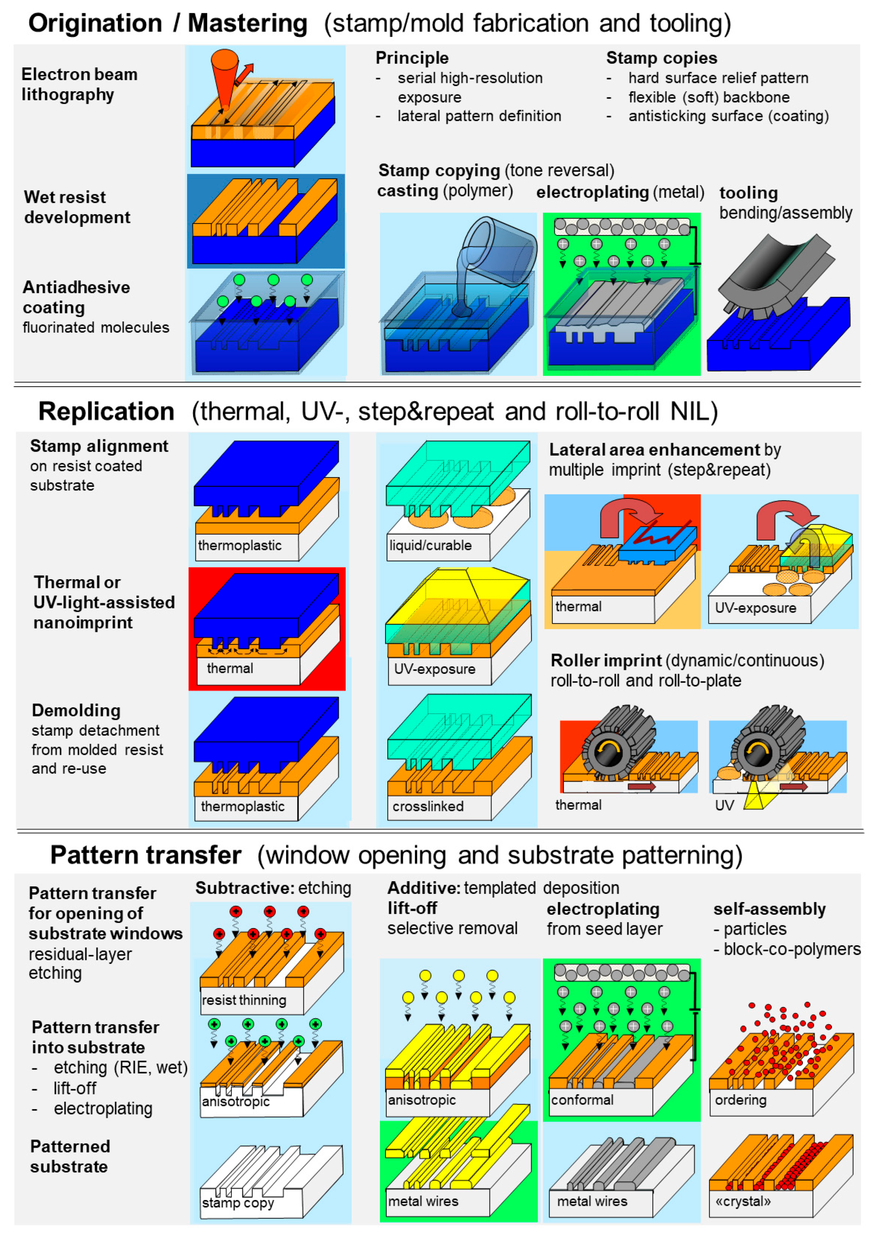
The historical start of NIL was at a time when the surface patterning of silicon wafers was performed using lithography with micrometer resolution. A molding-based lithography process using pattern transfer was demonstrated in the 1970s by Susumu Fujimori at NTT (Tokio, Japan, https://www.global.ntt/ (accessed on 7 July 2025)) in Japan [7], but it was not until 1995, when Stephen Chou and co-workers at the University of Minnesota, USA (later at Princeton University), published their first results, that it started to gain broader attention. They presented NIL as a new type of lithography by demonstrating 10 nm imprint capabilities at a time when 50 nm was considered the PL resolution limit [8,9]. At the same time, NIL, in its variant with UV-curable resists, was developed by Jan Haisma at Philips in Eindhoven, Netherlands [10]. In 2003 NIL was named one of the “10 emerging technologies that will change the world” [11]. NIL was considered revolutionary—and still is, due to three important distinctive characteristics (see Figure 1):
  • It has a proven lateral resolution below 1 nm, which is far ahead of other, photon-based patterning techniques [12,13].
  • It imprints extremely thin polymer films, which result in residual layers of a few nm thickness and can be removed by anisotropic reactive ion etching [1].
  • It can imprint within micro-seconds and replicates multi-level and continuous structures in a variety of functional materials [14,15,16].
NIL is, therefore, considered both disruptive and evolutionary. It is disruptive because it uses the conformal contact of a stamp with a resist layer and displaces the material by squeeze flow and capillary action [11,12,13]. It, therefore, breaks the paradigm of non-contact in modern semiconductor integrated circuit (IC) chip HVM, which was possible by projecting photons and electrons onto a sensitive polymer film by optical means (e.g., lenses, mirrors, and shadow masks) and chemically modifying its solubility. At the same time NIL is evolutionary, because NIL profits from a variety of other technologies for low-cost applications, from large polymer films for packaging to optical versatile devices (OVDs) such as counterfeit tags for security, as well as for Compact Disc molding and micromanufacturing processes used in the so-called LiGA technique (German acronym for lithography, electroforming, and molding) [17,18,19,20]. In a historical context, it is a successor of the book-printing technique by Johannes Gutenberg, who, more than 550 years ago, made significant technological advances by inventing movable metallic letter types that could be copied by metal casting, employing wine presses as printing tools and inks that lasted for centuries. At the same time, it provided an unexpected and untypical solution for Gordon Moore’s law, which, since 1965, predicts the continuous demand for chips with a higher number of transistors and, today, is the driver of innovation in lithography. NIL came at a time when “nano” became the new paradigm of research.

2. Technology

2.1. NIL as a Toolbox for the High-Volume Manufacturing of Nanostructures

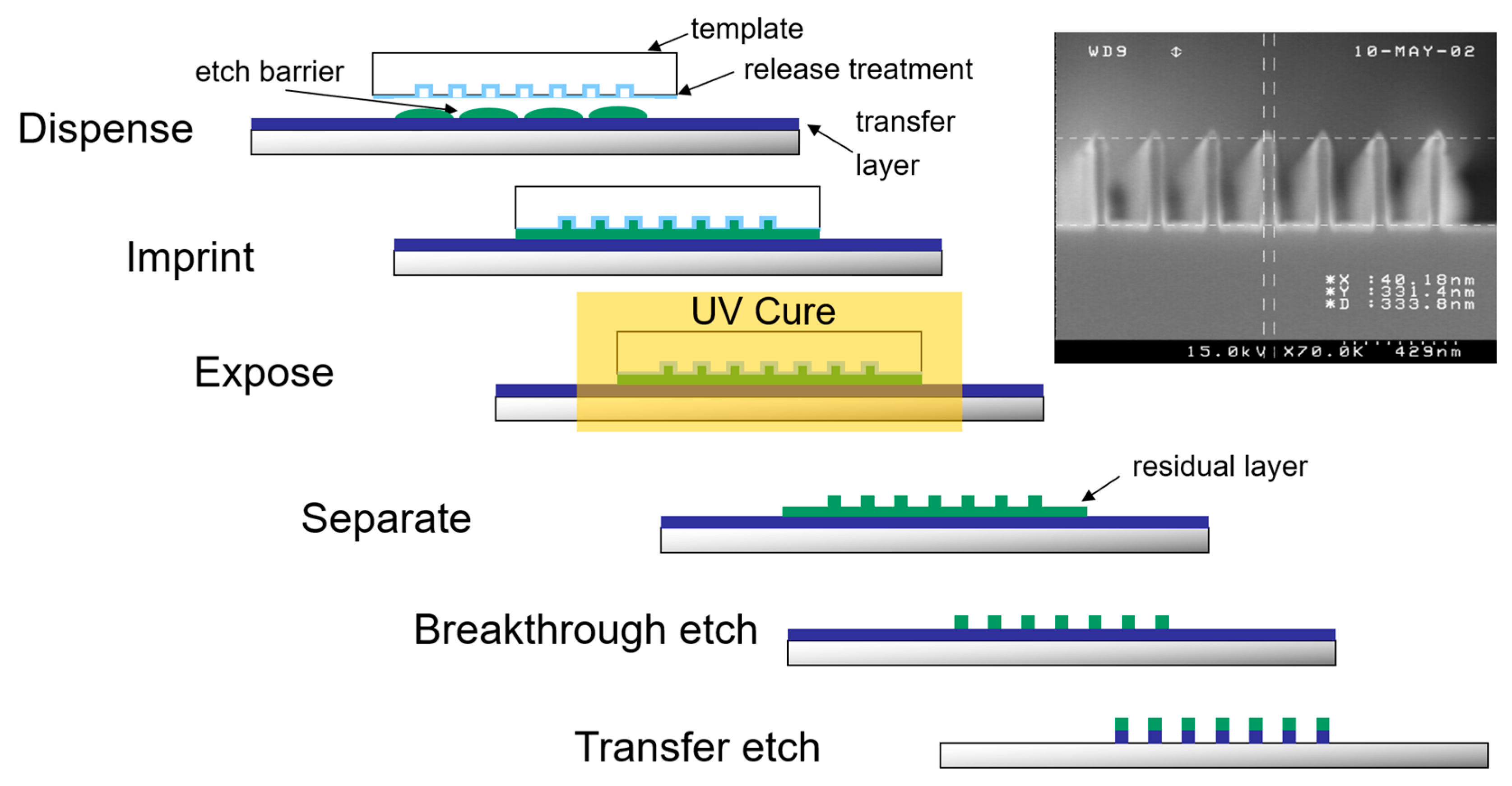
The NIL process is described by the main process steps of imprint, demolding and residual-layer etching [1,2,3,4,21]. Because all structures are patterned at the same time, it is called “parallel”, in contrast to a “serial” direct writing process like electron-beam lithography (EBL). The result is patterned film which conforms to the original surface topography of the stamp but which has to be, according to its purpose, extremely thin with high thickness contrast between the areas in which the stamp protrusions were pressing into the material and the cavities which were filled by the displaced material. The three main NIL process steps can be characterized as follows (see schematics in Figure 2):
  • The imprint, mold filling, or replication process is performed by pressing a stamp with a surface topography onto a material which undergoes displacement by squeeze flow (lateral flow-induced “push” due to the pressing of stamp protrusions into viscous material) or by capillary action (“pull” of material due to wetting and balance of surface energy) and can be molded. If the material is not liquid in its initial state, it must be made viscous. The air in the cavities of the stamp is either removed before molding, displaced to the side, or dissolved in the polymer.
  • Demolding (de-embossing) is the detachment of the mold from the molded material. For this the material must become mechanically robust (solid) so that the surface topography is preserved during the following process steps. Given the mold’s primarily vertical sidewalls, demolding is based on overcoming the adhesion of the stamp surfaces to the polymer and a vertical sliding movement. Often, peeling effects can be exploited because stamps are often bendable and able to delaminate. Thus, during a dynamic process, the stamp is locally separated from the molded structures, enabling air to come in from the sides during demolding. Typically, the condition for NIL is that only vertical or positive slopes are allowed, enabling the demolding of fully hardened materials without undercuts (the so-called demolding constraint). If the stamp structures are flexible enough to allow demolding without damage (distortion or cohesive failure) or can be removed by dissolution, any kind of stamp geometry, e.g., grating ridges with slanted sidewalls and freeform surface topographies, can be demolded.
  • Residual-layer etching is the homogeneous resist thinning that is required for window opening, i.e., the removal of polymer in the depressed areas of the resist before it can be used as a resist for pattern transfer, i.e., the conversion of the resist topography into a different material, by additive or subtractive transfer into or onto the underlying substrate. Since this is often achieved by anisotropic dry etching (sputtering) using oxygen plasma, it is often called breakthrough etching. In semiconductor processing, where very thin layers are used, it is also called descum process, used for the removal of resist residues.
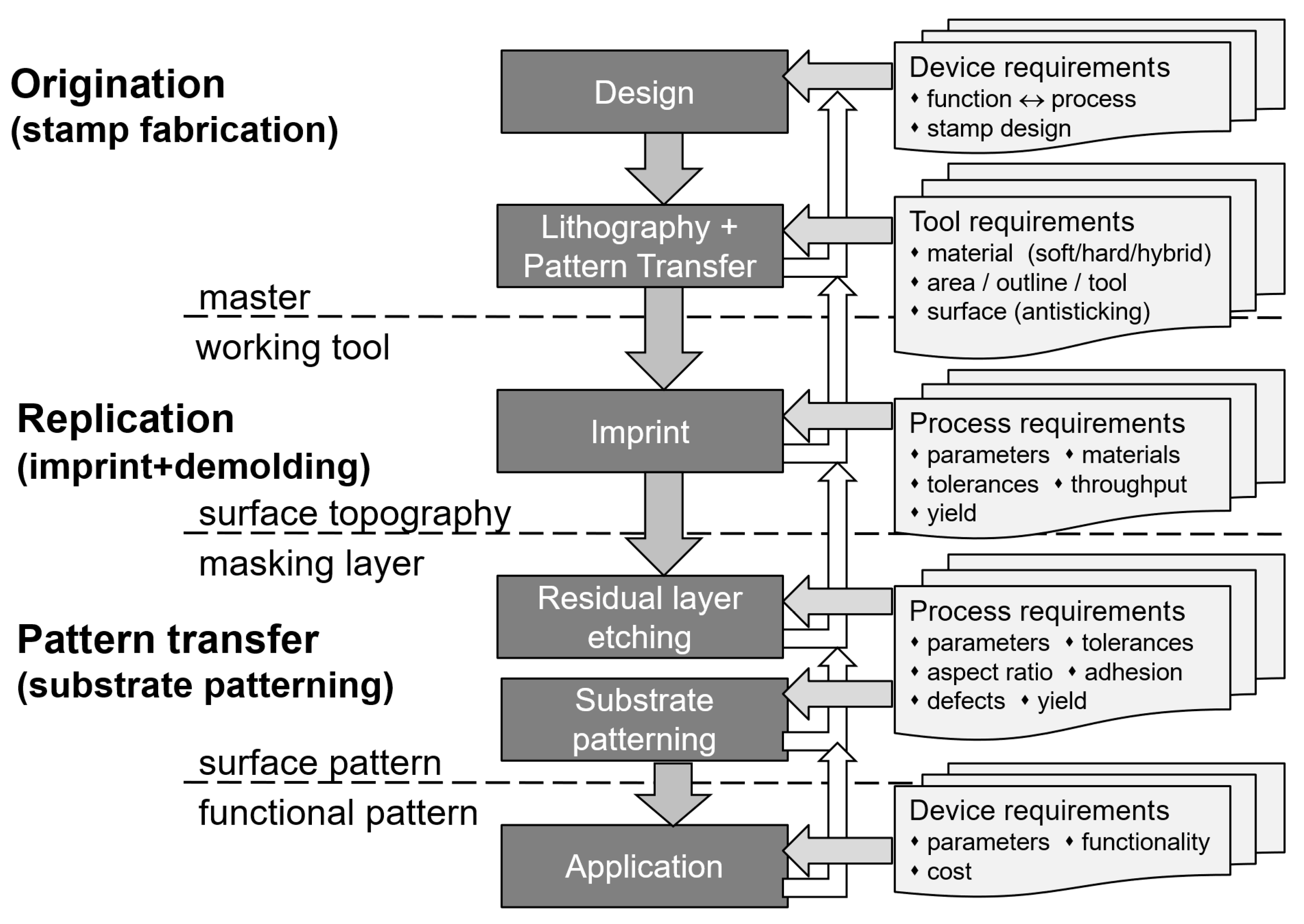
The processes needed to fabricate stamps (origination or mastering) and perform these pattern transfer processes are like standard micro- and nano-lithographic processes. Therefore, strictly speaking, NIL is considered “lithography” only if a pattern transfer step is performed following imprint and demolding. This is a conversion of the polymer layer into a different material by additive or subtractive transfer, and the resist is considered a sacrificial layer that is removed after the process (see Figure 3). In a general view, however, NIL is understood as a variety of processes; therefore, imprint on a functional polymer layer is often also called NIL. For simplicity and comparison with PL, residual-layer etching is considered an integral part of the imprint and demolding sequence and not of pattern transfer, since it does not involve any material conversion.

2.2. Thermal NIL and UV-Assisted NIL

From the beginning, two major variants of NIL have been developed: heat-assisted NIL (thermal or T-NIL) and UV-assisted NIL (UV-NIL). T-NIL is closer to hot embossing (mainly used for microstructuring) [20] and UV-NIL to PL [22,23,24]:
  • In thermal imprint lithography (T-NIL), a stamp is pressed into thin thermoplastic film which is made viscous by heating; after the film conforms to the topography of the stamp, the film is cooled down until it is solid, and the stamp is detached. The main characteristic of such thermoplastic film is its glass transition temperature Tg, above which the film is transformed into the visco-elastic and then viscous state; thus, the thermomechanical properties of a film can be varied by heating and cooling. Typically, temperatures higher than Tg enable faster molding at lower viscosity, but since the entire stack of stamp, film, and substrate must often be heated and cooled within a thermocycle between the molding and demolding states, a large overhead must be considered. Viscosity is in the range of 103 to 107 Pa·s, and the filling of mold cavities can often be described by squeeze flow. A typical thermoplastic polymer is poly(methyl methacrylate) (PMMA), with a Tg of 100–120 °C, which can be imprinted at a temperature of 160–180 °C and demolded at 40–60 °C. Commercial polymers have been developed with better suitability for pattern transfer (higher etch resistance to reactive ion etching). They are typically solvent-based and can be spin-coated before patterning.
  • UV imprint lithography (UV-NIL) uses a liquid pre-polymer with low viscosity which includes a photo initiator and a crosslinking agent. After filling, the material is chemically altered by exposing it, in most cases through the stamp, which, due to crosslinking, like negative photoresists, becomes insoluble. After hardening, the stamp can be detached and the structures demolded. Since viscosity is often in the range of 10−3 to 10−2 Pa·s, capillary filling is responsible for stamp filling, which allows for room-temperature molding at moderate pressure. Both spin-coating and ink-jetting are used to form the desired resist film (typically pre-polymers with solvent).
Both processes are easily scalable if stamps that have the same size as the substrate can be provided. There are a variety of thermoplastic polymers for T-NIL, including functional polymers which can be used directly after being patterned. A silicon wafer can be used as an opaque stamp, as it can be patterned using standard lithographic processes and has an adapted thermal expansion with respect to a silicon substrate. Metal, e.g., nickel, which can be electroplated from resist masters, is rarely used because of its huge thermal expansion mismatch with respect to silicon. In contrast to this, UV-NIL requires transparent stamps, for which fused silica and transparent polymers are used. Due to its compatibility with PL, UV-NIL is currently favored by many enterprises for HVM. As stamps, a variety of materials from fused silica to elastomeric materials like poly(dimethyl siloxane (PDMS) are used, as well as composite stamps using hard PDMS, sol–gel, or epoxy on top of a flexible, soft backbone (soft PDMS) or poly(ethylene terephthalate) (PET)), all achieving sub-50 nm resolution (see Section 2.3) [25]. Room-temperature NIL is clearly an asset reducing cycle times and thermal impact on overlay and precision, and resolution is similar to that achieved with T-NIL. Other processes, such as pulsed NIL, also enable fast T-NIL but require stamps with integrated direct resistive heating at the surface, enabling a short rise in temperature to above 300 °C without significant degradation of the resist [15]. For high-end applications requiring the overlay of different lithographic steps down to below 5 nm, thermal expansion and mechanical deformation must be controlled over large areas.

2.3. Hard and Soft Stamps

Stamps are the intermediate tools that are in mechanical contact with the resist, exert pressure, and enable lateral flow from stamp protrusions to cavities and vertical flow into the cavities. They contain the “binary information” of the resist structures as topographical contrast, defined by feature sizes and locations, both in close vicinity and over long distances. Since they resemble the masks in PL, they are often called masks, dies, or templates. In PL, optical proximity correction and double or even quadruple patterning transforms the required design into a mask absorber pattern that only after projection and wet development reveals its definite form. Different from PL masks, for a 1X contact stamp, the local structure is basically the inverted topography of the stamp surface; i.e., recessed areas in the stamp will become the resist patterns masking the substrate, and stamp protrusion will become the trenches in the resist pattern where the substrate windows are opened. Therefore, no proximity effect must be compensated for. In contrast to this, for some applications, auxiliary cavities may help to compensate for huge density variation, equilibrate inhomogeneities in residual-layer thickness, reduce long distances for squeeze flow, or stabilize structures that might be mechanically weak. Stamp hardness and flexibility are essential to achieving high resolution but also to enable the patterning of non-planar substrates with surface undulations over large and small distances and print over defects:
  • Hard stamps exhibit the highest resolution and have long lifetime and low defectivity. They are made from silicon, fused silica (SiO2), metal, or diamond-like carbon. However, they are also prone to damage if imprinted on particles (e.g., ceramic particles released from mechanical elements due to mechanical friction and wear) which cannot be deformed, since they are often harder than the stamp material. Hard stamps are used for T-NIL because of the high pressure. For JFIL, high stiffness is required for overlay of a few nm. Even hard stamps, with their limited flexibility, can bend slightly to push out air and demolding by delamination [26].
  • Soft stamps enable conformal contact to surface undulations and topographies at low pressure. They are often made from polymers or composed of different layers, e.g., by molding elastomeric or thermoplastic materials. This involves copying from hard masters. Resolution is dependent on the mechanical properties and can be tuned. Often a trade-off must be found, and hybrid solutions (high stiffness at the stamp protrusions and soft backbone) need to be employed. Because of its wide use, also in microcontact printing (µCP), processes using soft stamps are called “soft lithography” [27,28]. Today, most tool manufacturers use flexible stamps, with a hard structured surface layer and a flexible backbone. For specific NIL processes, such as substrate conformal imprint lithography (SCIL), inflatable molds which enable subsequent patterning from one side of an extended substrate to the other while squeezing out the air to one side have been developed. In addition, the demolding is performed by retracting the stamp continuously or stepwise from the substrate by peeling [29].
Today, all applications heading for HVM employ stamp copying, i.e., the multiplication of stamps by NIL, which are needed for backup of valuable master stamps or simply as replacement after a certain threshold of wear and accumulation of defects has been reached [2,30,31]. Some companies even use a new stamp copy for each individual imprint, enabling the removal of particle contamination within the stamp by incorporation. Due to the large surface of a stamp with the imprinted material and the need to remove the stamp from the molded polymer surface without damage, the surface of the stamp must exhibit antisticking behavior to enable release by detachment or sliding, typically for a few tens to several thousand imprints. This can be achieved by fluorinated silanes that create monomolecular, covalently bound antisticking layers (ASLs) on silicon or silica [32]. However, since these layers wear out over time, the implementation of antiadhesive properties in the resist is preferred for mass fabrication. This requires solutions that enable good sticking to the substrate to avoid adhesive failure and the use of non-fluorinated species, since the disposed release agent in a resist poses a higher burden on the environment than the worn-off monomolecular film on a single stamp. For slanted gratings used in AR/VR (augmented/virtual reality) applications, soft stamps enable the imprinting of structures with undercuts [33,34].

2.4. Full-Wafer Single Imprint or Step-and-Repeat (S&R) NIL

Wafer-like processes enable the use of the technology base provided by silicon-based micromachining, which involves thin-film technology, pattern transfer, and compatibility with other lithography methods (for stamp manufacturing). Mix-and-match combination enables the use of various lithographic techniques for different layers:
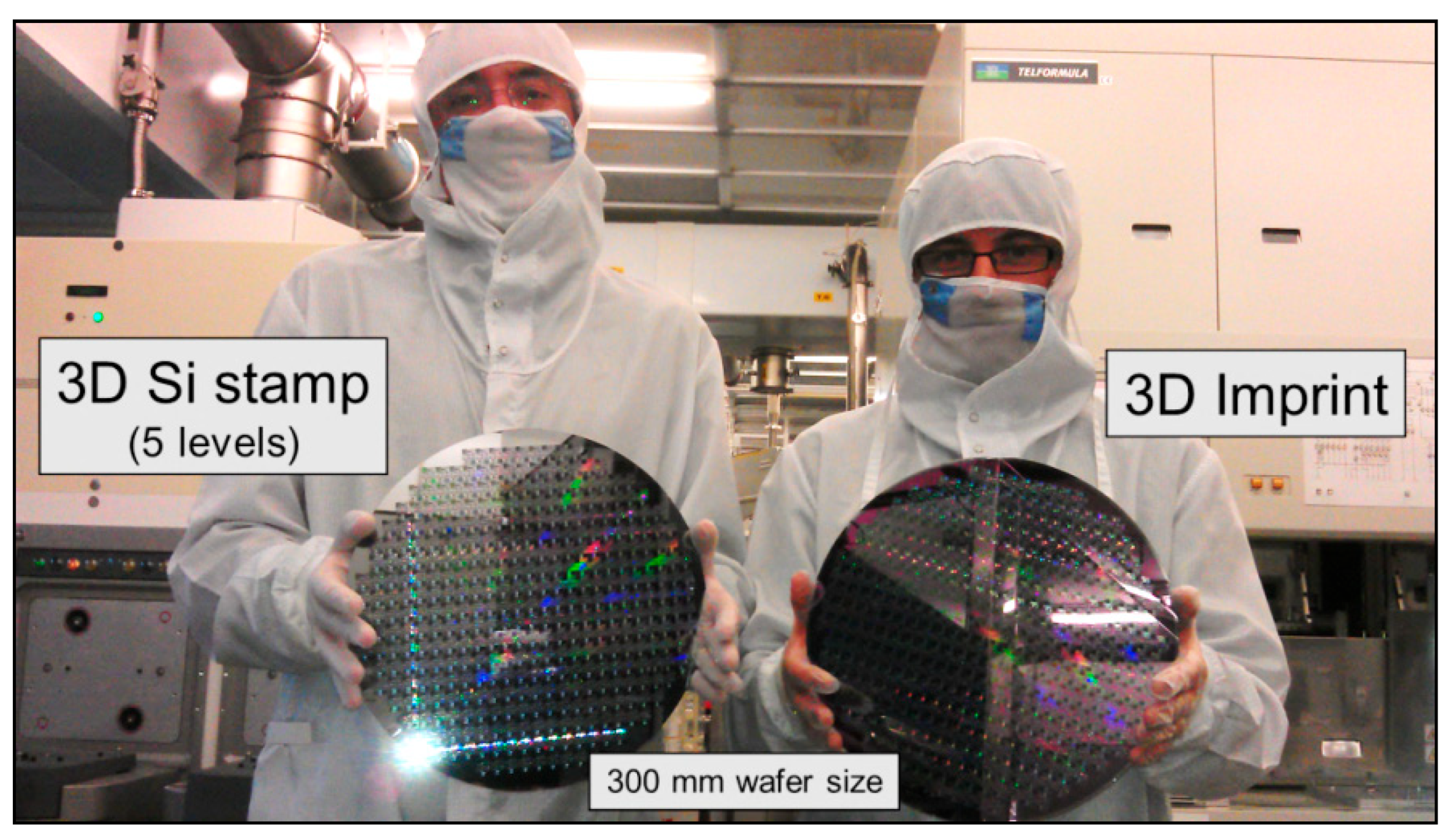
  • Full-wafer single imprint employs a stamp with the same size as the substrate, e.g., a wafer-like substrate. Then the entire pattern of the stamp can be transferred in one step, like in mask aligners. Such large stamps can be produced by tiling smaller stamps together by recombination but also by using large-area processes such as interference lithography or DUV-PL (see Figure 4). Full-wafer single imprint has been developed for T-NIL and UV-NIL.
  • Step-and-repeat (S&R) imprint processes are needed if a large-area stamp is not available or is too expensive or alignment cannot be assured over a large area. S&R NIL uses a stamp that is smaller than the substrate. By moving the stamp after imprinting to the adjacent area, with minimized stitching, the full surface can be sequentially covered with smaller, identical patterns until the entire wafer is fully covered with a regular array. S&R NIL has been developed for T-NIL and UV-NIL. In contrast to modern stepper-based PL, where a demagnified pattern of a mask is projected onto the substrate, S&R NIL requires high control of temperature or UV straylight, since imprinting over areas that have already been imprinted will result in a loss of structures or in a non-transfer of the pattern. Pick-and-place enables the use of individual stamps for different areas but is rarely used.
A specific novelty to using S&R processes for NIL is the dispensing of the UV-curable, low-viscosity resist not by spin-coating a homogeneous film but by ink-jetting droplets of liquid resin. This allows for drop-on-demand dispensing with specific density patterns that are adapted to the stamp design, enabling the use of hard stamps for resist films with good control of residual-layer thickness. Since it was first adapted to IC-chip manufacturing using S&R, it was coined step-and-flash IL (SFIL) and later renamed jet-and-flash IL (JFIL). It is exclusively used by Austin-based Molecular Imprints (MIIs), since 2014 Canon Nanotechnologies (CNT) (Austin, TX, USA, https://global.canon/en/technology/nil-2023.html (accessed on 7 July 2025)); see Section 3.2 Jet-and-flash imprint lithography and Section 4.2.1 IC-chip manufacturing [30,31,35]. To avoid variations in viscosity due to evaporation of the solvent, the resin is dispensed just before each imprint step; then the stamp is brought into contact, and the resist droplets are immediately spread onto a continuous film and imprinted within a fraction of a second [25,36].
Stamp copying can be both based on direct imprint and pattern transfer imprint. Direct imprint results in a copy with inverse (negative) polarity of the stamp. Therefore, a second copy might be needed to obtain the original positive polarity. The same applies for pattern transfer imprint if the resist pattern is used as the masking layer in an anisotropic etching process. By casting from an imprinted resist layer, a replica with the same polarity can be obtained. Copies can be characterized by “generations”, i.e., the original is named 0th gen. and the next copy the 1st gen., and the 2nd gen. has the same polarity as the original.

2.5. Continuous Processing

Standard imprint processes are sequential and stationary because every process follows a process sequence that is simultaneous in terms of location and time, with well-defined start and end. Processes such as roll-to-roll or reel-to-reel (R2R) are continuous and non-simultaneous. E.g., in thermal R2R-NIL, part of the substrate is heated up while another part is cooled down. Therefore, the stamp and the substrate are “continuous”, e.g., because a roll covered with a surface pattern is used to pattern an extended polymer film. Variants such as roll-to-plate (R2P) and plate-to-roll (P2R) NIL, or even SCIL, are partially continuous and use sequential process steps. With stamps bent around a roll, printing is performed in the so-called “nip”, the area of the closest gap between the two rotating cylinders, simply by squeezing a thin substrate between the patterned roll and a counter roll and repeating the pattern of its circumference during several revolutions:
  • In R2R-NIL the pattern of a rotating cylinder or a belt is transferred onto a flexible material such as polymeric (plastics) or metal films. Since the stamp is often made from a flat, flexible film that must be wrapped around a cylinder, the main challenge is to pattern the cylinder without a gap, which, otherwise, according to the application, can lead to seamlines, e.g., within long-distance optical elements. Often the term “roll embossing” is employed. R2R is better suited for large-area display devices but less compatible with thin resist layers and pattern transfer.
  • R2P-NIL transfers the pattern of a roller stamp onto a flat substrate, and in P2R-NIL, a flat stamp is imprinted on continuous film. This needs to be performed in a discontinuous way using S&R. R2P is more appropriate for lithography-related processes and has already been adopted for wafer-level NIL, e.g., for AR/VR device HVM.
R2R processes enable continuous processing, like in newspaper printing. Once a dynamic equilibrium is established, constant quality can be achieved over a large quantity of devices. This makes R2R processes suitable for increasing throughput, since overhead times (the alignment, heating, and cooling of plates) are eliminated because the related processes are implemented inline. R2R processes are physically identical to sequential and stationary processing and require similar times for mold filling; therefore, imprint times have to be long enough so that all patterns are replicated (either by employing slow speed and long nips or by using a belt instead of a cylinder). R2R-NIL has been developed for T-NIL and UV-NIL, by including heating or exposure systems at the locations where patterns are formed. R2R processes have the advantages of soft NIL and S&R NIL but need good control of process parameters and dynamic parameter optimization [37].

2.6. Hybrid Processes and Materials

Due to its mechanical approach and variety of materials that are moldable, NIL is destined for hybrid processing, i.e., combinations of processes, e.g., NIL and PL:
  • Combined nanoimprint and photolithography (CNP) is a process that was established to combine thermal NIL in a low-viscosity thermoplastic resist at moderate temperature and a consecutive UV-curing step that hardens the material by flood exposure. Obducat (Lund, Sweden, https://www.obducat.com/ (accessed on 7 July 2025)) uses a new stamp copy for each individual imprint, enabling the reduction in particle contamination of working stamps by incorporation using the so-called simultaneous thermal and UV (STU) imprint process and intermediate polymer stamps (IPSs). In the case where a stamp with an integrated absorber pattern is used, e.g., at the protruding elements of the stamp, crosslinking can be prohibited at the imprinted lower parts of the resist (where the light is blocked by the absorber), and the non-cured residual layer can be removed by chemical development [2,38,39].
  • Reversal imprint (R-NIL) is a technique where a resist is patterned via NIL, released from the underlying surface, and attached to another surface or already imprinted resist structure by bonding. Thus, multiple layers can be stacked, or resist structures can be transferred to surfaces that cannot serve as the imprinted substrate (e.g., due to mechanical restrictions) [40]. Similar approaches are now established for planarization on non-flat surface patterns, e.g., by droplet-based dispensing.
  • Combination of NIL, electron beam, DUV exposure, and localized thermal reflow, enabled by local variation in the thermoplastic properties of polymeric resists, creates surfaces with various patterns not achievable with PL alone, e.g., slopes instead of vertical sidewalls. This process is called TASTE (thermally activated selective topography equilibration) [41] and can be used to add molded surface patterns on polymeric 3D structures.
  • Hybrid materials are, e.g., inorganic–organic hybrid polymers (e.g., UV-curable Ormocers and organically modified ceramics) that combine the advantages of polymers with, e.g., the hardness or the functionality of inorganic materials. They can be used for optical applications but also as stamp copies. Furthermore, titania (TiO2) and silicon carbide (SiC) nanoparticles can be patterned, either directly or within a polymer matrix, and sintered into high-NA lightguides for AR/VR applications [42,43].
  • Stamps typically contain recessed and protruding features, i.e., flat areas with vertical sidewalls separating the two levels. Protrusions press materials downwards during imprint, thus resulting in lateral squeeze flow that enables the sinking of the stamp. The material flowing to the side fills the recessed areas that constitute the cavities in the stamps during imprint. Multi-level stamps contain several flat levels. Typically, the front protrusion must sit on larger protrusions. Such stamps enable the patterning of stepped resist structures and make it possible, e.g., to employ a self-aligned imprint lithography (SAIL) process, e.g., when the resist pattern is thinned down multiple times, each time followed by individual pattern transfer steps. SAIL was developed by HP for R2R processes for printed electronics. In the dual-damascene process, instead of a resist, the dielectric separating the wires of the interconnect layer of a chip is patterned, and the copper wires are created by electroplating [44,45].
  • Directed self-assembly (DSA) of block copolymers (BCPs) is a way to enhance resolution of stamps or structures intended for pattern transfer. Although NIL has shown resolution down to single nanometer and even below, fabricating large-area stamps with sub-10 nm features is difficult and time-consuming. Thus, a combination of top-down, bottom-up processing was favored using DSA. Lower-resolution patterns are fabricated by top-down lithographic methods such as EBL, and BCPs with defined blocks of hydrophilic and hydrophobic segments that are smaller than these “rails” enable the generation of bottom-up patterns between these rails that are ordering the BCPs with high reproducibility and even the ability to heal defects in proximity. Other techniques pattern block polymers directly by using mechanical molding techniques, thus enabling the alignment of polymer chains and molecules [46,47]. If the blocks are made from different polymers, e.g., PMMA and polystyrene, their difference in etch resistance in reactive ion etching processes can be used to generate high-resolution resist patterns.
Hybrid approaches add complexity to process flow but are particularly favorable for the fabrication of expensive high-resolution stamps that can then be copied and multiplied. If hybrid approaches are used for HVM, they can be energy-saving or, in the case of CNP, SAIL, or dual-damascene processing, reduce the number of patterning steps, avoid complex alignment, and likely contribute to enhancing NIL’s ability to create solutions that are sustainable and real alternatives to processes that, until now, have used up a lot of resources.

3. Tools and Materials

3.1. Full-Wafer Single Imprint and S&R Imprint Tools with Hard and Soft Elements

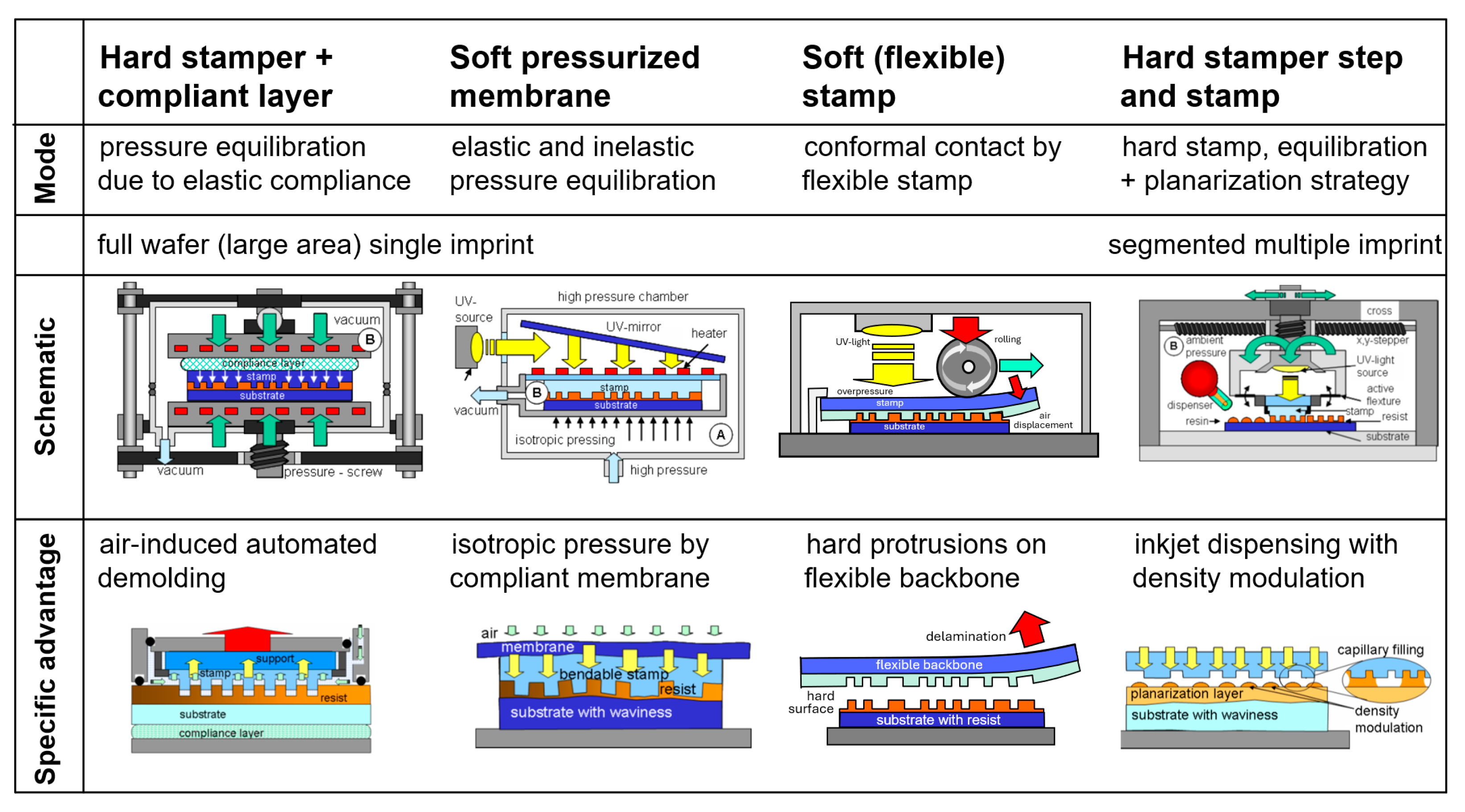
The first tools were modified pill presses, anodic bonders, or converted mask aligners, e.g., those by SUSS (Garching, Germany, https://www.suss.com/ (accessed on 7 July 2025)) and EVG (St. Florian am Inn, Austria, https://www.evgroup.com/ (accessed on 7 July 2025)) [2,5]. In all cases, the aim was to achieve homogeneous contact between the stamp and the resist-coated substrate, which needed to be maintained while the molding was going on and the resist was not yet hardened. In the case of mask aligners and anodic bonders, their alignment capability was instrumental in achieving overlay. Today, more specialized tools for NIL use pressurized membranes behind the stamp or moving rolls behind a flat stamp. This allows for single-point or line contact before reaching conformal contact over the entire surface, thus maintaining homogeneous pressure and even the defined delamination of the stamp from the molded resist. Specific membrane-based solutions are provided by NanoNex (Air Cushion Press (ACP)) (Monmouth Junction, NJ, USA, https://nanonex.com/ (accessed on 7 July 2025)), Obducat (SoftPress) (Lund, Sweden, https://www.obducat.com/ (accessed on 7 July 2025)), SCIL Solutions (Eindhoven, The Netherlands, https://scil-nano.com/ (accessed on 7 July 2025)), and NILT (Kongens Lyngby, Denmark, https://www.nilt.com/ (accessed on 7 July 2025)), later adopted by SUSS and EVG. Also, solutions allowing for sub-10 nm alignment have been developed. Particularly interesting are solutions using soft elements, i.e., bendable stamps, which have now also reached sub-100 nm resolution due to material developments and hybrid approaches. Although different in terms of process and pressure, it must be noted that all NIL machines include hard and soft elements, enabling both alignment and conformal imprint over non-perfect substrate surfaces. Some of these solutions are presented in Figure 5 and are detailed as follows:
  • Imprint machines or presses enable manual, semi-automated, or automated process cycles. NIL tools are mechanically “simpler” than micro-embossing tools for high-aspect-ratio microstructures (HARMSTs), which require high mechanical stiffness to ensure purely vertical movement during molding and mold separation, and vacuum to avoid trapped air. NIL presses require vertical flexibility, i.e., membrane-based solutions that enable conformal contact and peeling. However, like projection-based steppers, alignment requirements of sub-100 nm or even in the nm range make NIL presses mechanically challenging. This involves mechanisms for approaching; pressing; displacement, dissolution, or compaction of air; demolding; and handling. For T-NIL, due to high viscosity, a pressure of up to 10 MPa (100 bar/1’450 psi) for squeeze flow is required, for UV-NIL, and a low pressure of only 10 kPa (0.1 bar/1.5 psi) for capillary filling.
  • Imprint stamps can be hard (silicon, fused silica, nickel, diamond, etc.) or soft (PDMS with different shore hardness) or combine hard and soft elements (e.g., hard PDMS on a soft backbone, or a soft topographical layer on a polymer film). A rigid stamp requires flat substrates, a dust-free environment, tilt control, and precise vertical movement while maintaining lateral alignment. An opaque and transparent stamp with silicon oxide on top can be coated with fluorinated silanes with excellent antisticking properties. There are a variety of processes for manufacturing stamps in silicon with specific topographies, e.g., high aspect ratio (HAR; ratio of height/width) and grating with slanted ridges.
  • A resist is the intermediate material, used as a sacrificial layer, or a functional layer that is either directly created or transformed. It is defined by its chemical composition (e.g., chemistry of the polymer backbone and molecular weight) and by additives (photosensitive components, i.e., initiator, crosslinking agent, and solvent) and is characterized by its viscosity, etch resistance and selectivity with respect to the substrate, curing mechanism, and surface properties (good wetting during coating and good release and friction properties during demolding). PDMS, since it is gas-permeable, requires, as a stamp material, non-oxygen-inhibiting resists, i.e., which crosslink in the presence of oxygen. If non-gas-permeable materials such as fused silica are used as the stamp, they can imprint on oxygen-inhibiting resists, thus only hardening material in the gap between stamp surface and substrate, while squeezed-out material remains uncured. Further properties are refractive index, hardness, molecular weight, and glass transition, imprint (flow), and demolding temperatures.
For HVM, integrated solutions in which coating and pre- and postbaking are combined in cluster tools are required. This enables high reproducibility, high throughput, and low contamination due to automated handling and cassette systems, and even the exchange of damaged or contaminated stamps. Low defectivity is enabled by a reduction in particles in the global environment (flow boxes) but also by the micro-environment (local air flow curtains transporting particles away from the imprint area). Such solutions are provided by Canon, Obducat, NanoNex, EVG, SCIL Solutions, SUSS, and German Litho (Allershausen, Germany, https://www.germanlitho.com/ (accessed on 7 July 2025)).
Crucial to the success of high-resolution patterning is the availability of suitable stamps. In contrast to projection-type PL, NIL templates need to have the same resolution as the printed features. Today, most stamps are, similarly to the masks for PL, fabricated using scanning laser or electron-based direct write lithography (DWL). Care must be taken that stamps have vertical sidewalls and exhibit sufficient antiadhesive properties towards the resist. This is often accomplished by coating it with an ASL from fluorinated monomers. Due to 1X replication, future stamps will require parallelized, high-resolution serial patterning techniques for large areas such as advanced (multi-beam) EBL (e.g., by IMS Nanofabrication GmbH (Brunn am Gebirge, Austria, https://www.ims.co.at/ (accessed on 7 July 2025))) and scanning (multi-)probe lithography (SPL) for hydrogen desorption (Zyvex Labs (Richardson, TX, USA, https://www.zyvexlabs.com/ (accessed on 7 July 2025))) techniques [48].

3.2. Jet-and-Flash Imprint Lithography Tools

Similarly to the NIL tools enabling full-wafer single imprint, S&R NIL made use of flip-chip bonders and DUV steppers that were converted into sequential imprint machines with integrated heating or UV-exposure systems, vertical mechanisms for pressure build-up, lateral alignment, and tilt control (see Figure 6) [49,50].
The JFIL process cycle consists of resist dispensing, approaching the stamp using single contact, lateral alignment in liquid state, UV-flash exposure, and demolding. The current wafer format in HVM is 300 mm. The specific characteristics of JFIL are as follows:
  • JFIL uses a hard stamp (called die) with a patterned area of 26 × 33 mm2, which is adapted to the size of a PL exposure field in the industrial HVM of IC chips. It is made from a 6025 semi-standard, 6″ × 6″ × 0.25″ fused silica photomask template with a thinned-down central area that allows for flexibility and single contact in the center, enabling to squeeze air out to the sides.
  • The resist is ink-jetted by drop-on-demand dispensing using a multi-nozzle print head. This allows for the rapid coating of the area that will be imprinted right afterwards and for density adaption according to the ratio of cavities to be filled. Alignment is performed in the liquid state, i.e., after the resist droplets are spread and merged.
  • A micro-environment around the imprint area is created for local removal of dust particles, to reduce contamination by abrasion of ceramic bearings and filter particles from resists.
  • Stamp copying is performed in a separate tool and requires a resist patterning process with consecutive pattern transfer such as reactive ion etching.
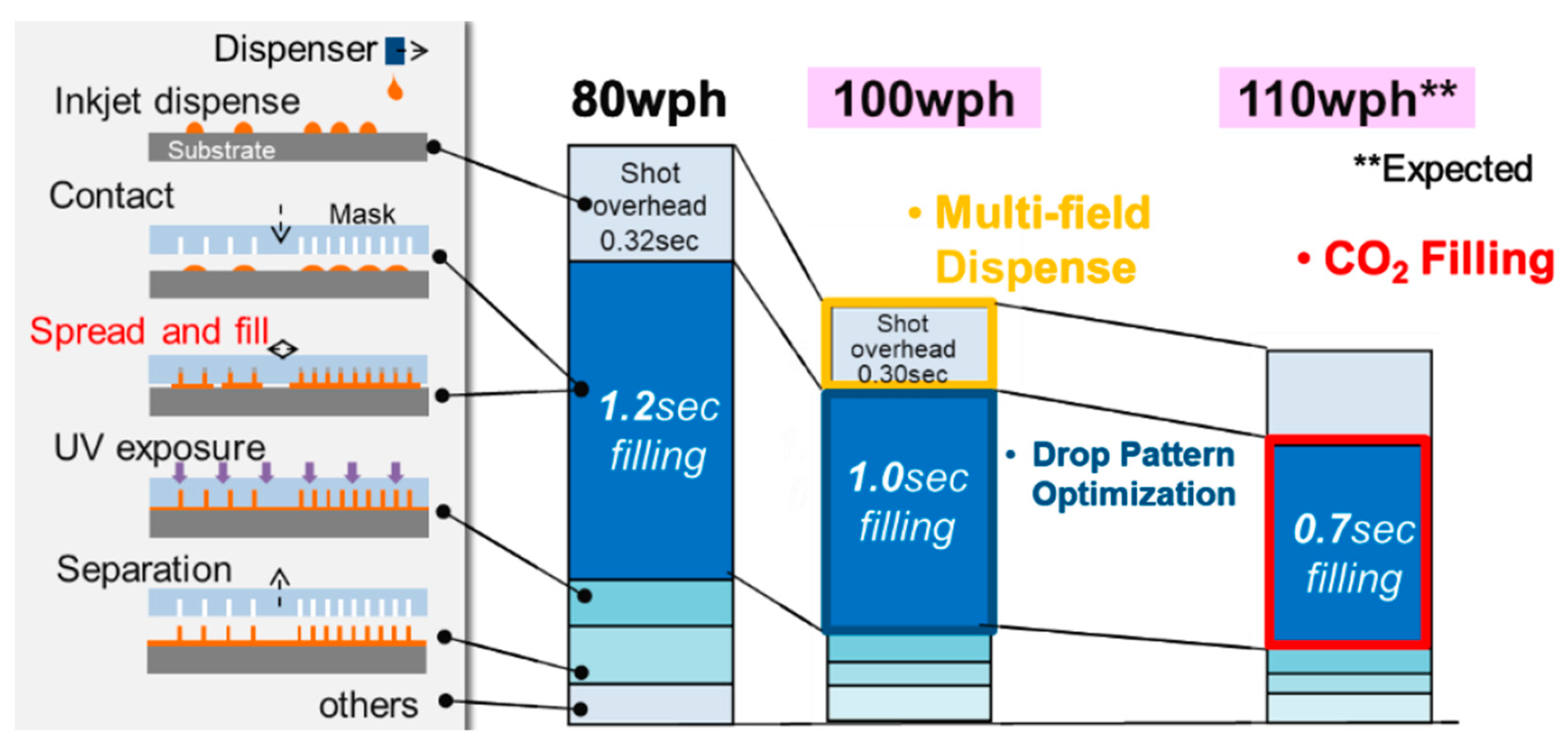
Canon is the only company offering NIL as an alternative to EUV lithography, using its proprietary SFIL process. The 248 nm and 193 nm (immersion) DUV tools are still the main workhorses in the HVM of semiconductor IC chips. The target value for a four-station NZ2C tool is (status 2025) a throughput of 110 wph (wafers/hour) with an alignment accuracy of 2 nm, which is the requirement for HVM for DRAM fabrication (see Figure 7) [51,52,53,54,55]. For a stamp lifetime of 2000 wafers which meet a defect spec of 0.10 defects/cm2, the particle adder target is 1 defect every 10’000 wafers. This is now being achieved in multiple stations. NIL has not yet entered HVM in 2025.

4. Applications

4.1. General

The first applications attracting huge attention for NIL with its sub-10 nm resolution were IC chips and bit-patterned media (BPM), with the former addressing the limitations of PL in the multi-level-based patterning of transistors and the latter addressing the need to enhance data volume on magnetic discs by creating a high-resolution topographical pattern in a single-level patterning step. Other applications have used NIL for the fabrication of integrated polymeric waveguides, grating couplers, and polarization gratings. Applications can be divided into two main categories [5]:
  • Pattern transfer applications are those employing EBL and PL, because the imprinted structure is used as a temporary masking layer (“resist”), i.e., a sacrificial layer that is removed after the pattern transfer process is finished. Both IC chips and BPM belong to this category.
  • Direct imprint applications are based on “resist-less” processes. The imprinted pattern adds functionality to the surface of a bulky device, which is the product. Often these are polymer devices or thin polymer films on top of a substrate.
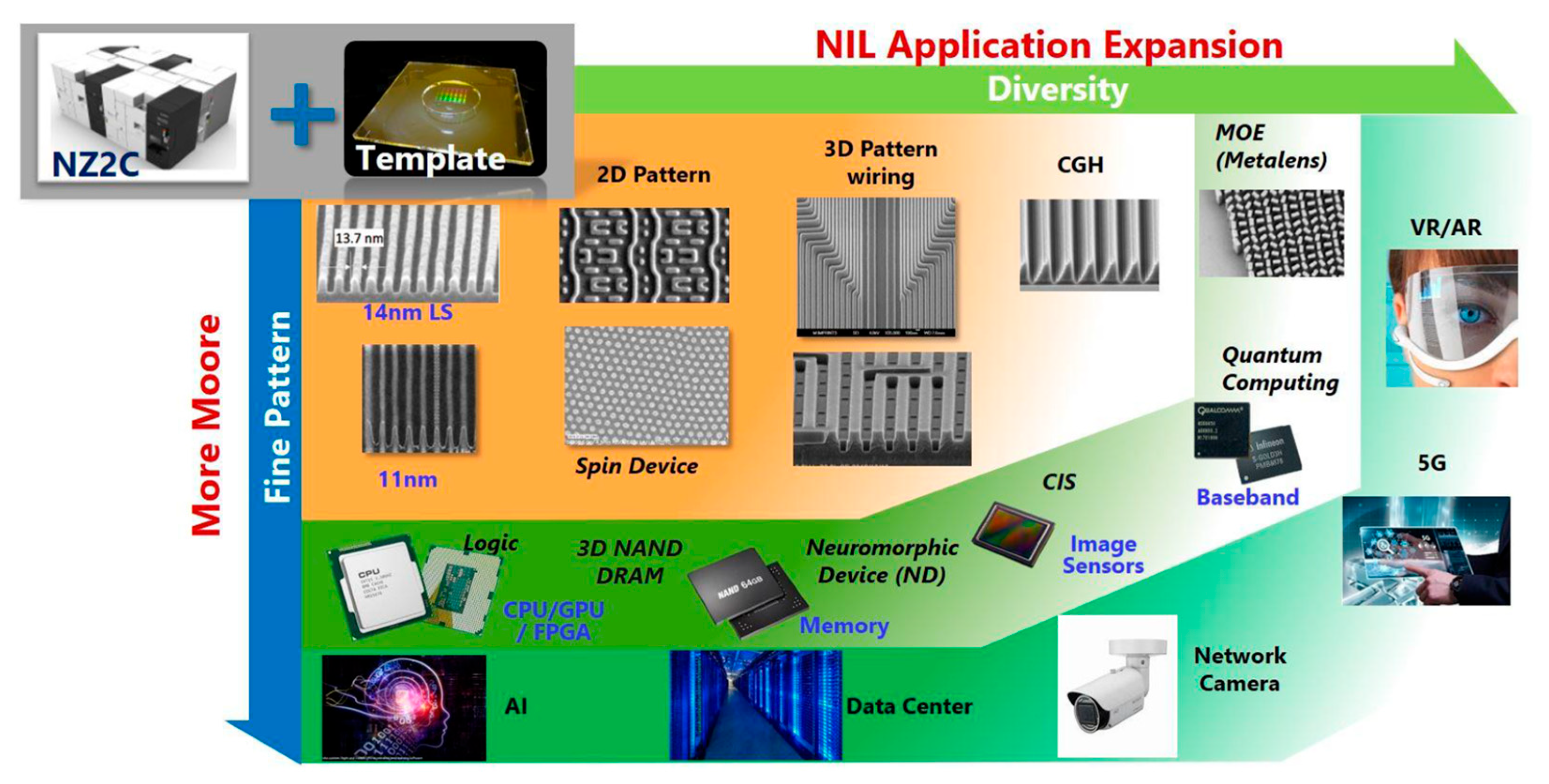
Because NIL has both aspects of classical lithography, i.e., PL (as a parallel method for HVM) and EBL (as a serial method mostly dedicated to mask making and research), but also of molding techniques (diffractive gratings, holograms, antireflective, and superhydrophobic surfaces), NIL needs to be considered a toolbox rather than a single technique. In addition to PL, NIL will also be considered for some applications in which lithography is too costly and does not provide sufficient resolution or throughput. This is particularly true for large-area applications such as magnetic media, as in the surfaces of hard disks, where patterning has not been used until now and costs need to be kept within a few cents per device [5]. Several applications are summarized in Figure 8.

4.2. Applications Based on Imprint on Resists for Pattern Transfer

4.2.1. IC-Chip Manufacturing

From its initial demonstration of 10 nm imprint capabilities, NIL was expected to become next-generation lithography (NGL) intended for the HVM of IC chips, where photolithography (PL) was used since the 1960s. In 1995, when PL resolution using DUV 248 nm was at 350 nm node (half-pitch) patterning, NIL was considered an alternative for high-end PL and X-ray proximity lithography (XRL; wavelength below 1 nm). NIL was, therefore, many times better than the actual PL and even below the anticipated resolution limit of XRL, thus presenting a solution to Moore’s law, which predicted a doubling of the number of transistors every 2 years, later adapted to 18 months. However, the industry did not adopt XRL and moved on to 193 nm DUV in 1998. In 2003, when 90 nm was in the industry, the International Technology Roadmap for Semiconductors (ITRS) included NIL as one of the NGL candidates for the 32 and 22 nm “nodes” (design resolution) [11], which boosted interest into this new technique, which was considered a paradigm change. By 2009, it had been included in the ITRS at the 22, 16, and 11 nm nodes (at that time, nodes were not equivalent to resolution anymore). Due to an enormous effort to create plasma sources and projection optics for 13.5 nm light, EUV lithography has finally been adopted by the industry as the successor to 193 nm DUV immersion PL. It became the new workhorse for high-end HVM chip manufacturing at the enhanced 7 nm logic node in 2019 (14 nm resolution), with up to 220 wafers per hour (currently ASML’s NXE 3800 EUV system (Veldhoven, The Netherlands, https://www.asml.com/ (accessed on 7 July 2025))) [35,48]. It seems that the chip industry will continue to use EUV for smaller nodes, even with the cost of a current tool of USD 200–400 million and the cost of a mask set of USD 38 million. NIL is currently capable of producing chips with 5 nm technology and may eventually reach 2 nm nodes, according to Canon. ASML’s high-numerical-aperture (NA) tool (with an NA of 0.55 instead of the current NA of 0.33) will target a resolution of 8 nm, and further improvements may require even smaller wavelengths and double or even quadruple patterning (i.e., four masking steps for one layer in a complex chip design), as it was required by late DUV PL. NIL will, however, be a more cost-effective and energy-saving alternative, with a JFIL tool cost of USD 20–40 million (currently Canon’s FPA-1200NZ2C) [54,55]. And although its defectivity and overlay issues are still seen as prohibitive, its advantage is that NIL does not need expensive optical projection systems and high-power plasma sources for the generation of 13.5 nm EUV light and their huge optical losses in the imaging system. The main bottleneck for NIL is, however, that 1X stamps must be fabricated with features that are four–five times smaller than an optical projection mask. At the same time, NIL requires stamp-copying techniques to “enhance” the lifetime of stamps in manufacturing due to wear and contamination. Its 1X copying capability is, at the same time, one of the big benefits of NIL, enabling HVM in clusters of several JFIL tools using identical stamps. Even if NIL will not be considered for the HVM of top-node chips anymore, it will be a more cost-effective alternative to EUV lithography and even for older PL types, such as 193 nm and 248 nm systems. The first application will be likely be NAND storage, which is an HVM application with relaxed but still challenging requirements in terms of overlay and defectivity. DRAM and logic, which are more challenging due to their high demand for low defectivity and overlay, will also be considered. Beyond memory and logic, the covered device space includes CMOS image sensors, diffractive optical elements (DOEs), and meta-optical elements (MOEs) for semiconductor-based applications that evolve as future application markets (Figure 8) [53]. Such applications require different performance with respect to overlay, defectivity, and throughput.

4.2.2. Non-IC-Chip Manufacturing

NIL has proven successful in applications different from semiconductor manufacturing, where extreme resolution and the overlay do not play a big role [56].
Hard-disk drives (HDDs) with enhanced storage capacity have been among the first applications envisaging NIL for HVM. As a solution for reducing crosstalk from neighboring magnetic domains in a continuous magnetic film, either individual dots must be patterned (Figure 1), or the film must be coated over the surface topography with air gaps between dots, thus realizing individually separated magnetic storage elements (BPM). NIL needs to pattern small (sub-20 nm) lands over an entire disk surface (2 or 3 inches), typically made from aluminum or glass. The requirements in terms of overlay and defectivity are relaxed, since only single-layer patterning is required and missing bits can be compensated for. All major HDD companies (Seagate (Dublin, Ireland, https://www.seagate.com/ (accessed on 7 July 2025))/Samsung (Suwon, South Korea, https://www.samsung.com/ch/memory-storage/ (accessed on 7 July 2025)), Western Digital (San José, CA, USA, https://www.westerndigital.com (accessed on 7 July 2025))/Hitachi, Toshiba (Shibaura, Minato, Tokyo, Japan, https://www.toshiba-storage.com/ (accessed on 7 July 2025)), etc.) have run BPM programs [57] but, because of other priorities, have put BPM on hold. High-resolution masters (sub-20 nm) were fabricated using EBL and resolution enhancement by DSA of BCP spacer etching. The combination of top-down and bottom-up nano-approaches was novel in the industry and addressed an area where high-resolution EBL does not provide enough throughout.
Functional resist patterning offers solutions for micro- and nano-optics (e.g., antireflective gratings on photovoltaic cells with improved efficiency, wire-grid polarizers, and backlight and frontlight illumination of screens and light panels), plasmonic and photonic devices, and metalenses [43,58,59,60]. Today, most light emitting diodes (LEDs) are produced on micropatterned sapphire substrates (µPSSs), which are needed to grow GaN layers with low defects and to enhance light extraction. The resolutions currently needed are in the micrometer range but are now also extended to nanopatterned substrates (nPSSs) [61]. The big advantage of NIL is the possibility to print over defects in current 100 mm sapphire substrates using flexible stamps. Tens of thousands of chips 100 × 100 µm2 in size can be patterned in a single-layer imprint process, making NIL a cost-effective solution. In contrast to this, if NIL is used in housing applications, e.g., for light control and redirection, antireflection, or reduction in contamination, large-area imprint is required for entire glass windows.
Bio-applications (for DNA analysis or as templates for cell growth) will also benefit from the introduction of NIL. The HVM of chips for DNA sequencing using plasmonic nanostructures is performed by Illumina (San Diego, CA, USA, https://www.illumina.com/ (accessed on 7 July 2025)). The markets are currently still much smaller than those of IC-chip HVM; however, they are expected to grow rapidly.

4.3. Applications Based on Imprint on Functional Materials

4.3.1. Surface-Patterned Polymer Devices

Thanks to the variety of optical effects possible with diffractive gratings or specific surface textures, numerous applications seem possible using the imprint of polymer films or coatings on polymer or glass films. If these or similar effects are found in nature, they are called biomimetic or bionic surfaces. Surface gratings often create multiple effects, e.g., antiwetting and color effects. Color effects can be avoided if the grating periods are so small (sub-wavelength) that the first-order diffraction of visible wavelengths is above 90° and all light is transmitted in the zeroth order without dispersion. Such effects are further detailed as follows:
  • Surface textures create effects that are based on topography by enlarging the surface and creating undercuts with large air pockets and directional patterns such as sawtooth structures. These include “gecko” surfaces with engineered adhesion, “sharkskin” surfaces that reduce drag in water, and antifog, anti-contamination, and anti-fouling applications. The so-called Lotus effect is a combination of micro- and nanostructures with a hydrophobic surface property that keeps the leaves of the Lotus plant free from contamination and dust. They reduce the contact area between particles and the surface and enlarges the water contact angle, which reduces the ability of water to wet surfaces. This enables the rolling of water droplets, which drags particles and fungi before they can infect the leaf.
  • Diffractive gratings create antireflective or polarizing effects. The moth eye effect is achieved with arrays of pillars, which, due to their sub-wavelength period and tapered shape, create an adiabatic refractive index transition from the air to the eye that reduces reflectivity, without creating color effects. In contrast to this, a large interference grating arranged in 3D pillars, with small lateral domains, can be engineered by mimicking the “morpho blue” effect with structural rather than pigment-based coloring (“physical colors”). The blue color in butterfly wings is, in comparison to simple interference gratings, present in different directions. A new field is represented by metalenses, which enable the fabrication of “flat optics”, which enable a wide-angled field of view without a bulky set of stacked refractive lenses.
Often, compromises are needed because functional structures in biomaterials are often not hard enough to sustain permanent use in harsh environments. In nature, this is often solved by regeneration and growth of new material (chitin, wax, etc.). In industry, hard materials (e.g., diamond-like coatings) that enable use with low wear are required.

4.3.2. High-NA Waveguides for AR/VR Applications and Structural Colors

Information is transmitted via screens and projection displays. The current ascent of AR/VR (augmented and virtual reality) devices require smart glasses, goggles, or headsets that feature integrated waveguides and gratings. They transmit images or information from projectors into the eyeball while allowing one to see the environment through glasses like in a head-up display. This should be performed in three colors and for a large field of view, with high contrast and with a low scattering of light. The current waveguide couplers are constituted of slanted gratings (i.e., a multitude of inclined ridges with undercuts). NIL, with its demolding constraint, i.e., topographies without undercuts, is only able to fulfil this requirement if stamps with flexible (“soft”) surface structures are molded into a functional material, which is stiff enough not to collapse during imprint and flexible enough to deform during demolding, after the material has been solidified. Instead of the direct patterning of functional materials, slanted gratings can also be fabricated using resists. While, in the first case, a functional material (organic, inorganic, or hybrid) that provides high NA either directly or after a sintering step is imprinted, in the latter case, resist patterning is followed by inclined anisotropic reactive ion-beam etching (RIBE) into an underlying high-NA, inorganic glass-like material like TiO2 or SiC. Real (freeform) 3D-printing is still difficult to achieve using NIL; however, combinations of techniques, soft and deformable stamps, and reversal imprint are techniques that enable to add 3D characteristics to NIL despite the demolding constraint.

5. Conclusions and Prospects

After 30 years of development [6], NIL is now a mature patterning process that is already employed on an industrial scale for LED manufacturing and biochips. Other applications have been tested for production, but often, companies do not disclose whether they have entered HVM. Patterned magnetic media have been put on hold. In IC-chip HVM, NIL has become the second option after the energy-consuming EUV-PL, with EUV lithography becoming the exclusive workhorse for TSMC (Hsinchu, Taiwan, https://www.tsmc.com/ (accessed on 7 July 2025)) in Taiwan, Samsung in Korea, or Intel (Leixlip, Kildare, Ireland, https://www.intel.ie/ (accessed on 7 July 2025)) in Ireland. For IC chips, NIL was developed by MII up to maturity in HVM, and Canon continues to challenge ASML with its proprietary JFIL process, thus keeping Moore’s law alive. They contributed to the development of large-area high-resolution patterning and related processes such as the inkjet coating of resists and are therefore highly relevant for an entry in this encyclopedia. While IC-chip HVM is the driver of high-end lithography with highly standardized but challenging multi-level patterning processes that require high throughput, high overlay accuracy, low defectivity, high reliability, and tools that work in ultra-high-quality cleanroom processes, NIL will continue to drive other key industrial domains. In comparison to EUV lithography, NIL does not exclusively serve the semiconductor market and is therefore considered for applications that are “More than Moore”. It will likely enter areas in which EUV lithography is too expensive, not available, not flexible (substrates, materials, surface topography, etc.), or not scalable enough. Future progress will depend on applications that need simple solutions (e.g., single-layer patterning with regular patterns) for large areas to be imprinted quickly, reliably, and with few defects.
NIL is here to stay, but EUV lithography will take most of the share of IC-chip HVM. EUV lithography will never be employed in areas outside the HVM of semiconductor IC chips because it is too specialized and expensive for non-IC applications. NIL, apart from areas where its capability is considered unique, e.g., for the patterning of functional materials by molding, will be competing with other lithographic techniques. These are, e.g., either highly parallelized, direct write techniques like EBL and SPL or parallel large-area displacement Talbot lithography (DTL). They all have their specific advantages in terms of minimum resolution, patterning over topography, large area and throughput, versatility of structures, flexibility, ability to pattern functional materials, and 3D morphology, e.g., structures with undercuts or continuous topographies. Pattern transfer processes are often expensive but have proven low defectivity. The direct imprint of, e.g., TiO2 or SiC nanoparticles for high-refractive-index applications, followed by atomic layer deposition (ALD) or sintering, has shown tremendous progress but relies on materials with defined properties. NIL enables the imprint of resists for pattern transfer but also direct imprint on functional materials. Meanwhile, the broad variants of processes will make new applications possible. NIL can be adapted to large areas, non-flat surfaces, and functional materials. For this, custom tools and processes need to be provided, different from the original NIL process. Many bio-applications, such as surface patterns for enabling DNA sequencing and controlling cell growth, were—until recently—unthinkable. They profit from a toolbox for stamp manufacturing that has been established during recent years and includes 3D surface patterning and replication by different molding processes, such as injection molding and roll embossing [16]. Hence, nanoimprint is mo(o)re than lithography. All solutions need to tackle all requirements in terms of master production (origination), tooling (production of working stamps), imprint, and pattern transfer (conversion into the desired material). Particularly challenging will be the fabrication of seamless large-area stamps, the use of stamps in HVM (with more than 10’000 imprints per stamp), and inline defect identification and control.
NIL was and still is known for its high resolution, unmatched by other parallel top-down methods, which is possible because mechanical displacement can be very well controlled within nanometers and even below. The technical principles are old, but the possibility to pattern down to sub-10 nm resolution at a time when PL was considering 50 nm resolution as the end of structuring was in fact “an old story in modern times” [2]. Today, after 30 years of development and with IC-chip HVM approaching 10 nm resolution, NIL faces new challenges, e.g., the huge variety of processes and lack of standardization. NIL is mostly advertised for its cost-effectiveness, particularly in comparison to other high-resolution techniques. This is complemented by the freedom of materials, scalability of area, bonding, transfer and build-up of entire layer, and compatibility with S&R and R2R techniques. In the future, similarly to inkjet printing, NIL will be employed in 3D printing, on non-flat surfaces such as eyeglass lenses, but also complex consumer goods. This will be performed by using robots. Then, it will not be the question of “nanoimprint lithography—2D or not 2D” anymore [16] but “I (im)print, therefore I am”.

Funding

This research received no external funding.

Institutional Review Board Statement

Not applicable.

Informed Consent Statement

Not applicable.

Data Availability Statement

No new data were created or analyzed in this study. Data sharing is not applicable to this article.

Acknowledgments

Over the last 30 years, the NIL process has been developed due to the individual and joint efforts of many researchers, engineers, and technologists around the world, with communities in the USA, Europe, and Asia. NIL was neither created for a niche application nor for the HVM of semiconductor IC chips alone. Both research communities and industrial players have contributed to the ascent of NIL, which has become one of the manufacturing techniques which will open markets for nanopatterned products. My heartful thanks go to all researchers working collaboratively on the understanding of process issues and development of the toolbox for NIL, particularly to those who worked on the NaPa or NaPANIL library of processes [62]. Most of the development is now performed in industry, and I am glad that I could contribute. In fact, our first experiments using NIL were published under the term “hot embossing lithography” in 1998, which relates to other replication techniques known for a long time, including the hot embossing of DOEs [1,63,64,65,66]. Several reviews and books present overviews and state of the art on patterning techniques and particularly on NIL. Apart from the scientific literature, technological development can also be found in different sources; e.g., there are more patents on NIL processes than scientific publications. The reader is advised to scan the literature for other terms, such as embossing, molding, LiGA-technology, and printed electronics. The basis of this article is the entry into NanoPedia.org 2017 © Helmut Schift and has been updated and enlarged. The webpage has ceased to exist (status: 1 July 2025).

Conflicts of Interest

The author declares no conflicts of interest.

Abbreviations

The following abbreviations are used in this manuscript:
ASLantisticking layer, a monomolecular layer of (perfluorinated) antiadhesive silanes
AR/VRaugmented/virtual reality, requiring goggles with integrated waveguides and gratings
BCPblock copolymer, with alternating segments of hydrophilic or hydrophobic properties
BPMbit-patterned media
CNPcombined nanoimprint and photolithography, using stamps with integrated masks
DSAdirected self-assembly, enabling combination of top-down and bottom-up approaches
DUVdeep ultraviolet (248 nm or 193 nm and immersion 193 nm)
EBLelectron-beam lithography
EUVextreme ultraviolet (13.5 nm), since 2019 used as wavelength for chip manufacturing
HVMhigh-volume manufacturing
IRDSInternational Roadmap for Devices and Systems (since 2016)
ITRSInternational Technology Roadmap for Semiconductors (1993–2017), succeeded by IRDS
JFILjet-and-flash imprint lithography (Molecular Imprints Canon Nanotechnology)
LiGAprocess sequence of lithography, electroforming, and molding (German acronym)
Moore’s lawGordon Moore, CEO of Intel, noted in 1965 that the number of components per IC had been doubling every year. His prediction has held since 1975 and has become known as a law. It has been used in the semiconductor industry to guide long-term planning and to set targets for research and development, including resolution in lithography
µCPmicrocontact printing, a soft lithography method
NILnanoimprint lithography
NNTInternational Conference on Nanoimprint and Nanoprint Technology, since 2002
PDMSpoly(dimethyl siloxane), silicone rubber used for soft lithography
PLphotolithography, using photons to pattern resists
R2Rroll-to-roll, continuous patterning technique for films
SAILself-aligned imprint lithography by Hewlett Packard HP
SAMself-assembled monolayer, used for µCP
S&Rstep-and-repeat, used for enlargement of surfaces using small stamps
SCILsubstrate conformal imprint lithography (by Philips)
STUsimultaneous thermal and UV imprint using intermediate polymer stamps (IPSs)
T-NILthermal NIL, also known as heat-assisted NIL or hot embossing
UV-NILUV-assisted NIL, using UV light for curing liquid resists

References

  1. Heyderman, L.J.; Schift, H.; David, C.; Gobrecht, J.; Schweizer, T. Flow behaviour of thin polymer films used for hot embossing lithography. Microelectron. Eng. 2000, 54, 229–245. [Google Scholar] [CrossRef]
  2. Schift, H. Nanoimprint lithography: An old story in modern times? A review. J. Vac. Sci. Technol. B 2008, 26, 458–480. [Google Scholar] [CrossRef]
  3. Schift, H.; Kristensen, A. Nanoimprint lithography—Patterning resists using molding. In Handbook of Nanotechnology, 3rd ed.; Bhushan, B., Ed.; Springer: Berlin/Heidelberg, Germany, 2010; Chapter Part A/9; pp. 271–312. Available online: https://link.springer.com/chapter/10.1007/978-3-642-02525-9_9 (accessed on 7 July 2025).
  4. Schift, H.; Kristensen, A. Nanoimprint lithography—Patterning resists using molding. In Handbook of Nanotechnology, 4th ed.; Bhushan, B., Ed.; Springer: Berlin/Heidelberg, Germany, 2017; Chapter Part A/5; pp. 113–142. [Google Scholar]
  5. Resnick, D.; Schift, H. Nanoimprint lithography. In Microlithography—Science and Technology, 3rd ed.; Suzuki, K., Smith, B.W., Eds.; CRC Press: Boca Raton, FL, USA, 2020; Chapter 12; pp. 595–678. [Google Scholar]
  6. International Conference on Nanoimprint and Nanoprint (NNT). Available online: http://www.nntconf.org (accessed on 7 July 2025).
  7. Fujimori, S. Fine pattern fabrication by the molded mask method (nanoimprint lithography) in the 1970s. Jpn. J. Appl. Phys. 2009, 48, 06FH01. [Google Scholar] [CrossRef]
  8. Chou, S.Y.; Kraus, P.R.; Renstrom, P.J. Imprint of sub-25 nm vias and trenches in polymers. Appl. Phys. Lett. 1995, 67, 3114–3116. [Google Scholar] [CrossRef]
  9. Chou, S.Y.; Kraus, P.R.; Zhang, W.; Guo, L.; Zhuang, L. Sub-10 nm imprint lithography and applications. J. Vac. Sci. Technol. B 1997, 15, 2897–2903. [Google Scholar] [CrossRef]
  10. Haisma, J.; Verheijen, M.; van den Heuvel, K.; van den Berg, J. Mold-assisted lithography: A process for reliable pattern replication. J. Vac. Sci. Technol. B 1996, 14, 4124–4128. [Google Scholar] [CrossRef]
  11. Huang, G.T. 10 Emerging Technologies That Will Change the World. In MIT Technology Review; Technology Review Inc.: Cambridge, MA, USA, 2003; Available online: https://www.technologyreview.com/10-breakthrough-technologies/2003/ (accessed on 7 July 2025).
  12. Hua, F.; Sun, Y.; Gaur, A.; Meitl, M.A.; Bilhaut, L.; Rotkina, L.; Wang, J.; Geil, P.; Shim, M.; Rogers, J.A.; et al. Polymer imprint lithography with molecular-scale resolution. Nano Lett. 2004, 4, 2467–2471. [Google Scholar] [CrossRef]
  13. Tan, G.; Nozawa, Y.; Funabasama, T.; Koyama, K.; Mita, M.; Kaneko, S.; Komura, M.; Matsuda, A.; Yoshimoto, M. Atomic-scale thermal behavior of nanoimprinted 0.3 nm high step patterns on PMMA polymer sheets. Polym. J. 2016, 48, 225–227. [Google Scholar] [CrossRef]
  14. Chou, S.Y.; Keimel, C.; Gu, J. Ultrafast and direct imprint of nanostructures in silicon. Nature 2002, 417, 835–837. [Google Scholar] [CrossRef]
  15. Tormen, M.; Sovernigo, E.; Pozzato, A.; Pianigiani, M.; Tormen, M. Sub-100 μs nanoimprint lithography at wafer scale. Microelectron. Eng. 2015, 141, 21–26. [Google Scholar] [CrossRef]
  16. Schift, H. Nanoimprint lithography: 2D or not 2D? A review. Appl. Phys. A 2015, 121, 415–435. [Google Scholar] [CrossRef]
  17. Becker, E.W.; Ehrfeld, W.; Hagmann, P.; Maner, A.; Münchmeyer, D. Fabrication of microstructures with high aspect ratios and great structural heights by synchrotron radiation lithography, galvanoforming and plastic molding (LIGA process). Microelectron. Eng. 1986, 4, 35–56. [Google Scholar] [CrossRef]
  18. Gale, M.T. Replication techniques for diffractive optical elements. Microelectron. Eng. 1997, 34, 321–339. [Google Scholar] [CrossRef]
  19. Schift, H.; David, C.; Gabriel, M.; Gobrecht, J.; Heyderman, L.J.; Kaiser, W.; Köppel, S.; Scandella, L. Nanoreplication in polymers using hot embossing and injection molding. Microelectron. Eng. 2000, 53, 171–174. [Google Scholar] [CrossRef]
  20. Heckele, M.; Schomburg, W.K. Review on micro molding of thermoplastic polymers. J. Micromech. Microeng. 2004, 14, R1–R14. [Google Scholar] [CrossRef]
  21. Schift, H.; Urwyler, P.; Kristiansen, P.M.; Gobrecht, J. Nanoimprint lithography process chains for the fabrication of micro- and nanodevices. J. Micro/Nanolith. MEMS MOEMS 2014, 13, 031303. [Google Scholar] [CrossRef]
  22. Henke, W.; Schwalm, R.; Weiss, M.; Pelka, J. Diffraction effects in submicron contact or proximity printing. Microelectron. Eng. 1990, 10, 73–89. [Google Scholar] [CrossRef]
  23. Martin, O.J.F.; Piller, N.B.; Schmid, H.; Biebuyck, H.; Michel, B. Energy flow in light-coupling masks for lensless optical lithography. Opt. Express 1998, 3, 280–285. [Google Scholar] [CrossRef]
  24. Mack, C.A. (Lithoguru): Semiconductor Lithography (Photolithography)—The Basic Process 2006–2023. Available online: https://www.lithoguru.com/scientist/lithobasics.html (accessed on 7 July 2025).
  25. Achleitner, T.; Rimböck, J.; Vsetecka, L.; Schuster, P.; Thanner, C. Inkjet coating combined with nanoimprinting for complex 3D patterns with progressive height increase and low residual layer. Proc. SPIE 2024, 12956, 1295608. [Google Scholar]
  26. Colburn, M.; Stephen, C.; Johnson, S.C.; Stewart, M.D.; Damle, S.; Bailey, T.C.; Choi, B.; Wedlake, M.; Michaelson, T.B.; Sreenivasan, S.V.; et al. Step and flash imprint lithography: A new approach to high-resolution patterning. Proc. SPIE 1999, 3676, 379–389. [Google Scholar]
  27. Xia, Y.; Whitesides, G.M. Soft lithography. Angew. Chem. Int. 1998, 37, 550–575. [Google Scholar] [CrossRef]
  28. Michel, B.; Bernard, A.; Bietsch, A.; Delamarche, E.; Geissler, M.; Juncker, D.; Kind, H.; Renault, J.-P.; Rothuizen, H.; Schmid, H.; et al. Printing meets lithography: Soft approaches to high-resolution. IBM J. Res. Dev. 2001, 45, 697–719. [Google Scholar] [CrossRef]
  29. Ji, R.; Hornung, M.; Verschuuren, M.A.; van de Laar, R.; van Eekelen, J.; Plachetka, P.; Moeller, M.; Moormann, C. UV enhanced substrate conformal imprint lithography (UV-SCIL) technique for photonic crystals patterning in LED manufacturing. Microelectron. Eng. 2010, 87, 963–967. [Google Scholar] [CrossRef]
  30. Miller, M.; Schmid, G.; Doyle, G.; Thompson, E.; Resnick, D.J. Template replication for full wafer imprint lithography. Microelectron. Eng. 2007, 84, 885–890. [Google Scholar] [CrossRef]
  31. Emoto, K.; Sakai, F.; Sato, C.; Takabayashi, Y.; Nakano, H.; Takabayashi, T.; Kiyohito, Y.; Hattori, T.; Hiura, M.; Ando, T.; et al. Defectivity and particle reduction for mask life extension, and imprint mask replication for high-volume semiconductor manufacturing. J. Micro/Nanolithography MEMS MOEMS 2016, 15, 021006. [Google Scholar]
  32. Schift, H.; Saxer, S.; Park, S.; Padeste, C.; Pieles, U.; Gobrecht, J. Controlled co-evaporation of silanes for nanoimprint stamps. Nanotechnology 2005, 16, S171–S175. [Google Scholar] [CrossRef]
  33. Levola, T.; Laakkonen, P. Replicated slanted gratings with a high refractive index material for in and outcoupling of light. Opt. Express 2007, 15, 2067–2074. [Google Scholar] [CrossRef]
  34. Hirai, Y.; Kunitou, Y.; Yasuda, M. Study on the releasing process of tilted grating structure for AR glasses using nanoimprint. Proc. SPIE 2024, 12913, 129131K. [Google Scholar]
  35. van Schoot, J.; Schift, H. Next-generation lithography—An outlook on EUV projection and nanoimprint, Editorial of Topical Issue on Optical Nanostructuring. Adv. Opt. Technol. 2017, 6, 159–162. [Google Scholar] [CrossRef]
  36. Teyssedre, H.; Landis, S.; Thanner, C.; Laure, M.; Khan, J.; Bos, S.; Eibelhuber, M.; Chouiki, M.; May, M.; Brianceau, P.; et al. A full-process chain assessment for nanoimprint technology on 200-mm industrial platform. Adv. Opt. Technol. 2017, 6, 277–292. [Google Scholar] [CrossRef]
  37. Kooy, N.; Khairudin, M.; Pin, L.T.; Guan, O.S. A review of roll-to-roll nanoimprint lithography. Nanoscale Res. Lett. 2014, 9, 320. [Google Scholar] [CrossRef]
  38. Cheng, X.; Guo, L.J. A combined-nanoimprint-and-photolithography patterning technique. Microelectron. Eng. 2004, 3–4, 277–282. [Google Scholar] [CrossRef]
  39. Asif, M.H.; Graczyk, M.; Heidari, B.; Maximov, I. Comparison of UV-curable materials for high-resolution polymer nanoimprint stamps. Micro Nano Eng. 2022, 14, 100118. [Google Scholar] [CrossRef]
  40. Peng, C.; Pang, S.W. Hybrid mold reversal imprint for three-dimensional and selective patterning. J. Vac. Sci. Technol. B 2006, 24, 2968–2972. [Google Scholar] [CrossRef]
  41. Schleunitz, A.; Guzenko, V.A.; Messerschmidt, M.; Atasoy, H.; Kirchner, R.; Schift, H. Novel 3D micro- and nanofabrication method using thermally activated selective topography equilibration (TASTE) of polymers. Nano Converg. 2014, 1, 7. [Google Scholar] [CrossRef]
  42. Foerthner, M.; Rumler, M.; Stumpf, F.; Fader, R.; Rommel, M.; Frey, L.; Girschikofsky, M.; Belle, S.; Hellmann, R.; Klein, J.J. Hybrid polymers processed by substrate conformal imprint lithography for the fabrication of planar Bragg gratings. Appl. Phys. A 2016, 122, 240. [Google Scholar] [CrossRef]
  43. Einck, V.J.; Torfeh, M.; McClung, A.; Jung, D.E.; Mansouree, M.; Arbabi, A.; Watkins, J.J. Scalable nanoimprint lithography process for manufacturing visible metasurfaces composed of high aspect ratio TiO2 meta-atoms. ACS Photonics 2021, 8, 2400–2409. [Google Scholar] [CrossRef]
  44. Stewart, M.D.; Wetzel, J.T.; Schmid, G.M.; Palmieri, F.; Thompson, E.; Kim, E.K.; Wang, D.; Sotodeh, K.; Jen, K.; Johnson, S.C.; et al. Direct imprinting of dielectric materials for dual damascene processing. Proc. SPIE 2005, 5751, 210–218. [Google Scholar]
  45. Kim, H.-J.; Almanza-Workman, M.; Garcia, B.; Kwon, O.; Jeffrey, F.; Braymen, S.; Hauschildt, J.; Junge, K.; Larson, D.; Stieler, D.; et al. Roll-to-roll manufacturing of electronics on flexible substrates using self-aligned imprint lithography (SAIL). J. Soc. Inf. Disp. 2009, 17, 963–970. [Google Scholar] [CrossRef]
  46. Patel, K.C.; Ruiz, R.; Lille, J.; Wan, L.; Dobisz, E.; Gao, H.; Robertson, N.L.; Albrecht, T.R. Line-frequency doubling of directed self-assembly patterns for single-digit bit pattern media lithography. Proc. SPIE 2012, 8323, 83230U. [Google Scholar]
  47. Xiao, S.; Yang, X.; Steiner, P.; Hsu, Y.; Lee, K.; Wago, K.; Kuo, D. Servo-integrated patterned media by hybrid directed self-assembly. ACS Nano 2014, 8, 11854–11859. [Google Scholar] [CrossRef]
  48. Owen, J.H.G.; Fuchs, E.; Haq, M.; Santini, R.; Randall, J. (Zyvex Labs), Fabrication of atomically-precise nanoimprint masks by STM lithography. In Proceedings of the Electron Ion Photon Beam Technology and Nanofabrication (EIPBN), Savannah, GA, USA, 27–30 May 2025; Available online: https://eipbn.org/2025/ (accessed on 7 July 2025).
  49. Haatainen, T.; Ahopelto, J.; Gruetzner, G.; Finck, M.; Pfeiffer, K. Step & stamp imprint lithography using commercial flip chip bonder. Proc. SPIE 2000, 3997, 874–880. [Google Scholar]
  50. Colburn, M.; Suez, I.; Choi, B.J.; Meissl, M.; Bailey, T.; Sreenivasan, S.V.; Ekerdt, J.G.; Willson, C.G. Characterization and modeling of volumetric and mechanical properties for step and flash imprint lithography photopolymers. J. Vac. Sci. Technol. B 2001, 19, 2685–2689. [Google Scholar] [CrossRef]
  51. Sreenivasan, S.V. Nanoimprint lithography steppers for volume fabrication of leading-edge semiconductor integrated circuits. Microsyst. Nanoeng. 2017, 3, 17075. [Google Scholar] [CrossRef]
  52. Yamakawa, Y.; Ifuku, T.; Yonekawa, M.; Sato, K.; Saito, T.; Ito, T.; Yamamoto, K.; Hiura, M.; Takabayashi, Y.; Sakai, K. Nanoimprint lithography performance and applications. Proc. SPIE 2024, 13216, 281–291. [Google Scholar]
  53. Ifuku, T.; Yonekawa, M.; Nakagawa, K.; Sato, K.; Saito, T.; Aihara, S.; Ito, T.; Yamamoto, K.; Hiura, M.; Sakai, K.; et al. Nanoimprint lithography performance advances for new application spaces. Proc. SPIE 2024, 12956, 1295603. [Google Scholar]
  54. Ito, T.; Nishida, T.; Sakai, K.; Hiura, M.; Imamura, H.; Yamashita, K.; Fujimoto, M.; Asano, T.; Shirono, J.; Ito, Y.; et al. Enhanced nanoimprint lithography productivity using solvent-based resists. Proc. SPIE 2025, 13427, 1342709. [Google Scholar]
  55. Nanoimprint Lithography | Canon Global. Available online: https://global.canon/en/technology/nil-2023.html (accessed on 10 October 2025).
  56. Chen, Y. Applications of nanoimprint lithography/hot embossing: A review. Appl. Phys. A 2015, 121, 451–465. [Google Scholar] [CrossRef]
  57. Albrecht, T.R.; Arora, H.; Ayanoor-Vitikkate, V.; Beaujour, J.-M.; Bedau, D.; Berman, D.; Bogdanov, A.L.; Chapuis, Y.-A.; Cushen, J.; Dobisz, E.; et al. Bit-patterned magnetic recording: Theory, media fabrication, and recording performance. IEEE Trans. Magn. 2015, 51, 0800342. [Google Scholar] [CrossRef]
  58. Moon, S.-W.; Kim, J.; Park, C.; Kim, W.; Yang, Y.; Kim, J.; Lee, S.; Choi, M.; Sung, H.; Park, J.; et al. Wafer-scale manufacturing of near-infrared metalenses. Laser Photonics Rev. 2024, 18, 2300929. [Google Scholar] [CrossRef]
  59. Hauser, H.; Mellor, A.; Guttowski, A.; Wellens, C.; Benick, J.; Müller, C.; Hermle, M.; Bläsi, B. Diffractive backside structures via nanoimprint lithography. Energy Procedia 2012, 27, 337–342. [Google Scholar] [CrossRef]
  60. Mellor, A.; Hauser, H.; Wellens, C.; Benick, J.; Eisenlohr, J.; Peters, M.; Guttowski, A.; Tobías, I.; Martí, A.; Luque, A.; et al. Nanoimprinted diffraction gratings for crystalline silicon solar cells: Implementation, characterization and simulation. Opt. Express 2013, 21, A295. [Google Scholar] [CrossRef]
  61. Lee, Y.-C.; Yeh, S.-C.; Chou, Y.-Y.; Tsai, P.-J.; Pan, J.-W.; Chou, H.-M.; Hou, C.-H.; Chang, Y.-Y.; Chu, M.-S.; Wu, C.-H.; et al. High-efficiency InGaN-based LEDs grown on patterned sapphire substrates using nanoimprinting technology. Microelectron. Eng. 2013, 105, 86–90. [Google Scholar] [CrossRef]
  62. Schift, H. (Ed.) NaPa Library of Processes (NaPa-Consortium), 3rd ed.; Extended with the Results of the NaPANIL Project; J. Ahopelto, NaPa Consortium: Espoo, Finland, 2014; Available online: http://www.psi.ch/lmn/helmut-schift/ (accessed on 7 July 2025).
  63. Baraldi, L.; Kunz, R.E.; Meissner, J. High-precision molding of integrated optical structures. Proc. SPIE 1993, 1992, 21–29. [Google Scholar]
  64. Jaszewski, R.W.; Schift, H.; Gobrecht, J.; Smith, P. Hot embossing in polymers as a direct way to pattern resist. Microelectron. Eng. 1998, 41–42, 575–578. [Google Scholar] [CrossRef]
  65. Schift, H.; Jaszewski, R.W.; David, C.; Gobrecht, J. Nanostructuring of polymers and fabrication of interdigitated electrodes by hot embossing lithography. Microelectron. Eng. 1999, 46, 121–124. [Google Scholar] [CrossRef]
  66. Scheer, H.; Schulz, H. A contribution to the flow behavior of thin polymer films during hot embossing lithography. Microelectron. Eng. 2001, 56, 311–332. [Google Scholar] [CrossRef]
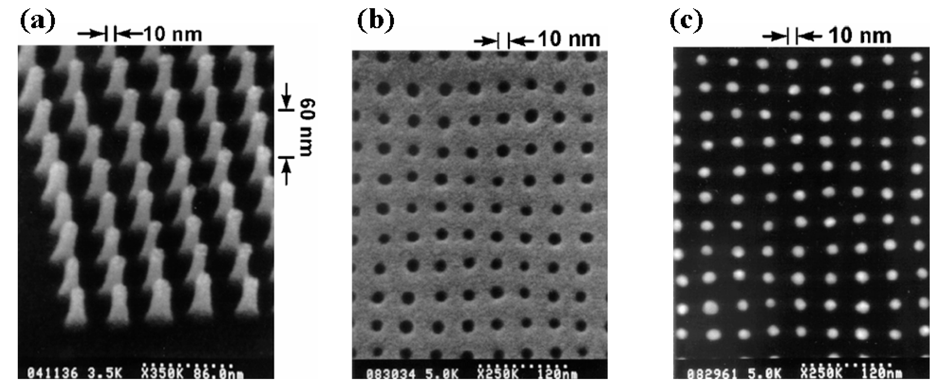
Figure 1. Micrographs showing the basic steps of NIL, demonstrated by S.Y. Chou. (a) NIL stamp in silicon with a 40 nm period array of pillars 60 nm in height, (b) imprinted 10 nm diameter holes in thin polymer film (PMMA), and (c) 10 nm metal dots after pattern transfer (lift-off), using thin polymer layer as a mask. Reprinted with permission from ref. [9]. Copyright 1997 American Vacuum Society.
Encyclopedia 05 00197 g001
Figure 2. Schematic of NIL processes involving the main steps, origination (including tooling), replication (imprint), and pattern transfer, and sub-categories such as large-area, S&R, and R2R imprint. The processes sequence is like that in photolithography (mask making, exposure, wet development, and pattern transfer). Adapted with permission from ref. [21]. Copyright 2014 SPIE.
Encyclopedia 05 00197 g002
Figure 3. NIL process chain for pattern transfer processes and device requirements. Reprinted with permission from ref. [21]. Copyright 2014 SPIE.
Encyclopedia 05 00197 g003
Figure 4. Large-area stamp and imprinted substrate, imprinted with an EVG 620HE thermal at CEA-LETI (Grenoble, France, https://www.cea.fr/ (accessed on 7 July 2025)) Cleanroom. Printed with permission. © 2012 CEA-LETI.
Encyclopedia 05 00197 g004
Figure 5. Machines and setups for NIL displaying hard and soft tool concepts. Adapted with permission from ref. [2]. Copyright 2008 American Vacuum Society.
Encyclopedia 05 00197 g005
Figure 6. SFIL process by Molecular Imprints Canon Nanotechnologies, including insert of scanning electron micrograph of resist pattern. The liquid resist (green) is imprinted after dispensing it onto a transfer layer (blue), then exposing and curing it, thinning it down (breakthrough etch), and etching it into the transfer layer that is used as a masking layer for pattern transfer into the substrate (gray). Adapted with permission from ref. [26]. Copyright 2014 American Vacuum Society.
Encyclopedia 05 00197 g006
Figure 7. Historical resist fill data along with two methods to improve throughput beyond 100 wph. Adapted with permission from ref. [52]. Copyright 2024 Yamakawa et al.
Encyclopedia 05 00197 g007
Figure 8. Potential applications, as seen by Canon, which present examples of microchip fabrication (“More Moore”) or expand to NIL applications outside the microchip domain (“More than Moore”). The schematic shows a variety of surface patterns, potential devices and application fields. Reprinted with permission from ref. [52]. Copyright 2024 Yamakawa et al.
Encyclopedia 05 00197 g008
Disclaimer/Publisher’s Note: The statements, opinions and data contained in all publications are solely those of the individual author(s) and contributor(s) and not of MDPI and/or the editor(s). MDPI and/or the editor(s) disclaim responsibility for any injury to people or property resulting from any ideas, methods, instructions or products referred to in the content.