1. Introduction
A diamond-based quantum sensor with nitrogen-vacancy (NV) centers consists of only a few key ingredients: a green light source, the diamond sample, a color filter and a photodetector. With these ingredients quenching can be performed, which is measuring the dropping fluorescence intensity in the presence of a magnetic field. Such setups are often referred to as “all optical” or “microwave-free” [
1].
To perform optically detected magnetic resonance (ODMR), which fully makes use of the advantages of a quantum sensor, additional microwave excitation is needed. Hence, a microwave generator and a microwave structure close to the diamond sample are required.
Quantum sensors and their inherent measurement principle are very interesting from a metrological perspective, since they are based on fundamental constants. In the case of the NV center, it is Planck’s constant h. This makes the measurement principle inherently drift-free and therefore calibration-free and furthermore allows for operation of such a system from cryogenic to ambient and even elevated temperatures. These advantages can be taken into account for a new generation of magnetic field sensors that can be used in areas where periodic calibration is too complex, e.g., due to poor access or similar reasons. To make these sensors accessible for industrial applications more research on compact and cost-efficient builds and their individual components is necessary. Therefore, a novel microwave resonator design that is integrated into a compact NV-magnetometer, which is referred to as the π-Mk1 platform, is introduced.
The microwave, as can be seen in energy level schemes in other publications [
2,
3,
4], increases the probability of the electron spin states of the NV center to be present in the m
s = ±1 state instead of the m
s = 0 state, if the frequency is on resonance. This in turn increases the probability that the excited electrons perform intersystem crossing (ISC), which means they do not emit red fluorescent light and therefore a dip in the ODMR spectrum can be observed. Further detailed information on the working principle of NV centers in diamonds can be found in [
5]. However, there can be up to four dip pairs in the ODMR spectrum corresponding to the four axes of an ensemble diamond. The distance of each dip pair gives a measure of the magnetic field strength parallel to the corresponding diamond axis. With all four axes, not only the absolute magnetic field strength but also its vector component can be measured.
The literature provides many different solutions for microwave excitation. The simplest forms of microwave structures are transmission lines and microstrips with impedance matching [
6,
7,
8] or coplanar waveguides [
9,
10]. They create constant magnetic fields around the length of their conductor over the whole frequency spectrum, but are inhomogeneous in the space around them, which is a disadvantage when used for quantum sensing.
Therefore, many examples use microwave structures with a circular hole, in which the diamond can be populated. These designs often use resonators containing a parallel LC-circuit, which is often referred to as an Ω-structure, in which the trace on a printed circuit board (PCB) is arranged in a way to form a capacitor and at one end of the structure a loop that serves as an inductor. In the center of the loop is a hole for the diamond, where the microwave field is partially homogeneous [
6,
11,
12,
13,
14,
15,
16,
17,
18]. There are also some variations from the classical Ω-structure, with additional coils around the structure to adapt the return loss over frequency to the needs of the application [
19].
Another way to design the microwave structure and to build a resonator is the usage of split-ring resonators [
3,
8,
13,
20,
21]. These are structures with two or three coupled rings. Every ring is interrupted at a certain position to form a capacitor, while the rest of the ring forms the inductor.
Further approaches use a microwave circuit with polarization- and frequency-tunable components [
22], a hole-and-slot type loop gap resonator to provide three-dimensional homogeneous fields [
23], a coil- and wire-based microwave setup [
18], a compact annular ring microstrip antenna (although this approach has not yet been used for NV-based quantum sensing) [
24], different shapes of lumped resonators in combination with a microwave planar ring antenna [
25] and an LC-circuit built from discrete components, e.g., a 1 pF capacitor and a wire loop with a diameter of 2 mm [
26].
Most of the mentioned microwave structures are built on rigid PCBs, which makes them bulky and not suitable to be integrated in a small sensor head; some of them are directly applied to the diamond. Nevertheless, Deguchi et al. [
27] used a microwave resonator with a λ/4 transformer built with copper foil on a polyimide sheet and attached copper wires for a pair of λ/4 open stubs. However, this structure can only provide a weak microwave field.
Most of the introduced microwave structures from the literature require space, and were fabricated using advanced technologies such as physical vapor deposition (PVD) or were handcrafted. None of them, however, fulfilled the needs of this study, that is, being easy to fabricate at low cost in large quantities, having high reproducibility and being mechanically flexible to be bent and fit into a limited amount of space, while at the same time providing a strong microwave field with a minimum of microwave power. Hence, this work used a standard two-layer flexible printed circuit board stack with a double-sided 18 µm copper layer and a 25 µm polyimide core, available at almost any PCB manufacturer, to serve as the basis for a resonator. To prevent the use of ferromagnetic materials, an immersion silver surface finish was selected over Electroless Nickel, Immersion Gold (ENIG). The purpose of this work was to design the resonator in such a manner that it fits into the π-Mk1 platform and fulfills all criteria in combination with this platform to produce CW-ODMR spectra.
2. Materials and Methods
The objective was to provide a resonant structure that creates a strong microwave field with as little microwave power as possible that then couples into NV centers in a diamond to excite their ms = ±1 states. The resonance frequency of the structure should be centered around 2.87 GHz with a bandwidth of at least 300 MHz. For reproducible mass-manufacturing of such a structure, a stack of a 2-layer flexible printed circuit board (FPC) with 25 µm polyimide core, double-sided 18 µm copper layers and immersion silver surface finish was chosen. The impedance should match 50 Ω with a power handling of up to +30 dBm. The dielectric constant of polyimide is 3.3 and the loss factor 0.02. For a low-profile electrical connection, a U.FL connector was selected.
To design and optimize the structure, a design and simulation chain consisting of the open source software KiCad (version 9.0.0), FreeCad (version 1.0.0) and openEMS (version 0.0.36) was applied. Several optimization runs were performed to obtain a microwave structure with the above-mentioned properties.
Prototypes of the resonators were fabricated in-house using roll lamination of a dry resist film on both sides of a copper-cladded polyimide substrate, direct imaging, wet development, and wet etching, and finally the resist masking was removed with acetone.
After prototyping the simulated microwave structures, the return loss S11 was measured by a vector network analyzer, ZNLE6 (VNA, Rohde&Schwarz, Munich, Germany), supplied by a 10 MHz reference clock provided by a Trimble Thunderbolt E (Trimble, Sunnyvale, CA, USA) global positioning system disciplined oscillator (GPSDO).
To show that the microwave structure approach is appropriate for NV-based magnetometers, the structure was then integrated into the so-called π-Mk1 platform, which is a similar but further miniaturized NV-magnetometer setup compared to the one shown in the authors’ previous publication [
26]. This time a PCB as the basis of the sensor head was used and all critical components were arranged laterally in the PCB. Amplification and a constant current source were assembled on the PCB. LED3 from [
26], the diamond MDNV700850um50mg (Adámas Nanotechnologies, Raleigh, NC, USA), the color filter LEE 027 MEDIUM RED (LEE Filters Worldwide, Hampshire, UK) and the photodiode BPW34 (Vishay, Malvern, PA, USA) were used.
As a microwave generator, ADF4351 evaluation boards were used. The first board (board 1) was used with no modifications, which means the board has a differential output of which one is used while the other is terminated with a 50 Ω resistor and the output power can be set to –4, –1, +2 or +5 dBm. The second board (board 2) was modified according to the datasheet with an LC balun to convert the differential output into a single-ended output similar to [
26]. This board can be set to output powers of –1, +2, +5 or +8 dBm. An STM32 microcontroller (µC) controls the ADF4351 board through an SPI interface. The µC itself is controlled by a personal computer through a USB interface with a mathematical program (GNU Octave, version 9.3.0 (12 December 2024)). To perform CW-ODMR measurements a microwave frequency sweep is performed between 2.67 and 3.07 GHz with 801 steps. The photocurrent of the photodiode is converted into a voltage by a transimpedance amplifier (TIA) with a bandwidth of ~200 Hz. Its output voltage is then sampled with an oscilloscope (MSO46-4-BW-1000, Tektronix GmbH, Köln, Germany) with a sample rate of 125 kS/s. Additionally, the µC provides a trigger signal for the oscilloscope, indicating the start of a new sweep. An average signal of 16 consecutive CW-ODMR spectra was saved as a data file and post-processed on a personal computer with GNU Octave. The π-Mk1 platform was powered by a USB-based low-noise power supply, which makes use of a DC-DC-converter followed by low-noise linear dropout regulators (LDOs) with appropriate filtering in the different sections of the circuit.
3. Results
3.1. Simulation Results of Resonator
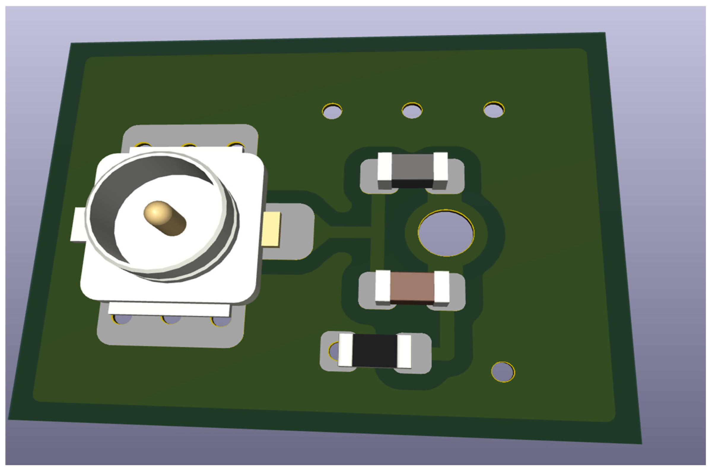
First, an approach using lumped components to create an LC parallel resonant circuit and a via to get the current to flow into the via and radiate into the diamond structure was simulated (
Figure 1). This failed to give good yield, mainly due to the very thin stack-up, resulting in large losses due to the lumped components’ footprint size (0402 imp) and poor matching due to too-low mating impedance.
Next, a pure microwave structure, inspired by the results presented in [
27], was designed. In this, a λ/4 transformer on polyimide foil was combined with λ/4 open stubs made from two copper wires.
In the original design from [
27], open-air λ/4 stubs were employed to achieve the last impedance transformation, which ends up at 50 Ω at the input. However, this configuration inherently lacks a defined return path and exhibits a low radiation impedance, causing the network to behave primarily as a mismatched transformer rather than a radiating element. Evidence of this mismatch can be observed in the Smith chart measurement in the referenced publication, which never reaches the 50 Ω reference point, indicating persistent reactive loading rather than true impedance matching. Consequently, the stubs only contribute some capacitance loading and produce strong reflections at the λ/4 connections, undermining efficiency as the field coupled into the diamond mainly comes from the open unterminated end of the first λ/4 transformer and only one edge of the diamond is subjected to the RF microwave field.
To overcome these limitations, a two-part resonator design on an FPC substrate was implemented. First, a U.FL connector is placed and is matched into true 50 Ω by means of a small microstrip inductor that then feeds a 22 Ω λ/4 microstrip line, acting as a λ/4 transformer that steps down the impedance from 50 Ω input to around 8 Ω output, significantly boosting current density. Next, this microstrip line connects to two λ/4 open-ended stubs, carefully impedance matched to form a resonant termination. This design creates a voltage maximum at the stub ends and a current maximum at their junction.
Initial simulations with a solid ground plane showed that while current density at the entry was high, it remained confined between the thin dielectric layers, resulting in very little radiation into the intended diamond coupling region. To address this, a deliberate slit in the ground plane was introduced and a conductive via at the coupling position placed, forcing the return current path through the via structure and the concentrating current into the via in which the diamond is placed.
This modification introduced two potential issues:
The via and slit in the ground plane caused impedance discontinuities, creating reflections and limiting power transfer into the stubs.
A secondary resonance appeared in the ground plane, risking cancellation of the desired resonant current.
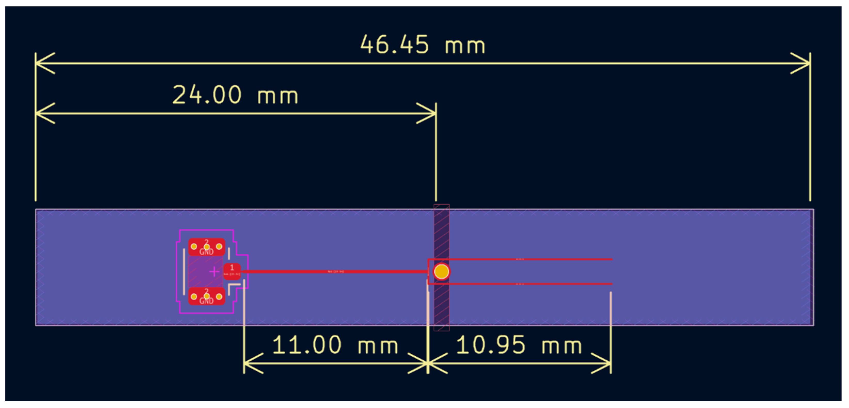
To reduce these issues, the ground plane was enlarged beyond the top structure dimensions, lowering the secondary resonance effect and effectively improving the overall bandwidth of the resonator structure (see
Figure 2 and
Figure 3).
Ultimately, this design approach significantly enhances uniform coupling of microwave fields into the diamond compared to previous methods.
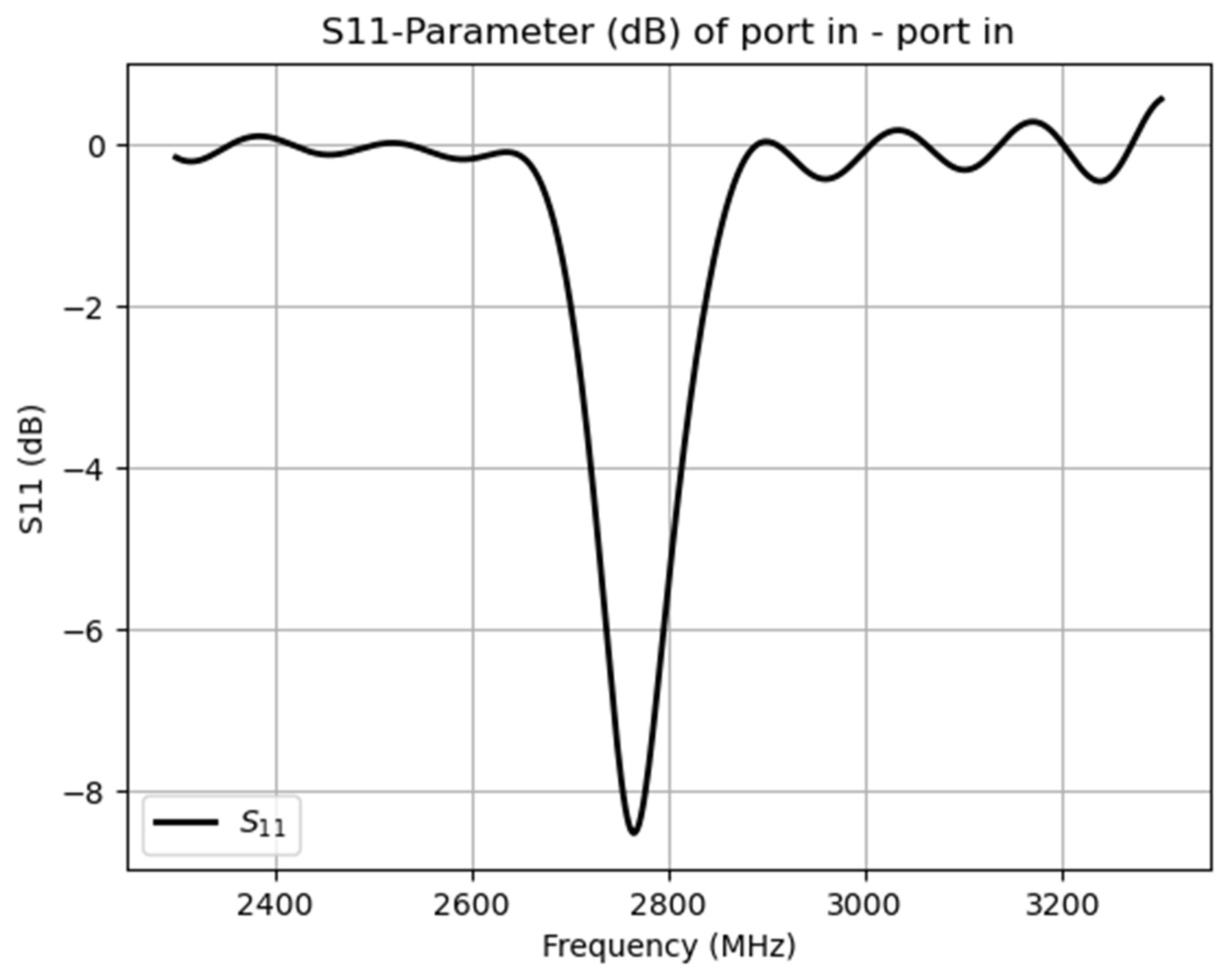
The final design was simulated with the help of FreeCAD and openEMS EM solver. The lengths of the structure were tweaked and the current field in the center of the via was observed. The final simulation was stopped when the resonance was slightly below the ideal operating frequency (
Figure 4).
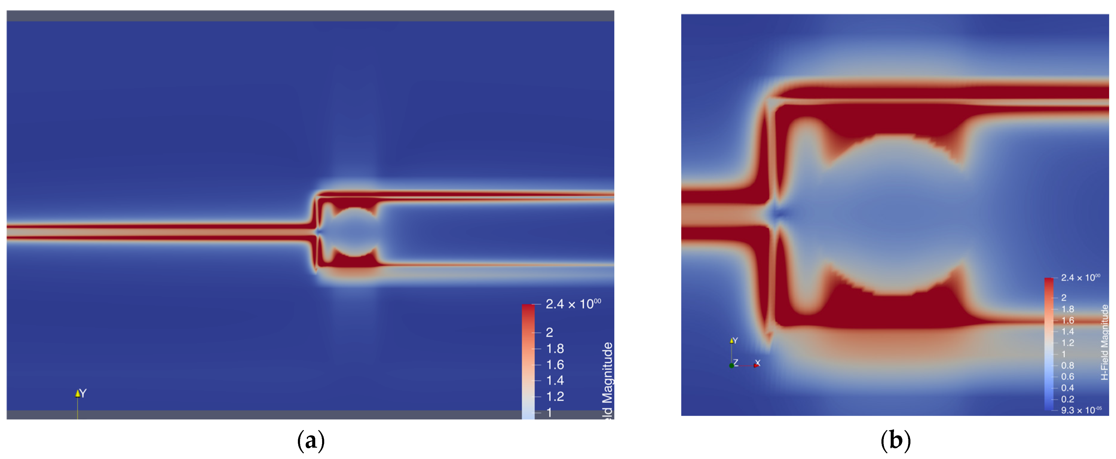
This was performed to leave room for tweaking after prototypes were made as it is hard to reliably predict exact material parameters with such thin stack-up and it is much easier to trim the length of the traces with a scalpel, while the ground plane can be trimmed by simply cutting each end with scissors. Using the simulation shown in
Figure 5 the goal of concentrating the current inside the via hole for the diamond was achieved.
The S11 is not very low, but this is partly due to the limited time step in the simulation to dissipate all the power (performed due to simulation time). On the final prototype this was expected to be both lower and with more distinct difference between the two resonant modes.
One interesting aspect of this design is how efficiently it drives the current into the loop, even when the S11 is very far off from the main resonance. Although most of the power is reflected back towards the input, that reflection actually occurs at the stub ends rather than at the input connector. These end reflections travel back into the loop and effectively double its current over a wide frequency range.
This doubling persists until the excitation frequency becomes high enough for a λ/2 condition or low enough for a λ/8 condition. At these points, the forward and reflected currents cancel and the loop current falls down to zero. However, the further one moves away from the ideal λ/4 match, the more the phase between voltage and current shifts, so the current density gradually decreases above and below the center frequency.
3.2. Resonator Prototyping
The first prototype samples of the resonator design were manufactured in-house using the aforementioned FPC stack by roll lamination of a 50 µm dry resist film (Ordyl FP 450, Elga Europe, Nerviano (MI), Italy) onto both sides of the copper cladding, direct imaging using 365 nm UV light (DI 2020L, MIVA Technologies, Schönaich, Germany) and wet development in potassium carbonate (K
2CO
3) developer to finalize the masking process. The copper cladding was wet etched by ammoniacal etching (Etching Center S30HS, Walter Lemmen, Kreuzwertheim, Germany). Finally, the resist masking was cleaned off by acetone (
Figure 6). The via in the prototype was realized by drilling a hole and covering the walls of the hole with silver ink.
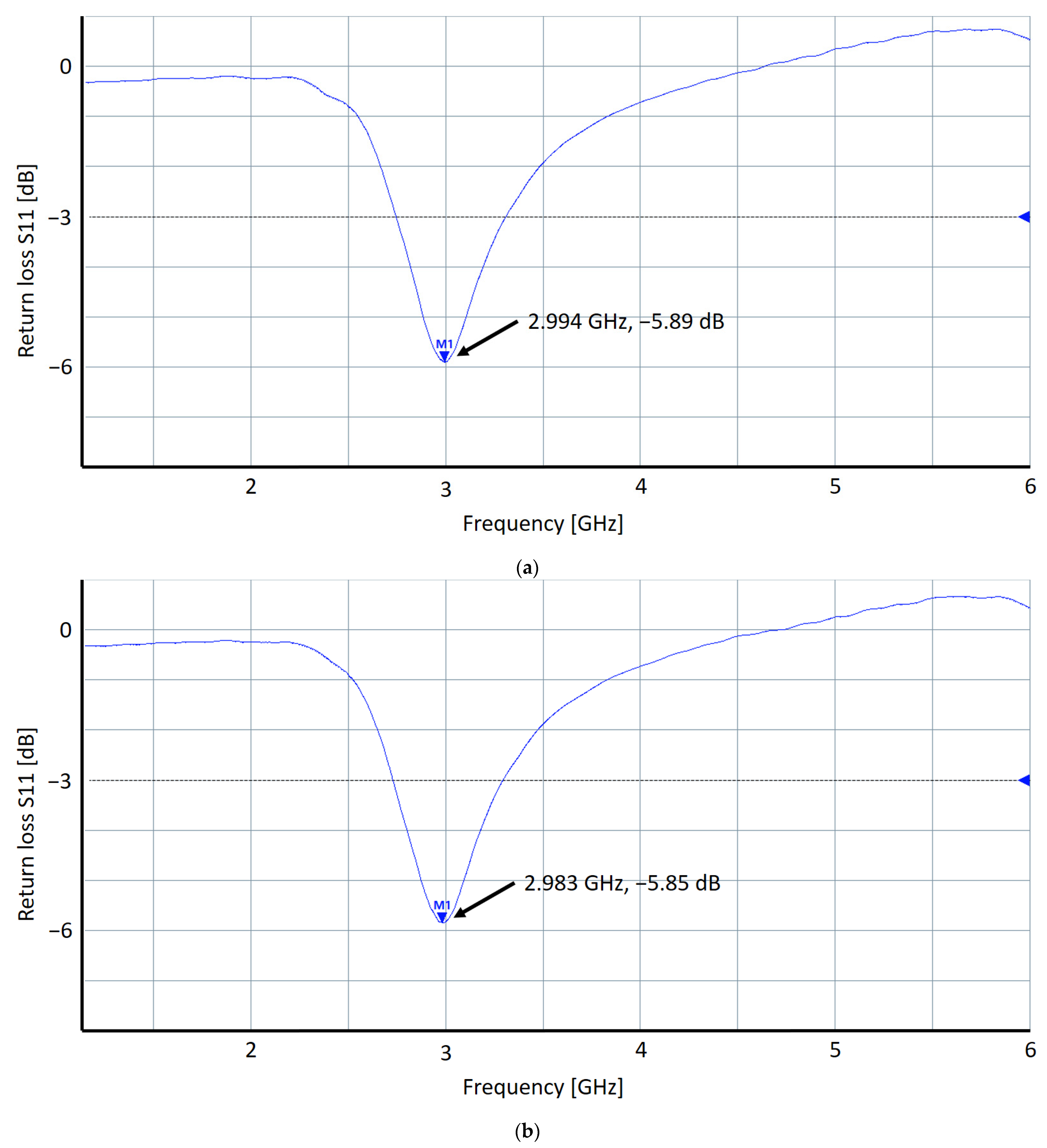
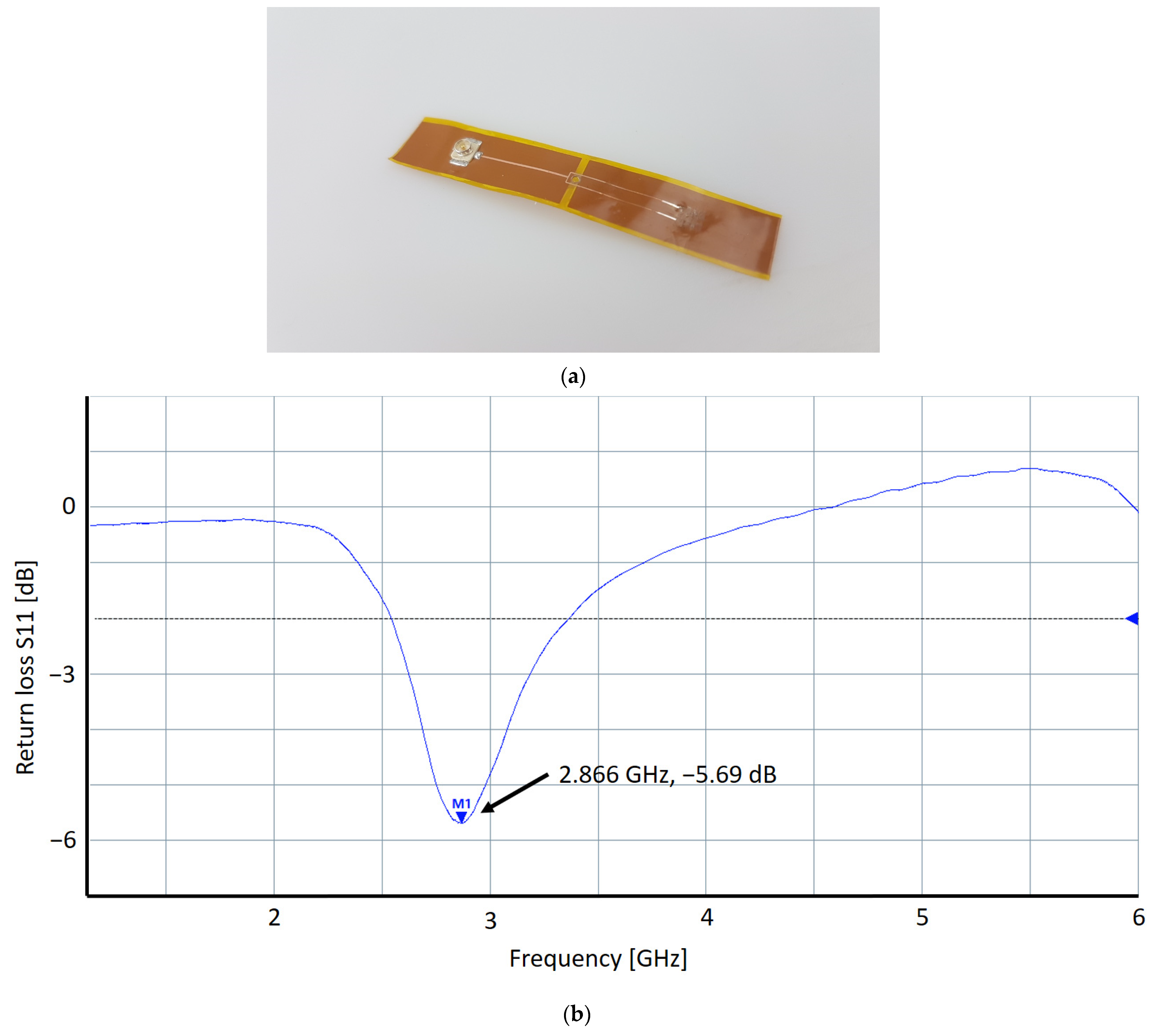
These samples were then characterized (
Figure 7) using a vector network analyzer, ZNLE6 (VNA, Rohde&Schwarz, Munich, Germany), supplied by a 10 MHz reference clock provided by a Trimble Thunderbolt E (Trimble, Sunnyvale, CA, USA) global positioning system disciplined oscillator (GPSDO).
The first step attempted to optimize was reducing the length of the longer of the two ground planes in order to shift the resonance closer to the main λ/4 structure resonance, to broaden and lower the total resonance, which should result in a larger bandwidth.
Figure 7a shows the return loss before and
Figure 7b that after trimming of the ground plane.
However, this did not change the resonance at all, hence why the length of the open stubs was improved next by extending them with silver ink and trimming them in length until the requested result, a resonance frequency close to 2.87 GHz, was achieved by VNA measurements.
Figure 8a shows the resonator with improved stub length and
Figure 8b the corresponding return loss measurement.
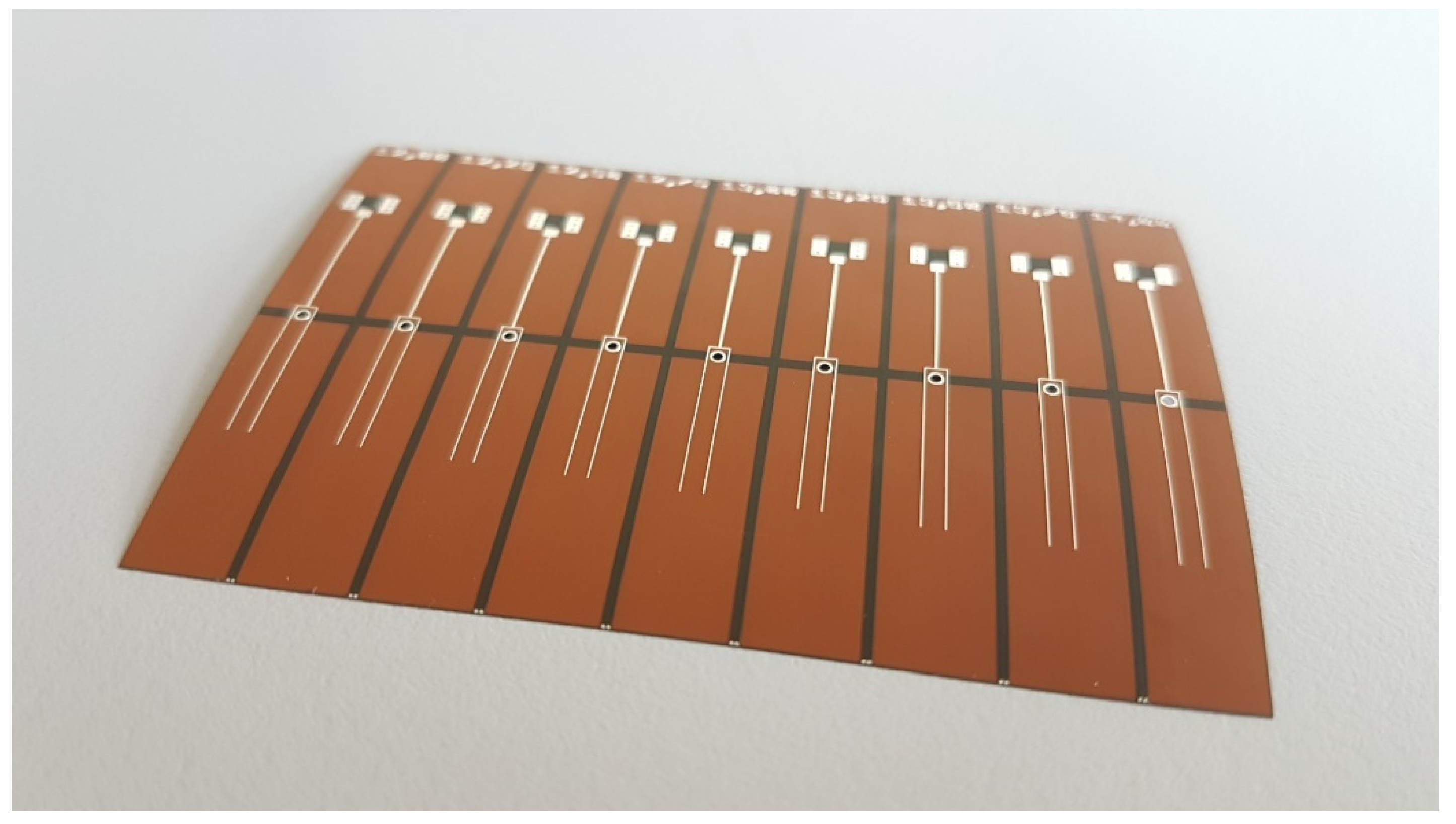
The optimal stub length was found to be 12.25 mm for this sample. Based on these findings, a panel with several different stub lengths ranging from 12.00 mm to 14.00 mm in steps of 0.25 mm was ordered from a PCB manufacturer (
Figure 9), since the final stack parameters could differ between various PCB houses. Immersion silver for surface finish and a black cover layer for the bottom were chosen. These panels were again characterized with a VNA.
The resonators were separated from the panel, fitted with U.FL connectors and characterized. It was found that, again, resonators with a stub length of ~12.25 mm perfectly matched the previous results for the prototype sample. Within a quantity of 16 samples, the average resonance frequency was measured to be 2.856 ± 0.031 GHz, while the average S11 was measured to be −5.005 ± 0.267 dB. The deviation in resonance frequency between samples appears to be larger than expected; however, it can be blamed on the RG316 cable used for the measurements, which might be insufficient to provide reproducible and phase-stable results at these frequencies. Nevertheless, even with a resonance frequency of 2.87 GHz this resonator can achieve strong microwave excitation due to its large bandwidth and the concept that the current running through the via creates a microwave field for exciting the NVs.
3.3. Integration of Resonator to Perform CW-ODMR in an NV-Based Magnetometer
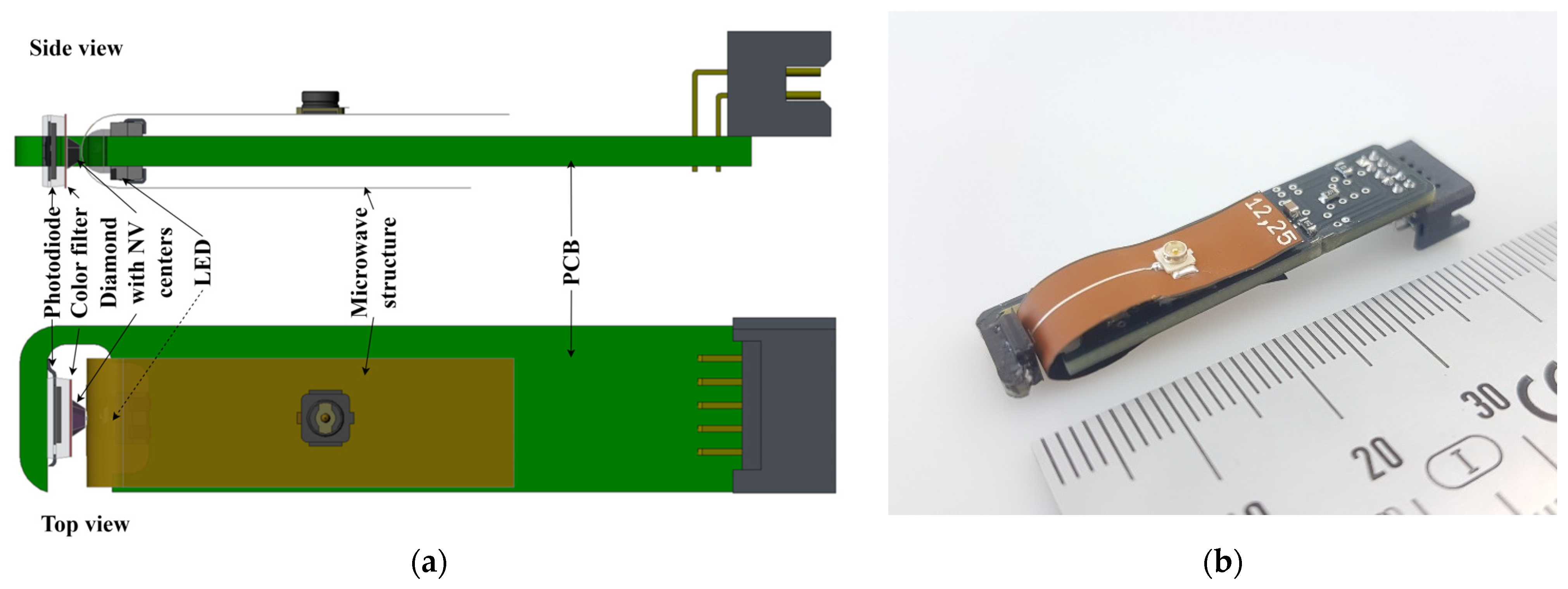
Finally, the resonator was integrated into the π-Mk1 platform to excite nitrogen-vacancy centers in a diamond sample. The platform consists of an LED, a diamond containing NV centers, a color filter and a photodiode. All the optical components are laterally integrated into a printed circuit board, which features a PCB-based spring to compensate for thermal expansion. Additionally, the board contains a constant current source, a transimpedance amplifier, optional offset compensation and an output boost stage. It measures 9 mm × 40 mm, which results, together with its case, in a volume of π cm3, hence the name. The resonator is folded around the LED, with the diamond sample sitting inside the via of the resonator.
Figure 10a shows a drawing of the basic PCB of the π-Mk1 platform with its optical components and the way the resonator is integrated into it.
Figure 10b shows the built π-Mk1 platform and its size.
The π-Mk1 platform was connected to the microwave generator boards 1 and 2 consecutively, the µC, the oscilloscope and the power supply to perform CW-ODMR measurements.
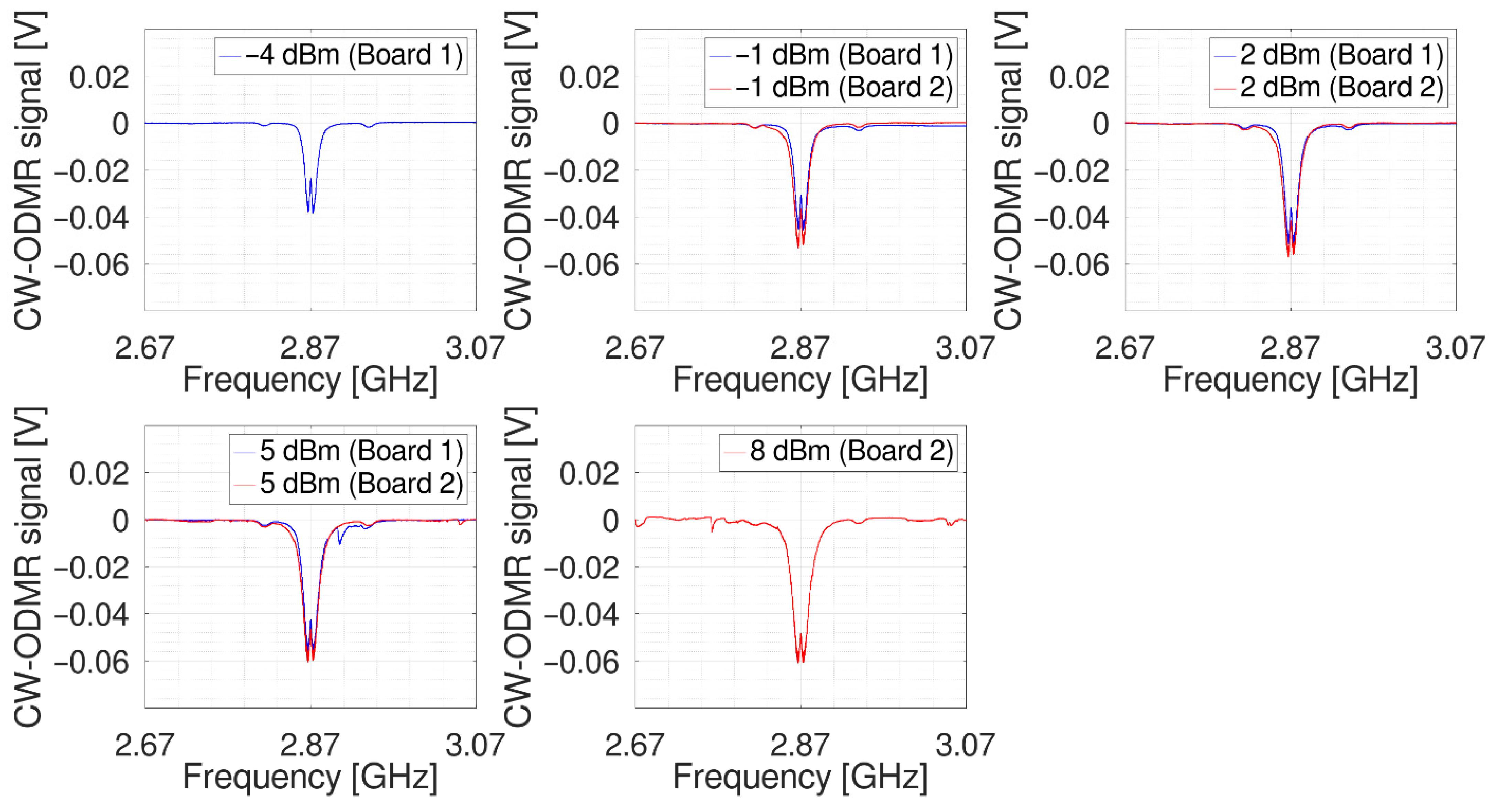
The first CW-ODMR signals were conducted without any additional magnetic field at different microwave powers for each microwave generator board.
Figure 11 shows the results for board 1 with blue-colored lines and those for board 2 with red-colored lines. The curves show the zero-field-splitting (ZFS) for the used diamond sample at 2.87 GHz as expected. The dip height at resonance frequency increases with increasing microwave power. On each side of the resonance dip, smaller dips, asymmetrical to 2.87 GHz, can be found that reveal
13C interaction. Measurements with the different boards show slightly different curve progression at some frequency positions and different dip heights. CW-ODMR signals with microwave powers of −4, −1 and +2 dBm appear to be smoother. However, for higher microwave powers, power broadening and sidebands show up, leading to a distorted ODMR spectrum as reported in [
28].
In a second series of measurements with the same setup, a permanent ring magnet was placed at the central lateral axis of the NV-magnetometer. The magnetic field at the measured position was ~5 mT in the lateral direction and almost 0 in the direction of the other two spatial axes. This was measured with a 3D Hall sensor evaluation kit (TLE493D-P2B6 MS2GO, Infineon, Neubiberg, Germany). The results for this applied external magnetic field are shown in
Figure 12. Two of the maximum four dip pairs are visible in this position of the magnetic field in relation to the diamond sample in the π-Mk1 platform, which can be explained by the HPHT diamond being oriented with its 111 axis towards the photodetector and thus parallel to the magnetic field lines of the ring magnet. With an external magnetic field, CW-ODMR signals only show a smooth progression for −4 dBm. At higher microwave powers, power broadening and sidebands show up and lead to distortions in the ODMR spectrum. These sidebands are partially bandwidth-limited by the TIA.
4. Discussion
While simulations of the stub length resulted in a value of 10.95 mm (
Figure 2), real-world measurements revealed an optimal length of 12.25 mm (
Figure 8). This is most likely due to the assumed velocity factor in the FPC material, which differs in reality. However, increasing the stub lengths using silver ink on the first prototype samples and trimming their length resulted in an optimum of 12.25 mm to achieve a resonance frequency of ~2.87 GHz. Nevertheless, a panel with a variety of different stub lengths was ordered. The previously found result was reproduced and resonators with a stub length of 12.25 mm performed similarly. This shows that good reproducibility in resonance frequency and S11 can be achieved with this resonator on the FPC stack chosen. Copper etching accuracy today is remarkably good, since manufacturers often compensate for over-etching of thin traces. This is why for PCBs errors should not be more than 0.1 mm. This would then cause a shift so small that it is almost impossible to measure. The thickness tolerance is 10%, and also, here, while it could be measured, the end result would be expected to be on the noise floor. The thickness would affect the impedance more than the velocity factor, while velocity factor vs. thickness is attenuated. Changes in the substrate itself could result in a frequency shift, but since polyimide was used for the substrate, this is highly unlikely. On FR4, however, it can quite often be seen if there are changes or shifts in the fiberglass weave pattern.
Preliminary measurements in the NV diamond quantum setup finally revealed that the microwave power had to be decreased from the former value of +5 dBm [
26] down to −1 dBm and below in order to prevent sidebands of the ODMR spectrum as reported in [
28]. However, at −4 dBm, which is the minimum power the ADF4351 can be set to, which is a wideband synthesizer with an integrated voltage-controlled oscillator, ODMR spectra that are still strong and clean, as shown in
Figure 11 and
Figure 12, can be observed. This proves the concept of the design, in which a strong microwave field is created within the via of the resonator.
Table 1 compares the resonator used in this work to reported microwave structures in terms of their size and the microwave power they were operated at. The microwave power used in this work appears to be the lowest on the list. However, the lower microwave power limit at which ODMR for the resonator in this work can still be observed needs to be evaluated in future work. Furthermore, this study should also be combined with varying optical excitation power, since this could lead to similar effects like power broadening due to NV spin saturation.
Nevertheless, observations of the presented results are in accordance with [
28], where the dip height of the CW-ODMR signal also increases with increasing microwave power, more side resonances occur in the presence of a magnetic field and the occurrence of
13C interaction is observed.
Table 2 compares different LED-powered magnetometers by their physical size and power consumption. This, however, is not a fair comparison due to different levels of integration, because the magnetometer built in [
3] incorporates only an LED without a lens, the resonator and a photodiode, while signal detection was realized using an external lock-in amplifier and external vector signal generator. The magnetometer built in [
7] includes a TIA and a constant current source for driving the LED, which itself does not contain a lens, and the setup uses an external 14-bit sampler and an external microwave source. The magnetometer in this work also uses an integrated TIA and constant current source for driving the LED with a lens, so it is more similar to [
7]. It drives the LED with ~100 mW of electrical power and the resonator with −4 dBm (~400 µW). The rest of the power (~120 mW) is used in the constant current source and for the TIA. However, the sensitivity achieved with the build in this work is as yet unknown and needs to be measured in the future.
To bring quantum sensors into industrial applications, further research is necessary on small, power- and cost-efficient sensors. The demonstrated microwave structure is an example of a low-cost, low-power, reproducible and mechanically flexible design that seamlessly fits into the small space of the miniaturized quantum sensor. The presented π-Mk1 platform also serves as an example for low-cost NV-based magnetometers. Such approaches are necessary to bring quantum sensing into industrial applications and make use of their inherently drift- and calibration-free measurement principle. More detailed measurements and characterization of the π-Mk1 platform in combination with the microwave structure presented here are planned to be published in an upcoming publication.
Although designed for a resonance frequency of 2.87 GHz and as an FPC for room-temperature operation to excite NV centers in diamond samples within the π-Mk1 platform, the overall design approach is not limited to this. Instead, the design can be adapted to other frequencies and other board stacks with different substrate materials, such as FR4, PTFE, PEEK, ceramic, glass, sapphire, etc., and can even be applied to excite samples operated at cryogenic temperatures, such as 2,2′-dinaphthylcarbene (DNC) embedded in a structurally related crystalline 2,2′-dinaphthylketone (DNK) matrix [
29] and others. In this case the coefficient of thermal expansion has to be taken into account and the resonator needs to be designed to match the requirements at operational temperature.
