Article

Ultra-Small Temperature Sensing Units with Fitting Functions for Accurate Thermal Management

Department of Electrical and Computer Engineering, Iowa State University, Ames, IA 50011, USA
*
Author to whom correspondence should be addressed.
Metrology 2025, 5(3), 46; https://doi.org/10.3390/metrology5030046
Submission received: 15 May 2025 / Revised: 18 July 2025 / Accepted: 22 July 2025 / Published: 1 August 2025

Abstract

Thermal management is an area of study in electronics focused on managing temperature to improve reliability and efficiency. When temperatures are too high, cooling systems are activated to prevent overheating, which can lead to reliability issues. To monitor the temperatures, sensors are often placed on-chip near hotspot locations. These sensors should be very small to allow them to be placed among compact, high-activity circuits. Often, they are connected to a central control circuit located far away from the hot spot locations where more area is available. This paper proposes sensing units for a novel temperature sensing architecture in the TSMC 180 nm process. This architecture functions by approximating the current through the sensing unit at a reference voltage, which is used to approximate the temperature in the digital back end using fitting functions. Sensing units are selected based on how well its temperature–current relationship can be modeled, sensing unit area, and power consumption. Many sensing units will be experimented with at different reference voltages. These temperature–current curves will be modeled with various fitting functions. The sensing unit selected is a diode-connected p-type MOSFET (Metal Oxide Semiconductor Field Effect Transistor) with a size of W = 400 nm, L = 180 nm. This sensing unit is exceptionally small compared to existing work because it does not rely on multiple devices at the sensing unit location to generate a PTAT or IPTAT signal like most work in this area. The temperature–current relationship of this device can also be modeled using a 2nd order polynomial, requiring a minimal number of trim temperatures. Its temperature error is small, and the power consumption is low. The range of currents for this sensing unit could be reasonably made on an IDAC.

1. Introduction

Temperature sensors are frequently built on-chip for many different applications. One of these applications is IC thermal management. Thermal management is focused on dissipating heat from integrated circuits to reduce negative temperature effects. High temperatures will speed up the aging process, reducing an IC’s lifespan [1]. Locations where power is being dissipated will have higher temperatures as electrical energy is converted to thermal energy. Many temperature sensors are placed on-chip at these locations [2,3]. If the on-chip temperature surpasses a certain threshold, cooling technologies like fan forced convection and water cooling can be used to reduce the chip’s temperature. The device may also shut down to reduce thermal energy dissipation.
Many architectures have been proposed for on-chip thermal management temperature sensors. Most rely on generating either proportional to absolute temperature (PTAT) signals or complementary to absolute temperature (CTAT) signals at the temperature measurement location [4,5,6,7]. Once this signal is generated, it is quantized using an analog to digital converter (ADC) and the temperature is calculated using a linear relationship in the digital domain. Temperature sensors using this architecture will typically have one ADC on each chip and use switches to measure each temperature sensors’ signal independently. A block diagram of this common architecture is shown in Figure 1.
The area to generate the PTAT and CTAT signals is large, limiting the number of temperature sensors that can be made and where they can be placed [3]. The ADC also consumes significant area, reducing area available to other circuit components.
Other existing architectures generate temperature-dependent voltages from individual devices by using a current source connected to the device [8,9]. Once the voltage is generated the temperature can be predicted using known temperature-dependent equations and data analytics techniques. While this reduces the size of the sensing unit, an ADC is still needed to convert to the digital domain if the temperature is going to be stored in memory.
One motivation for this research is to minimize the size of the sensing unit. As mentioned, many architectures for temperature sensors in thermal management use a central control circuit with many sensing units. These sensing units are located near high-activity circuits where high temperatures are measured. These circuits often have very compact layouts, so there is little room for sensing units or full temperature sensor implementations. Due to the steep temperature gradients that are created from these circuits, it is also necessary that the sensing units be located very close to these circuits [3]. It is essential to reduce the size of the sensing units so that the temperature can be measured among compact circuits.
Another motivation for research in this area is accurate temperature measurement [10,11,12,13]. When temperature measurements are too high, cooling technologies are activated prematurely, degrading system performance. When temperature measurements are too low, cooling technologies are not activated, which leads to reliability issues. Accurate temperature readings are critical for thermal management temperature sensors, because high accuracy is critical for the performance and reliability of their systems.

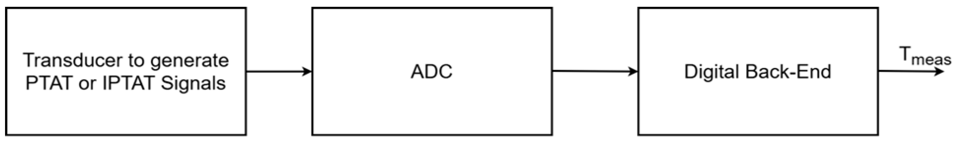
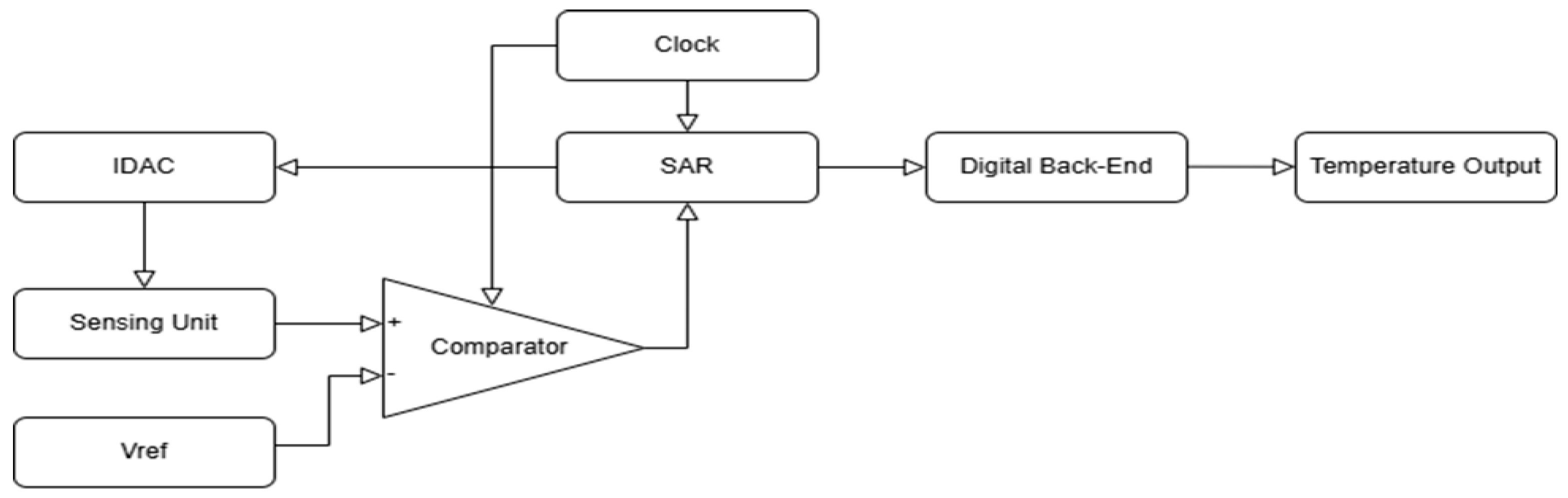
2. Proposed Architecture

The architecture proposed in this work aims to resolve some issues with existing temperature sensors used for thermal management. A block diagram of the proposed architecture is shown in Figure 2.
This architecture will use a successive approximation register (SAR), current steering digital-to-analog converter (IDAC), and comparator in the central control circuit to approximate the current through a sensing unit at a given reference voltage. This SAR will update the current sourced by the IDAC through an iterative process. The goal of this process is to make the voltage on the sensing unit as close to the reference voltage as possible. When the voltage on the sensing unit is lower than the reference voltage, the current will increase in the next step of the iteration. The opposite is also true. When the iterations are complete, the digital current code is sent to the digital back-end and the process is repeated. Only the sensing unit will be at the temperature measurement location. Once the temperature-dependent current is quantized, the temperature will be approximated from the current in the digital back end using fitting functions. If switch arrays are used, then many sensing units can be placed on a chip with only one control circuit. One sensing unit can be connected to the control circuit at a time to sense the local temperature.
This architecture aims to resolve many of the issues present in existing thermal management temperature sensors. One of these issues is sensing unit size. Most existing architectures rely on using multiple devices at the temperature measurement location, while this architecture uses only one. Consequently, the sensing unit can be closer to the desired temperature measurement location. The sensing unit can also be made arbitrarily small if its temperature–current relationship can be modeled using fitting functions.
This architecture can also address path size to the sensing unit. Many existing architectures function in the voltage domain. Consequently, wide paths are used to reduce the resistance between the DAC and the sensing unit [3]. In some cases, sensing units cannot be placed because they are far from the central control circuit. In this architecture, the current domain is used, which would allow reduced path size and sensing units to be placed far from the central control circuit. The effects of the voltage drop along the lines can be neglected by using a double differential comparator. The differential input can come directly from the sensing unit, eliminating voltage drop along the paths. If the resistance from the paths does not push headroom specifications from the IDAC, the paths can be made arbitrarily small. In summary, path size will be addressed by this architecture, allowing the sensing units to be placed in compact locations and reducing area consumed by paths.
Most existing architectures use voltage-mode ADCs to quantize the PTAT and CTAT signals. Because this architecture goes directly to the digital domain, area does not need to be budgeted for a voltage mode ADC. However, area will need to be budgeted for the IDAC, comparator, SAR, and reference voltage generator for quantization.
The last advantage of this architecture is fitting functions. Many architectures that generate PTAT and CTAT signals require calibration temperatures even when the generated signal has a known linear temperature relationship. If calibration temperatures are already being used, generating the PTAT and CTAT signals may not be necessary. The temperature–current relationship can be modeled using fitting functions, which opens the door to data analytics techniques and machine learning, making the possibilities for this architecture endless.
There are some specifications and goals for this architecture. First, reducing the size of the sensing unit will be a primary focus to allow the temperature measurement to be close to the high-activity circuits. A temperature range of −40 to 125 °C will be used for this research. This temperature range is close to temperature ranges used in other thermal management research and is a common temperature range for industrial applications [14]. A temperature inaccuracy goal of ±0.16 °C will be used for this work. This inaccuracy goal is close to temperature inaccuracies reported in existing research. In this work, simulations will be performed instead of measurements, so the ±0.16 °C inaccuracy definition will only be generally referenced. It corresponds to a 9-bit definition across the temperature range. Throughout this paper, temperature error is also referenced to as integral non-linearity (INL). INL is the largest temperature error seen across the operating temperature range of −40 to 125 °C for a given sensing unit, reference voltage, and fitting function. Power consumption will also be considered in this research. While a specific power specification is not set, power delivered to the sensing unit should be minimized. If power for one sensing unit is reduced, more sensing units can be measured at once for a given total power specification if multiple sub-circuit components are available. Reducing power consumption will also reduce thermal gradients created by the sensing unit itself, which could distort temperature measurement results.

3. Sensing Unit and Fitting Function Design

Modeling temperature–current relationships of many different sensing units will be completed because the sensing unit and the digital back end are the most novel parts of this architecture. They introduce the approximating function error, which is a novel form of error in this architecture. Other sources of error like the quantization error have been widely studied, and their effects are well understood.

3.1. Selection Methodology

A test bench with an example sensing unit for data collection is shown in Figure 3. The instance on the left of this schematic is a DC voltage source. It is used to represent the reference voltage in the proposed architecture. The instance on the right is an example sensing unit, a diode connected n-type MOSFET. This test bench can be used to select a sensing unit to be placed in Figure 2. It can be used to model the temperature–current relationship of a device, which can then be placed into the full block diagram. The sub-circuit components in the full block diagram will introduce other sources of error, like quantization error, temperature dependencies, and local random variations introduced from the semiconductor process.
A few goals are used to guide the exploration of modeling temperature–current relationships. These goals can be derived from a three-stage design characterization. The first stage is a device with a known temperature–current relationship which is a function of the device(s) used, their dimensions, and the reference voltage(s). The power and area used in the device(s) should be minimized. The second stage is quantization. A larger current range will loosen the requirements for the IDAC by increasing the size of the LSB needed. A larger small signal input impedance to the sensing unit will also help the comparator distinguish between two adjacent IDAC outputs. Finally, the temperature–current relationship should be simple to model using a fitting function. The error from this function should be minimized and the number of parameters should be reduced to minimize test cost [15].
The parameters for generating the temperature–current relationships are the device(s) used, their dimensions, and the reference voltage(s). The modeling of temperature–current relationships will be dependent on the approximating functions used.
The following was performed after simulation to process the data before it was fitted. The difference between the currents for two devices with similar reference voltages was calculated. This new curve represents T   v s .   d I d V which would give fundamentally different results compared to the T   v s .   I curves. If this rendered good results, the currents could be quantized individually and the difference taken in the digital domain. In addition to the difference curves being added to the data sets, all temperature and current data was normalized using a min–max normalization. This means that the temperature and current values being fitted will have a range from zero to one. This was performed because the data coming from the IDAC will be normalized across the current range using digital codes and normalizing data is a common data analytics technique.

3.2. Fitting Functions

The equations chosen to model the temperature–current relationships are shown in Table 1. These equations were chosen because they are common fitting functions or because they have been used to model the temperature–current relationships of the devices. The normalized data is notated by T and I . The temperature in Kelvin is notated as T K .
After each function has been fitted, the temperature is calculated for all simulation points. The INL is recorded by taking the largest difference between the approximated temperature and the actual temperature. For each sensing unit the minimum and maximum current is recorded to evaluate power dissipation and suitability for the IDAC.
The polynomials, logarithmic, exponential, and power law equations were chosen because they are common functions for modeling data. The logarithmic function uses the normalized current plus one because l n ( 0 ) cannot be solved which occurs for the lowest current value observed across the temperature range.
The power law original data was chosen based on the temperature–current relationship in the saturation region of the square law model. A saturation square law model equation is
I D S = μ C o x W 2 L ( V G S V T ) 2 .
The temperature-dependent terms are μ and V T . Their relationships to temperature can be expressed as
μ T K = μ ( T r ) ( T K T r ) k μ
and
V T ( T ) = V T 0 + α T .
The term, α , is typically negative, so as T increases, V T decreases and I D S increases. The temperature dependence of μ has the opposite effect. As T increases, the current will decrease. The temperature dependence of V T dominates at low temperatures/low voltages, while the temperature dependence of μ dominates at high temperatures/high voltages. At low temperatures/low voltages, μ can be viewed as a constant. If μ C o x W 2 L is exchanged for a fitting parameter and Equation (3) is substituted into Equation (1), the saturation region equation can be expressed as
I D S = b ( V G S ( V T 0 + α T ) ) 2 .
Solving for T in this equation renders
T = I D S b V G S + V T 0 α .
If constants in Equation (5) are parameterized,
T = a I 1 / 2 + c .
Equation (6) is very similar to the power law fit equation. They are the same if the exponent is replaced with a fitting parameter, which gives even more freedom to model the relationship. Therefore, the temperature–current relationship for a MOSFET can be modeled by the power law equation if the temperature dependency of the threshold voltage dominates.
The 3rd Order Fit using CurveFit equation is the same fit performed by the 3rd order function. This was added to verify that the CurveFit tool in python functions properly. The 3rd order fits with missing terms were added as success was found with the 3rd order function. Terms were removed to reduce the number of trim temperatures needed.
The triode, saturation, and diode equations were added based on known square law model equations, an I-V relationship for the diode, and known temperature dependencies for process parameters. An I-V relationship for a MOSFET in the triode region is
I D S = μ C o x W L ( V G S V T V D S 2 ) V D S .
In this application, V D S and V G S are constant, so they can be parameterized. The temperature dependencies of V T and μ can be plugged into Equation (7). The relationship between Kelvin and Celsius is linear, so when the temperature in Celsius is introduced, the conversion can be absorbed into the c parameter, which renders
I D S = a T K b ( T K + c ) .
This equation is still inverse from the desired relationship; the goal is to model the temperature as a function of the current. To resolve this issue, the parameters are still fitted using this equation. Monotonicity of the current is checked as a requirement in this process. If this is true, a python function, fsolve, is used to find the inverse of this equation for each current value. The INL of the temperature can be found based upon the results from this process.
The process of using these model dependent equations was repeated for the saturation region of a MOSFET and the I-V relationship of a diode. The diode equation produced using the process is significantly more complicated. Many of the temperature dependencies of the diode can be represented as
I D S = I s 0 c T K 273.15 e q V D k a T K + b .
This model did not converge well in python, so it was simplified. If V D is set to the middle of the temperature range at 750 mV, q V D k can be simplified to 8695.65 °C. The a and b terms in the equation were also eliminated for simplification. This rendered the equation in Table 1. Further work is needed to parameterize this relationship for curve fitting.

3.3. Simulations

Initial simulations were performed on a variety of sensing units which are shown in Table 2. Diode connected structures were chosen based on previous work in thermal management [8]. The 2 µm/180 nm size was chosen because it is the default size in this process and the 5 µm/1 µm size was chosen because process parameters are typically a function of the length, likely rendering different results. The diode was chosen to investigate the possibility of a non-MOSFET structure which would also likely produce different results. The ndio_m is the device model used in Cadence for the diode.
The reference voltage was swept from 450 mV to 1.05 V at a step size of 50 mV for each architecture. The temperature was swept from −40 to 125 °C at a step size of 8 m°C. This step size was chosen because it is about one order of magnitude larger than the 0.16 °C specification. The total amount of simulation points is relatively small so simulation time was not significantly affected. A test bench like Figure 3 was used for each sensing unit. The best sensing units during these simulations will be modified to see if results can be further improved.
Based on the fitting results from these simulations, the sensing units and reference voltages in Table 3 were selected for further simulation. These simulations aim to reduce the size and power consumption of sensing units that had good INL, low power consumption, and few fitting parameters. If the process parameters do not change much, the current will scale down and the fit will give similar INL results.
Table 4 shows the final sensing units from the simulations. All the sensing units in this table could be very good options, each with its own strengths and weaknesses. Based on the simulations, the Diode PMOS with Vref = 0.75 V, W = 400 nm, L = 180 nm is likely the best sensing unit. The size is very small, and the number of fitting parameters is few. The INL is also very small, and the current values have low power consumption and are reasonable for an IDAC to stay above noise levels and be able to output the current specified.
If an application demands a larger LSB for the IDAC, the Diode NMOS, Vref = 0.6 V, W = 800 nm, L = 180 nm might be a better option because the current range is larger. The Diode PMOS with W = 2.5 µm, L = 1 µm, Vref = 650 mV might be best if reducing power consumption is critical.

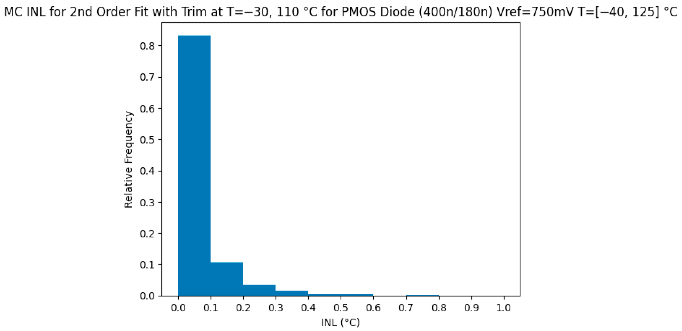
4. Linearity and Yield Evaluation of the Proposed Design

The Diode PMOS with Vref = 0.75 V, W = 400 nm, L = 180 nm sensing unit design will be evaluated to understand how process variations and trim temperatures affect the results. The process variations will cause small changes in the temperature–current relationships, so the IDAC range will need to be larger than the range of the ideal current data. Therefore, denormalized data will be used for curve fitting. A test bench like Figure 3 was used for simulating the new sensing units. This simulation data is used for fitting.
Three trim temperatures will be used for fitting the fitting function. When three trim temperatures are used, the 2nd order polynomial will intersect these three points because it has three degrees of freedom. The temperature step was increased to 0.1 °C to reduce the amount of data being processed from the 400 MC simulations. The standard process variations and mismatch were introduced from the TSMC 180 nm process. The current values from two trim temperatures and 25 °C are used to fit the second order polynomial. The second order fit is used to predict the temperature. Trim at 25 °C is room temperature so oven insertion is not required. The oven trim temperatures were stepped in 5 °C increments.
The best results occur when a low trim temperature and a high trim temperature are used as seen in Table 5. The trim temperatures are notated on the top and left sides. Green values indicate a high yield, while red values indicate a low yield. Yellow values indicate a moderate yield.
The sensing unit renders good results when process variations and trim temperatures are introduced. A yield of 91.25% is achieved with trim temperatures of −30 and 110 °C. A distribution of the INL is shown in Figure 4.
The distribution of the INL shown in the plot is promising. If the INL specification were relaxed to 0.2 °C, the yield would increase to about 94%. Further increase in the INL specification would result in even better yields. This plot confirms that the sensing unit would be a good fit for the architecture. The results for this sensing unit are compared to other works in thermal management in Table 6. Most existing works in this area do not report sensing unit area; however, the area of the sensing unit is exceptionally small compared to existing work that does report the area without sacrificing temperature accuracy or range. This sharp decrease in area would allow for this sensing unit to be placed among dense circuitry. In summary, this work targets minimizing sensing unit area and improving accuracy in a wide temperature sensing range.

5. Conclusions

In this paper, sensing units for a thermal management temperature sensing architecture are analyzed by modeling their temperature–current relationships using fitting functions. Sensing units are selected based on sensing unit area, temperature accuracy, power consumption, and number of parameters in the fitting function. A PMOS W = 400 nm, L = 180 nm, Vref = 750 mV sensing unit is selected for the −40 °C to 125 °C temperature range. This sensing unit has an area of 0.072 µ m 2 excluding area for switches. The temperature accuracy is 0.02 °C when ideal sub-circuit components are used. This design uses three trim temperatures, one room temperature trim, and two oven trims.
The area of this sensing unit is very small compared to existing sensing units, making it able to fit among dense, high-activity circuits. The accuracy is better than many existing temperature sensing units, but is not the standout feature of this design. The temperature range and number of trim temperatures are typical for sensors in thermal management. While these specifications are important, the most beneficial parts of this work might be the characterization and design process. The specific results, like the sensing unit selected, may not translate to other processes like other temperature sensors usually would, because the specifics of the temperature–current relationship may look different in any given process. However, the architectural characterization, and the sensing unit selection process might be the most valuable components of this research. A test bench like Figure 3 could be used to retrieve the temperature current relationship of a sensing unit in any process. The data could be fitted using python in any process. Then trim temperatures could be swept in any process to be optimized based on process and mismatch variations.
There is future work that can be performed with fitting functions. Multiple fitting functions for one sensing unit could be used, and the average or median could be taken. The PMOS W = 400 nm, L = 180 nm, Vref = 750 mV sensing unit has good fitting results using the exponential and power law original data functions, which could be used for this idea. There is also work that can be performed in different processes for this design. The curves of the devices are specific to a given process, so using different processes would likely render different results.

Author Contributions

Conceptualization, S.H. and D.C.; methodology, S.H.; software, S.H.; investigation, S.H.; resources, D.C.; data curation, S.H.; writing—original draft preparation, S.H.; writing—review and editing, S.H. and D.C.; visualization, S.H.; supervision, D.C.; project administration, D.C.; funding acquisition, D.C. All authors have read and agreed to the published version of the manuscript.

Funding

This work was supported in part by the Jerry Junkins Chair Endowment and Iowa State University.

Data Availability Statement

Data was used from simulations in the TSMC 180 nm process.

Conflicts of Interest

The authors declare no conflicts of interest.

References

  1. Fang, Y.; Liu, T.; Sun, D. Research on Novel Thermal Management Technology in the Field of Integrated Circuits. In Proceedings of the 2024 25th International Conference on Electronic Packaging Technology (ICEPT), Tianjin, China, 7–9 August 2024; pp. 1–6. [Google Scholar] [CrossRef]
  2. Singh, P.; Zhuo, C.; Karl, E.; Blaauw, D.; Sylvester, D. Sensor-Driven Reliability and Wearout Management. IEEE Des. Test Comput. 2009, 26, 40–49. [Google Scholar] [CrossRef]
  3. Duarte, D.E.; Taylor, G.; Wong, K.L.; Mughal, U.; Geannopoulos, G. Advanced thermal sensing circuit and test techniques used in a high performance 65 nm processor. In Proceedings of the 2007 International Symposium on Low Power Electronics and Design (ISLPED ′07), Portland, OR, USA, 27–29 August 2007; pp. 304–309. [Google Scholar] [CrossRef]
  4. Zhao, C.; Wang, Y.-T.; Genzer, D.; Chen, D.; Geiger, R. A CMOS on-chip temperature sensor with −0.21 °C 0.17 °C inaccuracy from −20 °C to 100 °C. In Proceedings of the 2013 IEEE International Symposium on Circuits and Systems (ISCAS), Beijing, China, 19–23 May 2013; pp. 2621–2625. [Google Scholar] [CrossRef]
  5. Aprile, A.; Folz, M.; Gardino, D.; Malcovati, P.; Bonizzoni, E. An Area-Efficient Smart Temperature Sensor Based on a Fully Current Processing Error-Feedback Noise-Shaping SAR ADC in 180-nm CMOS. IEEE J. Solid-State Circuits 2023, 59, 716–727. [Google Scholar] [CrossRef]
  6. Tang, J.; Tang, X. A 12.6-pJ/Conversion Temperature Sensor With 0.98-mV/K Temperature-Voltage Sensitivity. IEEE Trans. Circuits Syst. II Express Briefs 2025, 72, 449–453. [Google Scholar] [CrossRef]
  7. Aprile, A.; Bonizzoni, E.; Malcovati, P. Temperature-to-digital converters’ evolution trends and techniques across the last two decades: A review. Micromachines 2022, 13, 2025. [Google Scholar] [CrossRef] [PubMed]
  8. Yang, R.; Gadogbe, B.; Geiger, R.L.; Chen, D. A Compact and Accurate MOS-Based Temperature Sensor for Thermal Management. In Proceedings of the 2023 IEEE 66th International Midwest Symposium on Circuits and Systems (MWSCAS), Tempe, AZ, USA, 6–9 August 2023; pp. 594–598. [Google Scholar] [CrossRef]
  9. Lu, C.-Y.; Ravikumar, S.; Sali, A.D.; Eberlein, M.; Lee, H.-J. An 8b subthreshold hybrid thermal sensor with ±1.07 °C inaccuracy and single-element remote-sensing technique in 22 nm FinFET. In Proceedings of the 2018 IEEE International Solid-State Circuits Conference—(ISSCC), San Francisco, CA, USA, 11–15 February 2018; pp. 318–320. [Google Scholar] [CrossRef]
  10. Luria, K.; Shor, J. Miniaturized CMOS thermal sensor array for temperature gradient measurement in microprocessors. In Proceedings of the 2010 IEEE International Symposium on Circuits and Systems, Paris, France, 30 May–2 June 2010; pp. 1855–1858. [Google Scholar] [CrossRef]
  11. Li, X.; Li, Z.; Zhou, W.; Duan, Z. Accurate On-Chip Temperature Sensing for Multicore Processors Using Embedded Thermal Sensors. IEEE Trans. Very Large Scale Integr. (vlsi) Syst. 2020, 28, 2328–2341. [Google Scholar] [CrossRef]
  12. Sharifi, S.; Rosing, T.Š. Accurate Direct and Indirect On-Chip Temperature Sensing for Efficient Dynamic Thermal Management. IEEE Trans. Comput. Des. Integr. Circuits Syst. 2010, 29, 1586–1599. [Google Scholar] [CrossRef]
  13. Skadron, K.; Stan, M.R.; Huang, W.; Velusamy, S.; Sankaranarayanan, K.; Tarjan, D. Temperature-aware microarchitecture. In Proceedings of the 30th Annual International Symposium on Computer Architecture, San Diego, CA, USA, 9–11 June 2003; pp. 2–13. [Google Scholar] [CrossRef]
  14. Jiang, J.; Shu, W.; Chang, J.; Liu, J. A novel subthreshold voltage reference featuring 17 ppm/°C TC within −40 °C to 125 °C and 75 dB PSRR. In Proceedings of the 2015 IEEE International Symposium on Circuits and Systems (ISCAS), Lisbon, Portugal, 24–27 May 2015; pp. 501–504. [Google Scholar] [CrossRef]
  15. Mittal, R.; Kawoosa, M.; Parekhji, R.A. Systematic approach for trim test time optimization: Case study on a multi-core RF SOC. In Proceedings of the 2014 International Test Conference, Seattle, WA, USA, 23 October 2014; pp. 1–9. [Google Scholar] [CrossRef]
Figure 1. Traditional temperature sensor block diagram.
Metrology 05 00046 g001
Figure 2. Proposed architecture block diagram.
Metrology 05 00046 g002
Figure 3. Test bench for data collection.
Metrology 05 00046 g003
Figure 4. INL distribution for Vref = 750 mV with trim at T = −30, 110 °C.
Metrology 05 00046 g004
Table 1. Fitting functions for modeling temperature–current relationships.
Approximating FunctionEquation
1st Order T = a 1 I + a 0
2nd Order T = a 2 I 2 + a 1 I + a 0
3rd Order T = a 3 I 3 + a 2 I 2 + a 1 I + a 0
4th Order T = a 4 I 4 + a 3 I 3 + a 2 I 2 + a 1 I + a 0
Logarithmic T = a   l n ( I + 1 ) + b
Exponential T = a e b I + c
Power Law T = a I b + c
Power Law Original Data T = a I b + c
3rd Order Fit using CurveFit T = a 3 I 3 + a 2 I 2 + a 1 I + a 0
3 rd   Order   without   x 2 T = a 3 I 3 + a 1 I + a 0
3 rd   Order   without   x 1 T = a 3 I 3 + a 2 I 2 + a 0
3 rd   Order   without   x 0 T = a 3 I 3 + a 2 I 2 + a 1 I
Triode Function I = a T K b ( T K + c )
Saturation Function I = a T K b ( T K + c ) 2
Diode I = a b T K 273.15 e 8695.65 T K
Table 2. Sensing units for initial simulations.
DeviceSize
Diode NMOS(2 µm/180 nm)
Diode NMOS(5 µm/1 µm)
Diode PMOS(2 µm/180 nm)
Diode PMOS(5 µm/1 µm)
Diode–ndio_m(10 µm/10 µm)
Table 3. Sensing units for secondary simulations.
DeviceVrefDimensions
Diode NMOS600 mVW = 2 µm, 1.6 µm, 1.2 µm, 800 nm, 400 nm
L = 180 nm
Diode NMOS550 mV and 750 mVW = 5 µm, 2.5 µm
L = 1 µm, 500 nm
Diode PMOS700 mV, 750 mV,
and 800 mV
W = 2 µm, 1.6 µm, 1.2 µm, 800 nm, 400 nm
L = 180 nm
Diode PMOS650 mV and 700 mVW = 5 µm, 2.5 µm
L = 1 µm, 500 nm
Table 4. Final sensing unit options from simulations.
Sensing UnitFunctionINL (°C)Current Values (µA)
NMOS W = 800 nm, L = 180 nm, Vref = 600 mV 3 rd   Order   without   x 2 0.137.0–18.0
NMOS W = 5 µm, L = 1 µm, Vref = 550 mV3rd Order0.114.2–12.5
PMOS W = 400 nm, L = 180 nm, Vref = 750 mV2nd Order0.024.8–9.6
PMOS W = 2.5 µm, L = 1 µm, Vref = 650 mV3rd Order0.062.1–5.3
Table 5. Yield vs. two trim temperatures for Vref = 750 mV subset.
90 °C95 °C100 °C105 °C110 °C115 °C120 °C125 °C
−40 °C65%72.25%77%84.75%89.5%87.25%85.75%84.5%
−35 °C67%74.25%79%85.75%90.75%89%87.25%85.75%
−30 °C69.75%75.5%81.25%86.25%91.25%90.5%88.25%86.5%
−25 °C72.25%76%83.25%87%86.5%86.25%86.25%86%
−20 °C73.5%78%82%81.25%80.5%80%79.75%79.25%
−15 °C74.5%76%75.75%75.25%74.75%74.75%74.5%74.5%
−10 °C71.25%72.5%72.25%72%72%72%72%72%
Table 6. Results table comparing this work to existing work in thermal management.
SourceProcess Sensing   Unit   Area   ( µ m 2 )INL (°C)Temperature Range
[4]0.18 µm-0.21[−20 °C 100 °C]
[5]0.18 µm-1.96[−50 °C 110 °C]
[6]28 nm-0.15[0 °C 100 °C]
[8]0.18 µm320.6[−20 °C 120 °C]
[9]22 nm2101.07[−30 °C 120 °C]
This Work0.18 µm0.072 *0.02 **[−40 °C 125 °C]
* Does not include area for switches, ** Uses ideal sub-circuit components.
Disclaimer/Publisher’s Note: The statements, opinions and data contained in all publications are solely those of the individual author(s) and contributor(s) and not of MDPI and/or the editor(s). MDPI and/or the editor(s) disclaim responsibility for any injury to people or property resulting from any ideas, methods, instructions or products referred to in the content.

