
Ion Implantation Doping in Silicon Carbide and Gallium Nitride Electronic Devices


Abstract
:1. Introduction
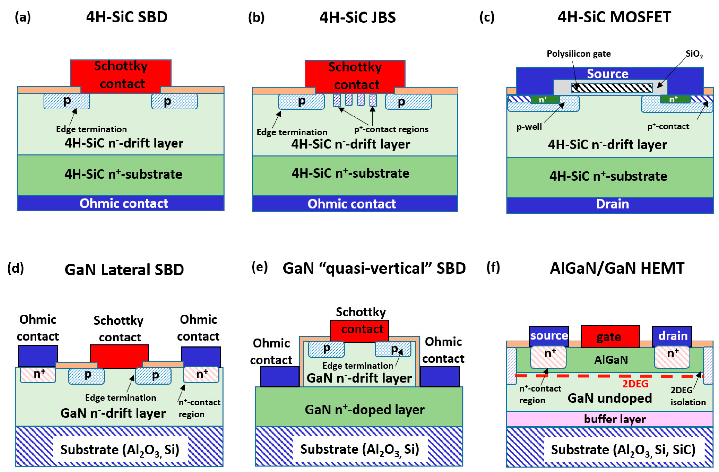
2. Dopant Species in SiC and GaN Power Devices Technology
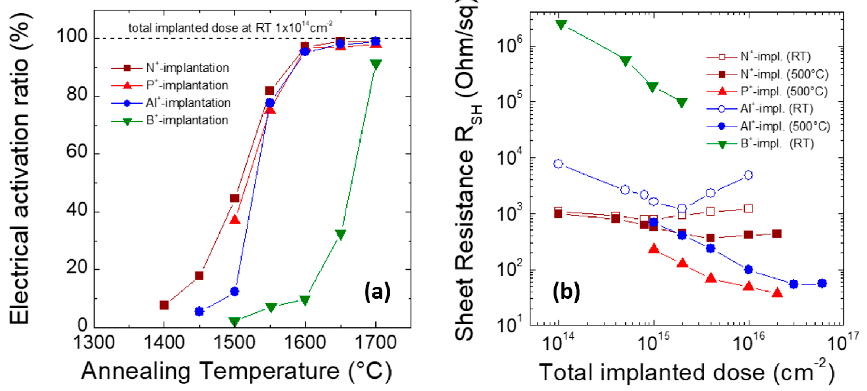
3. Ion Implantation Doping of SiC
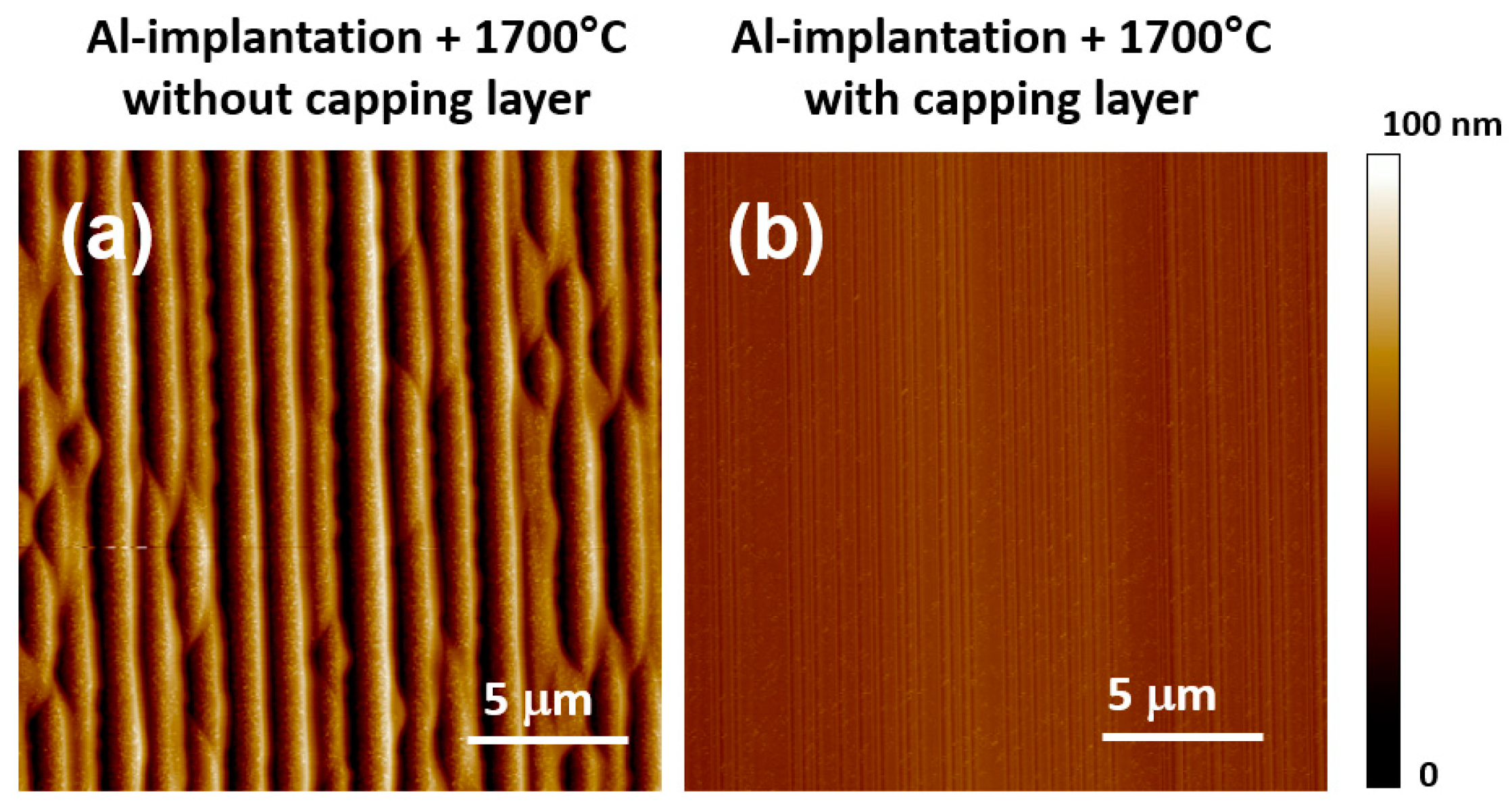
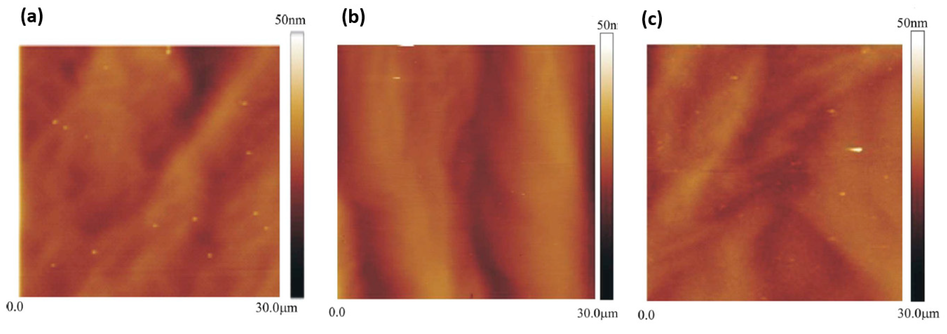
4. Surface Roughness of SiC Layers after Ion Implantation Doping
5. Impact of Ion Implantation Doping on SiC Devices Parameters
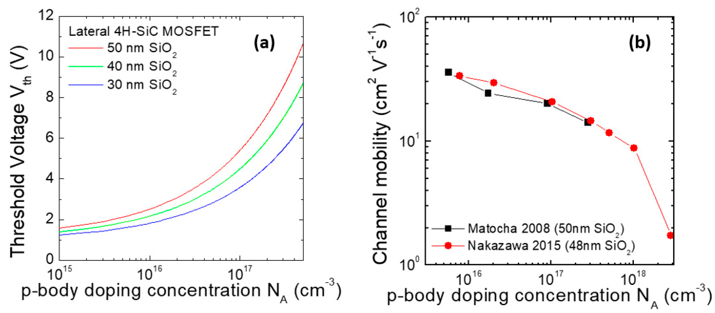
5.1. Doping Effects on 4H-SiC MOSFETs: Threshold Voltage, Channel Mobility and “Counter Doping”
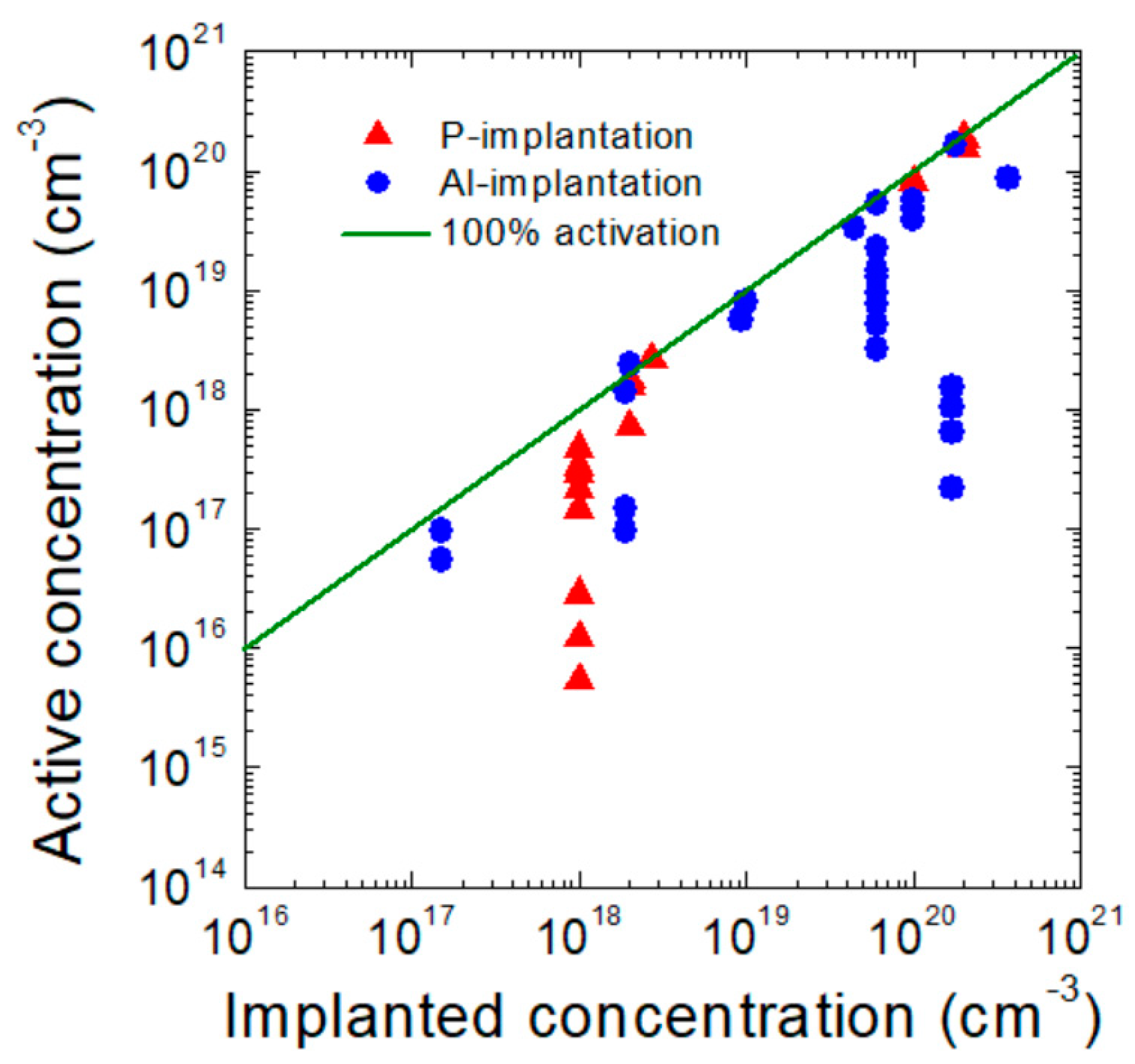
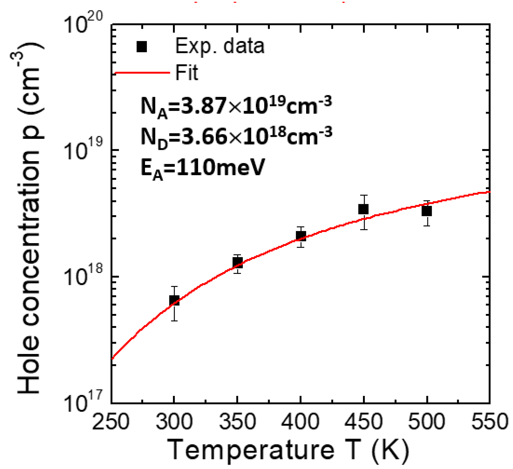
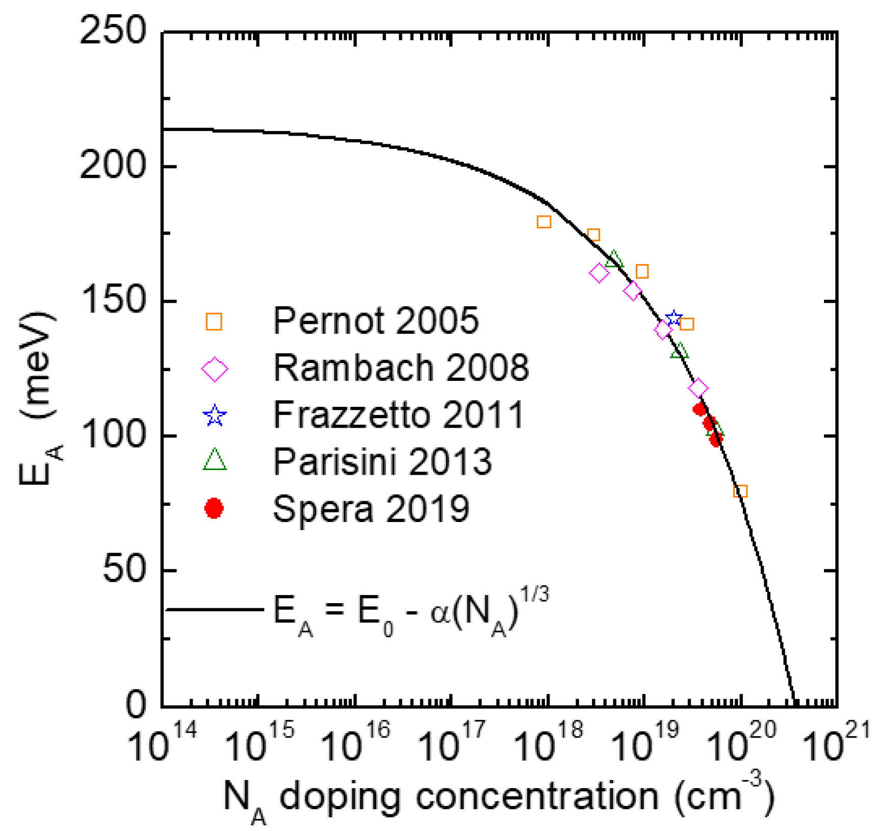
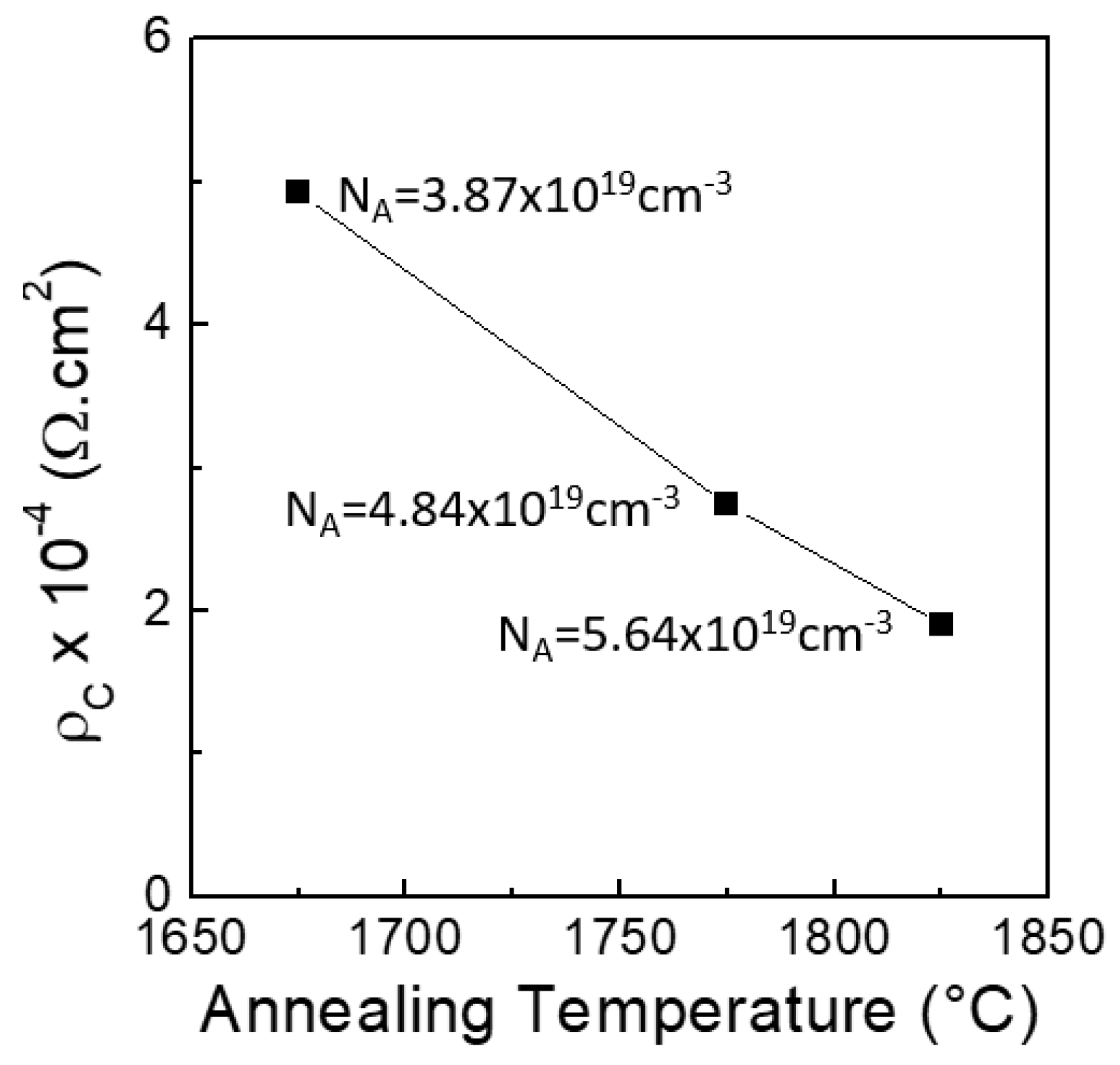
5.2. Heavily Doped N-Type and P-Type Regions for Ohmic Contacts in SiC Devices
6. Ion Implantation Doping of GaN
7. Encapsulation of GaN during Activation Annealing
8. Ion Implantation in GaN HEMT Technology
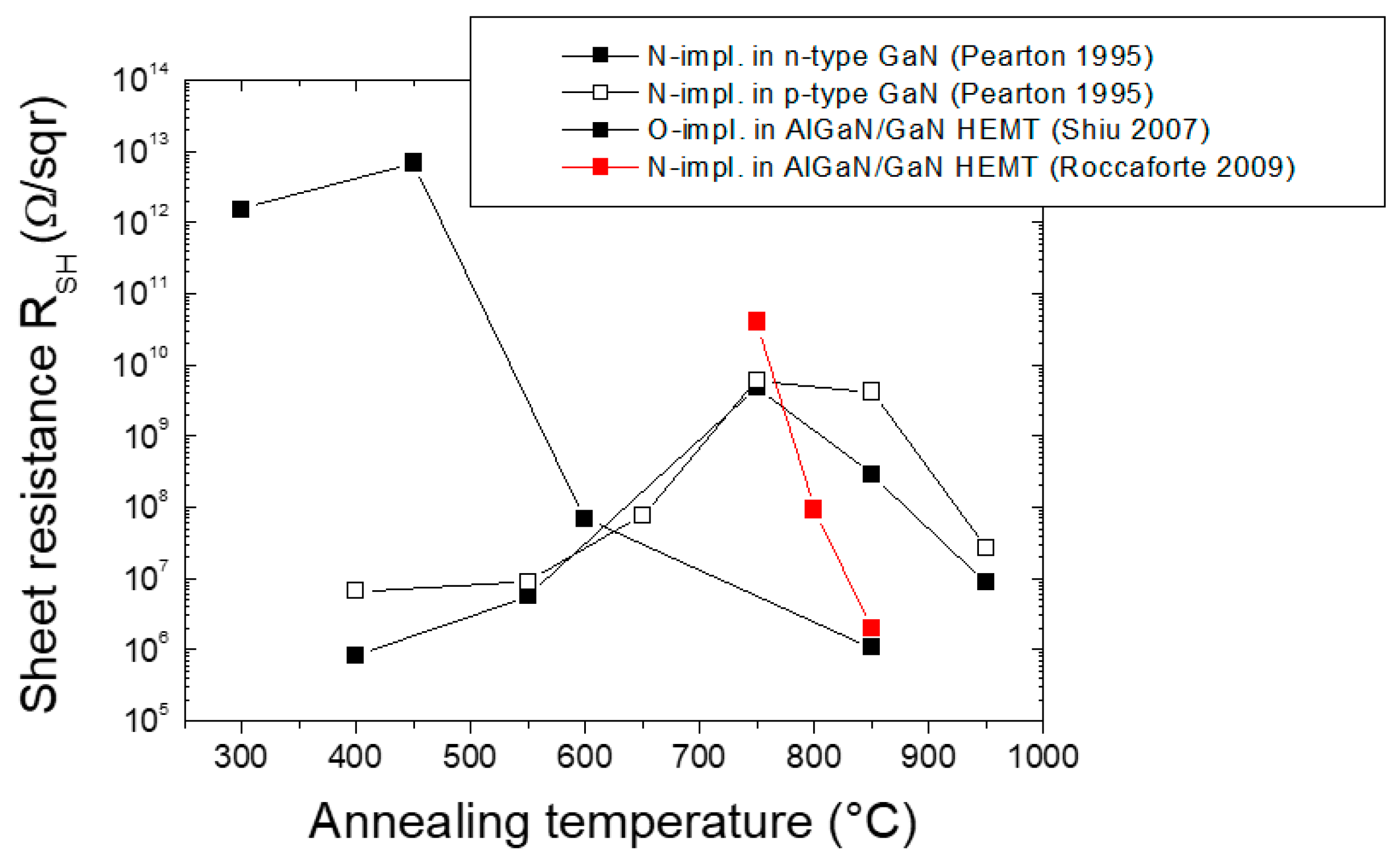
8.1. Two-Dimensional Electron Gas (2DEG) Insulation by Ion Implantation
8.2. N-Type Si-Implantation Doping of GaN for Ohmic Contacts
9. Conclusions
Author Contributions
Funding
Institutional Review Board Statement
Informed Consent Statement
Data Availability Statement
Acknowledgments
Conflicts of Interest
References
- Ren, F.; Zolper, J.C. Wide Band Gap Electronic Devices; World Scientific: Singapore, 2003. [Google Scholar] [CrossRef]
- Kimoto, T.; Cooper, J.A. Fundamentals of Silicon Carbide Technology: Growth, Characterization, Devices and Applications, 1st ed.; John Wiley & Sons: Singapore, 2014. [Google Scholar] [CrossRef]
- Meneghini, M.; Meneghesso, G.; Zanoni, E. Power GaN Devices: Materials, Application and Reliability; Springer International Publishing: Cham, Switzerland, 2017. [Google Scholar] [CrossRef]
- Roccaforte, F.; Leszcyński, M. Nitride Semiconductor Technology: Power Electronics and Optoelectronic Devices, 1st ed.; Wiley-VCH Verlag GmbH & Co. KGaA: Weinheim, Germany, 2020. [Google Scholar] [CrossRef]
- Roccaforte, F.; Fiorenza, P.; Greco, G.; Lo Nigro, R.; Giannazzo, F.; Patti, A.; Saggio, M. Challenges for energy efficient wide band gap semiconductor power devices. Phys. Stat. Sol. A 2014, 211, 2063–2071. [Google Scholar] [CrossRef]
- Kimoto, T. Material science and device physics in SiC technology for high-voltage power devices. Jpn. J. Appl. Phys. 2015, 54, 040103. [Google Scholar] [CrossRef]
- She, X.; Huang, A.Q.; Lucía, Ó.; Ozpineci, B. Review of Silicon Carbide Power Devices and Their Applications. IEEE Trans. Ind. Electron. 2017, 64, 8193–8205. [Google Scholar] [CrossRef]
- Roccaforte, F.; Fiorenza, P.; Greco, G.; Lo Nigro, R.; Giannazzo, F.; Iucolano, F.; Saggio, M. Emerging trends in wide band gap semiconductors (SiC and GaN) technology for power devices. Microelectron. Eng. 2018, 187–188, 66–77. [Google Scholar] [CrossRef]
- Roccaforte, F.; Fiorenza, P.; Lo Nigro, R.; Giannazzo, F.; Greco, G. Physics and technology of gallium nitride materials for power electronics. Riv. Nuovo Cim. 2018, 41, 625–681. [Google Scholar] [CrossRef]
- Amano, H.; Baines, Y.; Beam, E.; Borga, M.; Bouchet, T.; Chalker, P.R.; Charles, M.; Chen, K.J.; Chowdhury, N.; Chu, R.; et al. The 2018 GaN power electronics roadmap. J. Phys. D Appl. Phys. 2018, 51, 163001. [Google Scholar] [CrossRef]
- He, J.; Cheng, W.-C.; Wang, Q.; Cheng, K.; Yu, H.; Chai, Y. Recent Advances in GaN-Based Power HEMT Devices. Adv. Electron. Mater. 2021, 7, 2001045. [Google Scholar] [CrossRef]
- Harris, G.L. Diffusion of Impurities and Ion Implantation. In Properties of Silicon Carbide; Harris, G.L., Ed.; INSPEC, the Institution of Electrical Engineers: London, UK, 1995; pp. 151–157. [Google Scholar]
- Heera, V.; Skorupa, W. Ion implantation and annealing effects in silicon carbide. Mater. Res. Soc. Symp. Proc. 1997, 438, 241–252. [Google Scholar] [CrossRef]
- Svensson, B.G.; Hallén, A.; Linnarsson, M.K.; Kuznetsov, A.Y.; Janson, M.S.; Formanek, B.; Österman, J.; Persson, P.; Hultman, L.; Storasta, L.; et al. Doping of Silicon Carbide by Ion Implantation. Mater. Sci. Forum 2001, 353-356, 549–554. [Google Scholar] [CrossRef]
- Hallén, A.; Janson, M.; Kuznetsov, A.; Åberg, D.; Linnarsson, M.; Svensson, B.; Persson, P.; Carlsson, F.; Storasta, L.; Bergman, J.; et al. Ion implantation of silicon carbide. Nucl. Instr. Methods Phys. Res. B 2002, 186, 186–194. [Google Scholar] [CrossRef]
- Wong-Leung, J.; Janson, M.S.; Kuznetsov, A.; Svensson, B.G.; Linnarsson, M.K.; Hallén, A.; Jagadish, C.; Cockayne, D.J.H. Ion implantation in 4H-SiC. Nucl. Instr. Methods Phys. Res. B 2008, 266, 1367–1372. [Google Scholar] [CrossRef]
- Kimoto, T.; Kawahara, K.; Niwa, H.; Kaji, N.; Suda, J. Ion Implantation Technology in SiC for Power Device Applications. In Proceedings of the 2014 International Workshop on Junction Technology (IWJT), Shanghai, China, 18–20 May 2014; pp. 1–6. [Google Scholar] [CrossRef]
- Lazar, M.; Carole, D.; Raynaud, C.; Ferro, G.; Sejil, S.; Laariedh, F.; Brylinski, C.; Planson, D.; Morel, H. Classic and alternative methods of p-type doping 4H-SiC for integrated lateral devices. In Proceedings of the IEEE 2015 International Semiconductor Conference (CAS), Sinaia, Romania, 12–14 October 2015; pp. 145–148. [CrossRef] [Green Version]
- Hallén, A.; Linnarson, M.K. Ion implantation technology for silicon carbide. Surf. Coat. Technol. 2016, 306, 190–193. [Google Scholar] [CrossRef]
- Nipoti, R.; Ayedh, H.M.; Svensson, B.G. Defects related to electrical doping of 4H-SiC by ion implantation. Mater. Sci. Semicond. Proc. 2018, 78, 13–21. [Google Scholar] [CrossRef]
- Godignon, P.; Torregrosa, F.; Zekentes, K. Silicon Carbide Doping by Ion Implantation. Mater. Res. Found. 2020, 69, 107–174. [Google Scholar] [CrossRef]
- Roccaforte, F.; Fiorenza, P.; Vivona, M.; Greco, G.; Giannazzo, F. Selective Doping in Silicon Carbide Power Devices. Materials 2021, 14, 3923. [Google Scholar] [CrossRef]
- Zolper, J.C.; Hagerott Crawford, M.; Pearton, S.J.; Abernathy, C.R.; Vartuli, C.B.; Yuan, C.; Stall, R.A. Ion implantation and rapid thermal processing of Ill-V nitrides. J. Electr. Mater. 1996, 25, 839–844. [Google Scholar] [CrossRef]
- Tan, H.H.; Williams, J.S.; Zou, J.; Cockayne, J.H.; Pearton, S.J.; Stall, R.A. Damage to epitaxial GaN layers by silicon implantation. Appl. Phys. Lett. 1996, 69, 2364–2366. [Google Scholar] [CrossRef] [Green Version]
- Pearton, S.J.; Zolper, J.C.; Shul, R.J.; Ren, F. GaN: Processing, defects, and devices. J. Appl. Phys. 1999, 86, 1–78. [Google Scholar] [CrossRef]
- Pearton, S.J.; Ren, F.; Zhang, A.P.; Lee, K.P. Fabrication and performance of GaN electronic devices. Mater. Sci. Eng. R 2000, 30, 55–212. [Google Scholar] [CrossRef]
- Kucheyev, S.O.; Williams, J.S.; Pearton, S.J. Ion implantation into GaN. Mater. Sci. Eng. R 2001, 33, 51–108. [Google Scholar] [CrossRef]
- Ronning, C.; Carlson, E.P.; Davis, R.F. Ion implantation into gallium nitride. Phys. Rep. 2011, 351, 349–385. [Google Scholar] [CrossRef]
- Lorenz, K.; Wendler, E. Implantation Damage Formation in GaN and ZnO. In Ion Implantation; Goorsky, M., Ed.; InTech: Rijeka, Croa, 2012; pp. 237–264. [Google Scholar] [CrossRef] [Green Version]
- Feigelson, B.N.; Anderson, T.J.; Abraham, M.; Freitas, J.A.; Hite, J.K.; Eddy, C.R.; Kub, F.J. Multicycle rapid thermal annealing technique and its application for the electrical activation of Mg implanted in GaN. J. Cryst. Growth 2012, 350, 21–26. [Google Scholar] [CrossRef]
- Narita, T.; Kachi, T.; Kataoka, K.; Uesugi, T. P-type doping of GaN(000-1) by magnesium ion implantation. Appl. Phys. Express 2017, 10, 016501. [Google Scholar] [CrossRef]
- Breckenridge, M.H.; Tweedie, J.; Reddy, P.; Guan, Y.; Bagheri, P.; Szymanski, D.; Mita, S.; Sierakowski, K.; Bockowski, M.; Collazo, M.; et al. High Mg activation in implanted GaN by high temperature and ultra high pressure annealing. Appl. Phys. Lett. 2021, 118, 022101. [Google Scholar] [CrossRef]
- Troffer, T.; Schadt, M.; Frank, T.; Itoh, H.; Pensl, G.; Heindl, J.; Strunk, H.P.; Maier, M. Doping of SiC by Implantatin of Boron and Aluminum. Phys. Stat. Sol. A 1997, 162, 277–298. [Google Scholar] [CrossRef]
- Darmody, C.; Goldsman, N. Incomplete ionization in aluminum-doped4H-silicon carbide. J. Appl. Phys. 2019, 126, 145701. [Google Scholar] [CrossRef]
- Gö̈tz, W.W.; Johnson, N.M.; Chen, C.; Liu, H.; Kuo, C.; Imler, W. Activation energies of Si donors in GaN. Appl. Phys. Lett. 1996, 68, 3144–3146. [Google Scholar] [CrossRef]
- Brochen, S.; Brault, J.; Chenot, S.; Dussaigne, A.; Leroux, M.; Damilano, B. Dependence of the Mg-related acceptor ionization energy with the acceptor concentration in p-type GaN layers grown by molecular beam epitaxy. Appl. Phys. Lett. 2013, 103, 032102. [Google Scholar] [CrossRef]
- Chao, L.C.; Steckl, A.J. Room-temperature visible and infrared photoluminescence from Pr-implanted GaN films by focused-ion-beam direct write. Appl. Phys. Lett. 1999, 74, 2364–2366. [Google Scholar] [CrossRef]
- Alves, E.; Monteiro, T.; Soares, J.; Santos, L.; da Silva, M.F.; Soares, J.C.; Lojkowski, W.; Kolesnikov, D.; Vianden, R.; Correia, J.G. High temperature annealing of Er implanted GaN. Mater. Sci. Eng. B 2001, 81, 132–135. [Google Scholar] [CrossRef]
- Pasold, G.; Albrecht, F.; Grillenberger, J.; Grossner, U.; Hülsen, C.; Witthuhn, W.; Sielemann, R. Erbium-related band gap states in 4H– and 6H–silicon carbide. J. Appl. Phys. 2003, 93, 2289–2291. [Google Scholar] [CrossRef]
- Pensl, G.; Ciobanu, F.; Frank, T.; Krieger, M.; Reshanov, S.; Schmid, F.; Weidner, M. SiC Material Properties. In SiC Materials and Devices Vol. I; Shur, M., Rumyanstev, S., Levinshtein, M., Eds.; World Scientific Publishing Co. Pte. Ltd.: Singapore, 2006; pp. 1–41. [Google Scholar] [CrossRef]
- Pearson, G.L.; Bardeen, J. Electrical properties of pure silicon and silicon alloys containing boron and phosphorous. Phys. Rev. 1949, 75, 865–883. [Google Scholar] [CrossRef]
- Efros, A.L.; Lien, N.V.; Shklovskii, B.I. Impurity band structure in lightly doped semiconductors. J. Phys. C Solid State Phys. 1979, 12, 1869–1881. [Google Scholar] [CrossRef]
- Rimini, E. Ion Implantation: Basics to Device Fabrication; Springer: Boston, MA, USA, 1995. [Google Scholar] [CrossRef]
- Kroko, L.J.; Milnes, A.G. Diffusion of nitrogen into silicon carbide single crystals doped with aluminum. Solid-State Electron. 1966, 9, 1125–1130. [Google Scholar] [CrossRef]
- Mokhov, E.N.; Vodakov, Y.A.; Lomakina, G.A. Diffusion of Aluminum in Silicon Carbide. Sov. Phys. Solid State 1969, 11, 415–416. [Google Scholar]
- Krause, O.; Ryssel, H.; Pichler, P. Determination of aluminum diffusion parameters in silicon. J. Appl. Phys. 2002, 91, 5645–5649. [Google Scholar] [CrossRef]
- Mokhov, E.N. Doping of SiC Crystals during Sublimation Growth and Diffusion. In Cystal Growth; Glebovsky, V., Ed.; Intech Open: London, UK, 2019; pp. 1–25. [Google Scholar]
- Jakiela, R.; Barcz, A.; Dumiszewska, E.; Jagoda, A. Si diffusion in epitaxial GaN. Phys. Status Solidi C 2006, 3, 1416–1419. [Google Scholar] [CrossRef]
- Köhler, K.; Gutt, R.; Wiegert, J.; Kirste, L. Diffusion of Mg dopant in metal-organic vapor-phase epitaxy grown GaN and AlxGa1−xN. J. Appl. Phys. 2013, 113, 073514. [Google Scholar] [CrossRef]
- Kelly, M.K.; Ambacher, O.; Dahlheimer, B.; Groos, G.; Dimitrov, R.; Angerer, H.; Stutzmann, M. Optical patterning of GaN films. Appl. Phys. Lett. 1996, 69, 1749–1751. [Google Scholar] [CrossRef]
- Rana, M.A.; Choi, H.W.; Breese, M.B.H.; Osipowicz, T.; Chua, S.J.; Watt, F. A Study of the Decomposition of GaN during Annealing over a Wide Range of Temperatures. MRS Online Proceeding Libr. Arch. 2003, 743, L11.28.1–L11.28.6. [Google Scholar] [CrossRef]
- Choi, H.W.; Cheong, M.G.; Rana, M.A.; Chua, S.J.; Osipowicz, T.; Pan, J.S. Rutherford backscattering analysis of GaN decomposition. J. Vac. Sci. Technol. B 2003, 21, 1080–1083. [Google Scholar] [CrossRef]
- Heera, V.; Stoemenos, J.; Kögler, R.; Skorupa, W. Amorphization and recrystallization of 6H-SiC by ion-beam irradiation. J. Appl. Phys. 1995, 77, 2999–3009. [Google Scholar] [CrossRef]
- Bolse, W.; Conrad, J.; Rödle, T.; Weber, T. Ion-beam-induced amorphization of 6H-SiC. Surf. Coat. Technol. 1995, 74–75, 927–931. [Google Scholar] [CrossRef]
- Kimoto, T.; Inoue, N. Nitrogen Ion Implantation into α-SiC Epitaxial Layers. Phys. Stat. Sol. A 1997, 162, 263–276. [Google Scholar] [CrossRef]
- Negoro, Y.; Miyamoto, N.; Kimoto, T.; Matsunami, H. Remarkable lattice recovery and low sheet resistance of phosphorus implanted 4H-SiC (11–20). Appl. Phys. Lett. 2002, 80, 240–242. [Google Scholar] [CrossRef] [Green Version]
- Kimoto, T.; Takemura, O.; Matsunami, H.; Nakata, T.; Inoue, M. Al+ and B+ implantation into 6H-SiC epilayers and application to pn junction diodes. J. Electr. Mater. 1998, 27, 358–364. [Google Scholar] [CrossRef]
- Negoro, Y.; Kimoto, T.; Matsunami, H.; Schmid, F.; Pensl, G. Electrical activation of high-concentration aluminum implanted in 4H-SiC. J. Appl. Phys. 2004, 96, 4916–4922. [Google Scholar] [CrossRef] [Green Version]
- Capano, M.A.; Santhakumar, R.; Venugopal, R.; Melloch, M.R.; Cooper, J.A. Phosphorus Implantation into 4H-Silicon Carbide. J. Electron. Mater. 2000, 29, 210–214. [Google Scholar] [CrossRef]
- Laube, M.; Schmid, F.; Pensl, G.; Wagner, G.; Linnarsson, M.; Maier, M. Electrical activation of high concentrations of N+ and P+ ions implanted into 4H–SiC. J. Appl. Phys. 2002, 92, 549–554. [Google Scholar] [CrossRef]
- Wendler, E.; Heft, A.; Wesh, W. Ion-beam induced damage and annealing behaviour in SiC. Nucl. Instr. Meth. Phys. B 1998, 141, 105–117. [Google Scholar] [CrossRef]
- Itho, H.; Troffer, T.; Peppermuller, C.; Pensl, G. Effects of C or Si co-implantation on the electrical activation of B atoms implanted in 4H–SiC. Appl. Phys. Lett. 1998, 73, 1427–1429. [Google Scholar] [CrossRef]
- Zhu, L.; Li, Z.; Chow, T.P. N-Type Doping of 4H-SiC with Phosphorus Co-Implanted with C or Si. J. Electron. Mater. 2001, 30, 891–894. [Google Scholar] [CrossRef]
- Pensl, G.; Ciobanu, F.; Frank, T.; Kirmse, D.; Krieger, M.; Reshanov, S.; Schmid, F.; Weidner, W.; Ohshima, T.; Itoh, H.; et al. Defect-engineering in SiC by ion implantation and electron irradiation. Microelectron. Eng. 2006, 83, 146–149. [Google Scholar] [CrossRef]
- Rambach, M.; Frey, L.; Bauer, A.J.; Ryssel, H. Extracting Activation and Compensation Ratio from Aluminum Implanted 4H-SiC by Modeling of Resistivity Measurements. Mater. Sci. Forum 2006, 527–529, 827–830. [Google Scholar] [CrossRef]
- Fujihara, H.; Suda, J.; Kimoto, T. Electrical properties of n- and p-type 4H–SiC formed by ion implantation into high-purity semi-insulating substrates. Jpn. J. Appl. Phys. 2017, 56, 070306. [Google Scholar] [CrossRef]
- Weiße, J.; Hauck, M.; Sledziewski, T.; Tschiesche, M.; Krieger, M.; Bauer, A.J.; Mitlehner, H.; Frey, L.; Erlbacher, T. Analysis of compensation effects in aluminum-implanted 4H–SiC devices. Mater. Sci. Forum 2018, 924, 184–187. [Google Scholar] [CrossRef]
- Weiße, J.; Hauck, M.; Krieger, M.; Bauer, A.J.; Erlbacher, T. Aluminum acceptor activation and charge compensation in implanted p-type 4H-SiC. AIP Adv. 2019, 9, 055308. [Google Scholar] [CrossRef] [Green Version]
- Capano, M.A.; Cooper, J.A.; Melloch, M.R.; Saxler, A.; Mitchel, W.C. Ionization Energies and Electron Mobilities in Phosphorus- and Nitrogen-implanted 4H-Silicon Carbide. J. Appl. Phys. 2000, 87, 8773–8777. [Google Scholar] [CrossRef]
- Saks, N.S.; Agarwal, A.K.; Ryu, S.H.; Palmour, J.W. Low-dose Aluminum and Boron Implants in 4H and 6H Silicon Carbide. J. Appl. Phys. 2001, 90, 2796–2805. [Google Scholar] [CrossRef]
- Senzaki, J.; Fukuda, K.; Arai, K. Influences of Postimplantation Annealing Conditions on Resistance Lowering in High-Phosphorus-Implanted 4H-SiC. J. Appl. Phys. 2003, 94, 2942–2947. [Google Scholar] [CrossRef]
- Sundaresan, S.G.; Rao, M.V.; Tian, Y.-l.; Ridgway, M.C.; Schreifels, J.A.; Kopanski, J.J. Ultrahigh-temperature Microwave Annealing of Al+- and P+-Implanted 4H-SiC. J. Appl. Phys. 2007, 101, 73708. [Google Scholar] [CrossRef] [Green Version]
- Hailei, W.; Guosheng, S.; Ting, Y.; Guoguo, Y.; Lei, W.; Wanshun, Z.; Xingfang, L.; Yiping, Z.; Jialiang, W. Effect of Annealing Process on the Surface Roughness in Multiple Al Implanted 4H-SiC. J. Semicond. 2011, 32, 72002. [Google Scholar] [CrossRef]
- Nipoti, R.; Scaburri, R.; Hallén, A.; Parisini, A. Conventional Thermal Annealing for a more Efficient p-type Doping of Al+ Implanted 4H-SiC. J. Mater. Res. 2013, 28, 17–22. [Google Scholar] [CrossRef]
- Nipoti, R.; Carnera, A.; Alferi, G.; Kranz, L. About the Electrical Activation of 1 × 1020 cm−3 Ion Implanted Al in 4H–SiC at Annealing Temperatures in the Range 1500–1950 °C. Mater. Sci. Forum 2018, 924, 333–338. [Google Scholar] [CrossRef]
- Toifl, A. Modeling and Simulation of Thermal Annealing of Implanted GaN and SiC. Master Thesis, Technical University of Vienna, Vienna, Austra, 2018. Available online: https://www.iue.tuwien.ac.at/uploads/tx_sbdownloader/toifl.pdf (accessed on 16 December 2021).
- Spera, M.; Corso, D.; Di Franco, S.; Greco, G.G.; Severino, A.; Fiorenza, P.; Giannazzo, F.; Roccaforte, F. Effect of high temperature annealing (T > 1650 °C) on the morphological and electrical properties of p-type implanted 4H-SiC layers. Mater. Sci. Semicond. Proc. 2019, 93, 274–279. [Google Scholar] [CrossRef] [Green Version]
- Spera, M.; Greco, G.; Severino, A.; Vivona, M.; Fiorenza, P.; Giannazzo, F.; Roccaforte, F. Active dopant profiling and Ohmic contacts behavior in degenerate n-type implanted silicon carbide. Appl. Phys. Lett. 2020, 117, 013502. [Google Scholar] [CrossRef]
- Nipoti, R.; Parisini, A. Al+ Ion Implanted 4H-SiC: Electrical Activation versus Annealing Time. ECS Trans. 2019, 92, 91–98. [Google Scholar] [CrossRef]
- Šimonka, V.; Toifl, A.; Hössinger, A.; Selberherr, S.; Weinbub, J. Transient model for electrical activation of aluminium and phosphorus-implanted silicon carbide. J. Appl. Phys. 2018, 123, 235701. [Google Scholar] [CrossRef]
- Toifl, A.; Šimonka, V.; Hössinger, A.; Selberherr, S.; Grasser, T. Simulation of the Effects of Postimplantation Annealing on Silicon Carbide DMOSFET Characteristics. IEEE Trans. Electron Dev. 2019, 66, 3060–3065. [Google Scholar] [CrossRef]
- Blanqué, S.; Pérez, R.; Godignon, P.; Mestres, N.; Morvan, E.; Kerlain, A.; Dua, C.; Brylinski, C.; Zielinski, M.; Camassel, J. Room Temperature Implantation and Activation Kinetics of Nitrogen and Phosphorus in 4H-SiC Crystals. Mater. Sci. Forum 2004, 457–460, 893–896. [Google Scholar] [CrossRef]
- Capano, M.A.; Ryu, S.; Cooper, J.A.; Melloch, M.R.; Rottner, K.; Karlsson, S.; Nordell, N.; Powell, A.; Walker, D.E. Surface roughening in ion implanted 4H-silicon carbide. J. Electron. Mater. 1999, 28, 214–218. [Google Scholar] [CrossRef]
- Saddow, S.E.; Williams, J.; Isaacs-Smith, T.; Capano, M.A.; Cooper, J.A.; Mazzola, M.S.; Hsieh, A.J.; Casady, J.B. High temperature implant activation in 4H and 6H-SiC in a silane ambient to reduce step bunching. Mater. Sci. Forum 2000, 338–342, 901–904. [Google Scholar] [CrossRef]
- Rambach, M.; Bauer, A.J.; Ryssel, H. Electrical and topographical characterization of aluminum implanted layers in 4H silicon carbide. Phys. Stat. Sol. B 2008, 245, 1315–1326. [Google Scholar] [CrossRef]
- Weng, M.H.; Roccaforte, F.; Giannazzo, F.; Di Franco, S.; Bongiorno, C.; Zanetti, E.; Ruggiero, A.; Saggio, M.; Raineri, V. Correlation Study of Morphology, Electrical Activation and Contact formation of Ion Implanted 4H-SiC. Solid State Phenom. 2010, 156–158, 493–498. [Google Scholar] [CrossRef]
- Negoro, Y.; Katsumoto, K.; Kimoto, T.; Matsunami, H. Flat Surface after High-Temperature Annealing for Phosphorus-Ion Implanted 4H-SiC(0001) using Graphite Cap. Mater. Sci. Forum 2004, 457–460, 933–936. [Google Scholar] [CrossRef]
- Vassilevski, K.V.; Wright, N.G.; Nikitina, I.P.; Horsfall, A.B.; O’Neill, A.G.; Uren, M.J.; Hilton, K.P.; Masterton, A.G.; Hydes, A.J.; Johnson, C.M. Protection of selectively implanted and patterned silicon carbide surfaces with graphite capping layer during post-implantation annealing. Semicond. Sci. Technol. 2005, 20, 271–278. [Google Scholar] [CrossRef]
- Nipoti, R.; Mancarella, F.; Moscatelli, F.; Rizzoli, R.; Zampolli, S.; Ferri, M. Carbon-Cap for Ohmic Contacts on Ion-Implanted 4H–SiC. Electroch. Solid-State Lett. 2010, 13, H432–H435. [Google Scholar] [CrossRef]
- Frazzetto, A.; Giannazzo, F.; Lo Nigro, R.; Raineri, V.; Roccaforte, F. Structural and transport properties in alloyed Ti/Al Ohmic contacts formed on p-type Al-implanted 4H-SiC annealed at high temperature. J. Phys. D Appl. Phys. 2011, 44, 255302. [Google Scholar] [CrossRef] [Green Version]
- Haney, S.; Agarwal, A. The Effects of Implant Activation Anneal on the Effective Inversion Layer Mobility of 4H-SiC MOSFETs. J. Electron. Mater. 2007, 37, 666–671. [Google Scholar] [CrossRef]
- Naik, H.; Tang, K.; Chow, T.P. Effect of Graphite Cap for Implant Activation on Inversion Channel Mobility in 4H-SiC MOSFETs. Mater. Sci. Forum 2009, 615–617, 773–776. [Google Scholar] [CrossRef]
- Lee, K.L.; Ohshima, T.; Ohi, A.; Itoh, H.; Pensl, G. Anomalous Increase in Effective Channel Mobility on Gamma-Irradiated p-Channel SiC Metal–Oxide–Semiconductor Field-Effect Transistors Containing Step Bunching. Jpn. J. Appl. Phys. 2006, 45, 6830–6836. [Google Scholar] [CrossRef]
- Frazzetto, A.; Giannazzo, F.; Fiorenza, P.; Raineri, V.; Roccaforte, F. Limiting mechanism of inversion channel mobility in Al-implanted lateral 4H-SiC metal-oxide semiconductor field-effect transistors. Appl. Phys. Lett. 2011, 99, 072117. [Google Scholar] [CrossRef]
- Fiorenza, P.; Giannazzo, F.; Frazzetto, A.; Roccaforte, F. Influence of the surface morphology on the channel mobility of lateral implanted 4H-SiC(0001) metal-oxide-semiconductor field-effect transistors. J. Appl. Phys. 2012, 112, 084501. [Google Scholar] [CrossRef] [Green Version]
- Agarwal, A.; Burk, A.; Callanan, R.; Capell, C.; Das, M.; Haney, S.; Hull, B.; Jonas, C.; O’ Loughlin, M.; O’ Neil, M.; et al. Critical Technical Issues in High Voltage SiC Power Devices. Mater. Sci. Forum 2009, 600–603, 895–900. [Google Scholar] [CrossRef]
- Sze, S.M.; Ng, K.K. Physics of Semiconductor Devices; John Wiley & Sons, Inc.: Hoboken, NJ, USA, 2007. [Google Scholar]
- Matocha, K. Challenges in SiC power MOSFET design. Solid-State Electron. 2008, 52, 1631–1635. [Google Scholar] [CrossRef]
- Pérez-Tomás, A.; Brosselard, P.; Godignon, P.; Millán, J.; Mestres, N.; Jennings, M.R.; Covington, J.A.; Mawby, P.A. Field-effect mobility temperature modeling of 4H-SiC metal-oxide-semiconductor transistors. J. Appl. Phys. 2006, 100, 114508. [Google Scholar] [CrossRef]
- Giannazzo, F.; Roccaforte, F.; Raineri, V. Acceptor, compensation, and mobility profiles in multiple Al implanted 4H-SiC. Appl. Phys. Lett. 2007, 91, 202104. [Google Scholar] [CrossRef]
- Nakazawa, S.; Okuda, T.; Suda, J.; Nakamura, T.; Kimoto, T. Interface Properties of 4H-SiC (112¯0) and (11¯00) MOS Structures Annealed in NO. IEEE Trans. Electron Dev. 2015, 62, 309–315. [Google Scholar] [CrossRef]
- Ortiz, G.; Strenger, C.; Uhnevionak, V.; Burenkov, A.; Bauer, A.J.; Pichler, P.; Cristiano, F.; Bedel-Pereira, E.; Mortet, V. Impact of acceptor concentration on electrical properties and density of interface states of 4H-SiC n-metal-oxide-semiconductor field effect transistors studied by Hall effect. Appl. Phys. Lett. 2015, 106, 062104. [Google Scholar] [CrossRef] [Green Version]
- Ueno, K.; Oikawa, T. Counter-doped MOSFETs of 4H-SiC. IEEE Electron Device Lett. 1999, 20, 624–626. [Google Scholar] [CrossRef]
- Moscatelli, F.; Poggi, A.; Solmi, S.; Nipoti, R. Nitrogen Implantation to Improve Electron Channel Mobility in 4H-SiC MOSFET. IEEE Trans. Electron Dev. 2008, 55, 961–967. [Google Scholar] [CrossRef]
- Cabello, M.; Soler, V.; Rius, G.; Montserrat, J.; Rebollo, J.; Godignon, P. Advanced processing for mobility improvement in 4H-SiC MOSFETs: A review. Mater. Sci. Semicond. Proc. 2018, 78, 22–31. [Google Scholar] [CrossRef]
- Swanson, L.K.; Fiorenza, P.; Giannazzo, F.; Frazzetto, A.; Roccaforte, F. Correlating macroscopic and nanoscale electrical modifications of SiO2/4H-SiC interfaces upon post-oxidation-annealing in N2O and POCl3. Appl. Phys. Lett. 2012, 101, 193501. [Google Scholar] [CrossRef]
- Fiorenza, P.; Giannazzo, F.; Vivona, M.; La Magna, A.; Roccaforte, F. SiO2/4H-SiC interface doping during post-deposition-annealing of the oxide in N2O or POCl3. Appl. Phys. Lett. 2013, 103, 153508. [Google Scholar] [CrossRef]
- Modic, A.; Liu, G.; Ahyi, A.C.; Zhou, Y.; Xu, P.; Hamilton, M.C.; Williams, J.R.; Feldman, L.C.; Dhar, S. High channel mobility 4H-SiC MOSFETs by antimony counter-doping. IEEE Electron Device Lett. 2014, 35, 894–896. [Google Scholar] [CrossRef]
- Pernot, J.; Contreras, S.; Camassel, J. Electrical transport properties of aluminium implanted 4H-SiC. J. Appl. Phys. 2005, 98, 023706. [Google Scholar] [CrossRef]
- Parisini, A.; Nipoti, R. Analysis of the hole transport through valence band states in heavy Al doped 4H-SiC by ion implantation. J. Appl. Phys. 2013, 114, 243703. [Google Scholar] [CrossRef]
- Contreras, S.; Konczewicz, L.; Arvinte, R.; Peyre, H.; Chassagne, T.; Zielinski, M.; Juillaguet, S. Electrical transport properties of p-type 4H-SiC. Phys. Stat. Sol. A 2017, 214, 1600679. [Google Scholar] [CrossRef] [Green Version]
- Pensl, G.; Schmid, F.; Ciobanu, F.; Laube, M.; Reshanov, S.A.; Schulze, N.; Semmelroth, K.; Nagasawa, H.; Schöner, A.; Wagner, G. Electrical and optical characterization of SiC. Mater. Sci. Forum 2003, 433–436, 365–370. [Google Scholar] [CrossRef]
- Asada, S.; Okuda, T.; Kimoto, T.; Suda, J. Hall scattering factors in p-type 4H-SiC with various doping concentrations. Appl. Phys. Express 2016, 9, 041301. [Google Scholar] [CrossRef]
- Schorder, D.K. Semiconductor Material and Device Characterization, 3rd ed.; John Wiley & Sons, Inc.: Hoboken, NJ, USA, 2006. [Google Scholar]
- Rambach, M.; Bauer, A.J.; Ryssel, H. High Temperature Implantation of Aluminum in 4H Silicon Carbide. Mater. Sci. Forum 2007, 556–557, 587–590. [Google Scholar] [CrossRef]
- Roccaforte, F.; Frazzetto, A.; Greco, G.; Giannazzo, F.; Fiorenza, P.; Lo Nigro, R.; Saggio, M.; Leszczyński, M.; Prystawko, P.; Raineri, V. Critical issues for interfaces to p-type SiC and GaN in power devices. Appl. Surf. Sci. 2012, 258, 8324–8333. [Google Scholar] [CrossRef]
- Fisher, A.A.; Jennings, M.; Sharma, Y.K.; Sanchez-Fuentes, A.; Walker, D.; Gammon, P.M.; Pérez-Tomás, A.; Thomas, S.M.; Burrows, S.E.; Mawby, P.A. On the Schottky Barrier Height Lowering Effect of Ti3SiC2 in Ohmic Contacts to P-Type 4H-SiC. Intern. J. Fund. Phys. Sci. 2014, 4, 95–100. [Google Scholar] [CrossRef]
- Abi-Tannous, T.; Souedain, M.; Ferro, G.; Lazar, M.; Raynaud, C.; Toury, B.; Beaufort, M.F.; Barbot, J.F.; Dezellus, O.; Planson, D. A Study on the Temperature of Ohmic Contact to p-Type SiC Based on Ti3SiC2 Phase. IEEE Trans. Electron Dev. 2016, 63, 2462. [Google Scholar] [CrossRef] [Green Version]
- Vivona, A.; Greco, G.; Lo Nigro, R.; Bongiorno, C.; Roccaforte, F. Ti/Al/W Ohmic contacts to p-type implanted 4H-SiC. J. Appl. Phys. 2015, 118, 035705. [Google Scholar] [CrossRef]
- Vivona, M.; Greco, G.; Bongiorno, C.; Lo Nigro, R.; Scalese, S.; Roccaforte, F. Electrical and structural properties of surfaces and interfaces in Ti/Al/Ni Ohmic contacts to p-type implanted 4H-SiC. Appl. Surf. Sci. 2017, 420, 331–335. [Google Scholar] [CrossRef]
- Spera, M.; Greco, G.; Corso, D.; Di Franco, S.; Severino, A.; Messina, A.A.; Giannazzo, F.; Roccaforte, F. Ohmic Contacts on p-Type Al-Implanted 4H-SiC Layers after Different Post-Implantation Annealings. Materials 2019, 12, 3468. [Google Scholar] [CrossRef] [Green Version]
- Nipoti, R.; Nath, A.; Qadri, S.B.; Tian, Y.-L.; Albonetti, C.; Carnera, A.; Rao, M.V. High-Dose Phosphorus-Implanted 4H-SiC: Microwave and Conventional Post-Implantation Annealing at Temperatures ≥ 1700C. J. Electron. Mater. 2012, 41, 457–465. [Google Scholar] [CrossRef]
- Schmid, F.; Laube, M.; Pensl, G.; Wagner, G.; Maier, M. Electrical activation of implanted phosphorus ions in [0001]- and [11-20]-oriented 4H-SiC. J. Appl. Phys. 2002, 91, 9182–9186. [Google Scholar] [CrossRef]
- Pankove, J.I.; Hutchby, J.A. Photoluminescence of Zn-implanted GaN. Appl. Phys. Lett. 1974, 24, 281–283. [Google Scholar] [CrossRef]
- Pankove, J.I.; Hutchby, J.A. Photoluminescence of ion-implanted GaN. J. Appl. Phys. 1976, 47, 5387–5390. [Google Scholar] [CrossRef]
- Pearton, S.J.; Vartuli, C.B.; Zolper, J.C.; Yuan, C.; Stall, R.A. Ion implantation doping and isolation of GaN. Appl. Phys. Lett. 1995, 67, 1435–1437. [Google Scholar] [CrossRef]
- Zolper, J.C.; Wilson, R.G.; Pearton, S.J.; Stall, R.A. Ca and O ion implantation doping of GaN. Appl. Phys. Lett. 1996, 68, 1945–1947. [Google Scholar] [CrossRef]
- Irokawa, Y.; Fujishima, O.; Kachi, T.; Pearton, S.J.; Ren, F. Electrical characteristics of GaN implanted with Si+ at elevated temperatures. Appl. Phys. Lett. 2005, 86, 112108. [Google Scholar] [CrossRef]
- Irokawa, Y.; Fujishima, O.; Kachi, T.; Nakano, Y. Electrical activation characteristics of silicon-implanted GaN. J. Appl. Phys. 2005, 97, 083505. [Google Scholar] [CrossRef]
- Wenzel, A.; Liu, C.; Rauschenbach, B. Effect of implantation-parameters on the structural properties of Mg-ion implanted GaN. Mater. Sci. Eng. B 1999, 59, 191–194. [Google Scholar] [CrossRef]
- Kobayashi, H.; Gibson, W.M. Lattice location of Si in ion implanted GaN. Appl. Phys. Lett. 1998, 73, 1406–1408. [Google Scholar] [CrossRef]
- Iucolano, F.; Giannazzo, F.; Roccaforte, F.; Romano, L.; Grimaldi, M.G.; Raineri, V. Quantitative determination of depth carrier profiles in ion-implanted Gallium Nitride. Nucl. Instr. Methods Phys. Res. B 2007, 257, 336–339. [Google Scholar] [CrossRef]
- Iucolano, F.; Giannazzo, F.; Roccaforte, F.; Puglisi, V.; Grimaldi, M.G.; Raineri, V. Effects of thermal annealing in ion-implanted Gallium Nitride. In Proceedings of the 15th IEEE International Conference on Advanced Thermal Processing of Semiconductors (RTP2007), Catania, Italy, 2–5 October 2007; pp. 161–163. [Google Scholar] [CrossRef]
- Lamhamdi, M.; Cayrel, F.; Bazin, A.E.; Collard, E.; Alquier, D. Carrier profiling in Si-implanted gallium nitride by Scanning Capacitance Microscopy. Nucl. Instr. Methods Phys. Res. B 2012, 275, 37–40. [Google Scholar] [CrossRef]
- Liu, K.T.; Su, Y.K.; Chang, S.J.; Horikoshi, Y. Magnesium/nitrogen and beryllium/nitrogen coimplantation into GaN. J. Appl. Phys. 2005, 98, 073702. [Google Scholar] [CrossRef]
- Oikawa, T.; Saijo, Y.; Kato, S.; Mishima, T.; Nakamura, T. Formation of definite GaN p–n junction by Mg-ion implantation to n-GaN epitaxial layers grown on a high-quality free-standing GaN substrate. Nucl. Instr. Methods Phys. Res. B 2015, 365, 168–170. [Google Scholar] [CrossRef]
- Niwa, T.; Fujii, T.; Oka, T. High carrier activation of Mg ion-implanted GaN by conventional rapid thermal annealing. Appl. Phys. Express 2017, 10, 091002. [Google Scholar] [CrossRef]
- Alves, H.; Leiter, F.; Pfisterer, D.; Hofmann, D.M.; Meyer, B.K.; Einfeld, S.; Heinke, H.; Hommel, D. Mg in GaN: The structure of the acceptor and the electrical activity. Phys. Stat. Sol. C 2003, 1770–1782. [Google Scholar] [CrossRef]
- Porowski, S.; Grzegory, I.; Kolesnikov, D.; Lojkowski, W.; Jager, V.; Jager, W.; Bogdanov, V.; Suski, T.; Krukowski, S. Annealing of GaN under high pressure of nitrogen. J. Phys. Condens. Matter 2002, 14, 11097–11110. [Google Scholar] [CrossRef]
- Anderson, T.J.; Feigelson, B.N.; Kub, F.J.; Tadjer, M.J.; Hobart, K.D.; Mastro, M.A.; Hite, J.K.; Eddy, C.R. Activation of Mg implanted in GaN by multicycle rapid thermal annealing. Electron. Lett. 2014, 50, 197–198. [Google Scholar] [CrossRef]
- Anderson, T.J.; Gallagher, J.C.; Luna, L.E.; Koehler, A.D.; Jacobs, A.G.; Xie, J.; Beam, E.; Hobart, K.D.; Feigelson, B.N. Effect of high temperature, high pressure annealing on GaN drift layers for vertical power devices. J. Cryst. Growth 2018, 499, 35–39. [Google Scholar] [CrossRef]
- Aluri, G.S.; Gowda, M.; Mahadik, N.A.; Sundaresan, S.G.; Rao, M.V.; Schreifels, J.A.; Freitas, J.A.; Qadri, S.B.; Tian, Y.-L. Microwave annealing of Mg-implanted and in situ Be-doped GaN. J. Appl. Phys. 2010, 108, 083103. [Google Scholar] [CrossRef]
- Meyers, V.; Rocco, E.; Anderson, T.J.; Gallagher, J.C.; Ebrish, M.A.; Jones, K.; Derenge, M.; Shevelev, M.; Sklyar, V.; Hogan, K.; et al. P-type conductivity and damage recovery in implanted GaN annealed by rapid gyrotron microwave annealing. J. Appl. Phys. 2020, 128, 085701. [Google Scholar] [CrossRef]
- Sakurai, H.; Omori, M.; Yamada, S.; Furukawa, Y.; Suzuki, H.; Narita, T.; Kataoka, K.; Horita, M.; Bockowski, M.; Suda, J.; et al. Highly effective activation of Mg-implanted p-type GaN by ultra-high-pressure annealing. Appl. Phys. Lett. 2019, 115, 142104. [Google Scholar] [CrossRef]
- Placidi, M.; Pérez-Tomás, A.; Constant, A.; Rius, G.; Mestres, N.; Millán, J.; Godignon, P. Effects of cap layer on ohmic Ti/Al contacts to Si+-implanted GaN. Appl. Surf. Sci. 2009, 255, 6057–6060. [Google Scholar] [CrossRef]
- Yu, H.; McCarthy, L.; Rajan, S.; Keller, S.; Denbaars, S.; Speck, J.; Mishra, U. Ion implanted AlGaN-GaN HEMTs with nonalloyed ohmic contacts. IEEE Electron Device Lett. 2005, 26, 283–285. [Google Scholar] [CrossRef]
- Pérez-Tomás, A.; Placidi, M.; Baron, N.; Chenot, S.; Cordier, Y.; Moreno, J.C.; Constant, A.; Godignon, P.; Millán, J. GaN transistor characteristics at elevated temperatures. J. Appl. Phys. 2009, 106, 074519. [Google Scholar] [CrossRef]
- Ostermaier, C.; Ahn, S.I.; Potzger, K.; Helm, M.; Kuzmik, J.; Pogany, D.; Strasser, G.; Lee, J.H.; Hahm, S.H.; Lee, J.H. Study of Si Implantation into Mg-doped GaN for MOSFETs. Phys. Stat. Sol. C 2010, 7, 1964–1966. [Google Scholar] [CrossRef]
- Matsunaga, S.; Yoshida, S.; Kawaji, T.; Inada, T. Silicon implantation in epitaxial GaN layers: Encapsulant annealing and electrical properties. J. Appl. Phys. 2004, 95, 2461–2466. [Google Scholar] [CrossRef]
- Hager, C.E.; Jones, K.A.; Derenge, M.A.; Zheleva, T.S. Activation of ion implanted Si in GaN using a dual AlN annealing cap. J. Appl. Phys. 2009, 105, 033713. [Google Scholar] [CrossRef]
- Zolper, J.C.; Rieger, D.J.; Baca, A.G.; Peraton, S.J.; Lee, J.T.; Stall, R.A. Sputtered AlN encapsulant for high- temperature annealing of GaN. Appl. Phys. Lett. 1996, 69, 538–540. [Google Scholar] [CrossRef]
- Khalfaoui, W.; Oheix, T.; El-Zammar, G.; Benoit, R.; Cayrel, F.; Faulques, E.; Massuyeau, F.; Yvon, A.; Collard, E.; Alquier, D. Impact of rapid thermal annealing on Mg-implanted GaN with a SiOx/AlN cap-layer. Phys. Status Solidi A 2017, 214, 1600438. [Google Scholar] [CrossRef]
- Lardeau-Falcy, A.; Coig, M.; Charles, M.; Licitra, C.; Baines, Y.; Eymery, J.; Mazen, F. Capping stability of Mg-implanted GaN layers grown on silicon. Phys. Stat. Sol. A 2017, 214, 1600487. [Google Scholar] [CrossRef]
- Iucolano, F.; Roccaforte, F.; Giannazzo, F.; Raineri, V. Influence of high-temperature GaN annealed surface on the electrical properties of Ni/GaN Schottky contacts. J. Appl. Phys. 2008, 104, 093706. [Google Scholar] [CrossRef]
- Pearton, S.J.; Abernathy, C.R.; Ren, F. Gallium Nitride Processing for Electronics, Sensors and Spintronics; Springer: London, UK, 2006. [Google Scholar] [CrossRef]
- Liu, L.; Zhu, T.G.; Murphy, M.; Pabisz, M.; Pophristic, M.; Peres, B.; Hierl, T. 600V GaN Schottky Barrier Power Devices for High Volume and Low Cost Applications. Mater. Sci. Forum 2009, 600–603, 1251–1256. [Google Scholar] [CrossRef]
- Alquier, D.; Cayrel, F.; Menard, O.; Bazin, A.-E.; Yvon, A.; Collard, E. Recent Progresses in GaN Power Rectifier. Jpn. J. Appl. Phys. 2012, 51, 01AG08-1–01AG08-7. [Google Scholar] [CrossRef]
- Roccaforte, F.; Giannazzo, F.; Iucolano, F.; Eriksson, J.; Weng, H.H.; Raineri, V. Surface and interface issues in wide band gap semiconductor electronics. Appl. Surf. Sci. 2010, 256, 5727–5735. [Google Scholar] [CrossRef]
- Özdemir, A.F.; Türüt, A.; Kőkçe, A. The interface state energy distribution from capacitance–frequency characteristics of gold/n-type Gallium Arsenide Schottky barrier diodes exposed to air. Thin Solid Film. 2003, 425, 210–215. [Google Scholar] [CrossRef]
- Binari, S.C.; Dietrich, H.B.; Kelner, G.; Rowland, L.B.; Doverspike, K.J.; Wickenden, D.K. H, He and N implant isolation of n-type GaN. J. Appl. Phys. 1995, 78, 3008–3011. [Google Scholar] [CrossRef]
- Wilson, R.G.; Vartuli, C.B.; Abernathy, C.R.; Pearton, S.J.; Zavada, J.M. Implantation and redistribution of dopants and isolation species in GaN and related compounds. Solid State Electron. 1995, 38, 1435–1437. [Google Scholar] [CrossRef]
- Zolper, J.C. Ion implantation in group III-nitride semiconductors: A tool for doping and defect studies. J. Cryst. Growth 1997, 178, 157–167. [Google Scholar] [CrossRef]
- Boudart, B.; Guhel, Y.; Pesant, J.C.; Dhamelincourt, P.; Poisson, M.A. Raman characterization of Ar+ ion-implanted GaN. J. Raman Spectrosc. 2002, 33, 283–286. [Google Scholar] [CrossRef]
- Boudart, B.; Guhel, Y.; Pesant, J.C.; Dhamelincourt, P.; Poisson, M.A. Raman characterization of Mg+ ion-implanted GaN. J. Phys. Condens. Matter 2004, 16, s49–s55. [Google Scholar] [CrossRef]
- Oishi, T.; Miura, N.; Suita, M.; Nanjo, T.; Abe, Y.; Ozeki, T.; Ishikawa, H.; Egawa, T.; Jimbo, T. Highly resistive GaN layers formed by ion implantation of Zn along the c-axis. J. Appl. Phys. 2003, 94, 1662–1666. [Google Scholar] [CrossRef]
- Dang, G.; Cao, X.A.; Ren, F.; Pearton, S.J.; Han, J.; Baca, A.G.; Shul, R.J.; Wilson, R.G. Comparison of Implant Isolation Species for GaN Field-Effect Transistor Structures. MRS Online Proc. Libr. 1999, 595, 1168. [Google Scholar] [CrossRef]
- Boudinov, H.; Kucheyev, S.O.; Williams, J.S.; Jagadish, C.; Li, G. Electrical isolation of GaN by MeV ion irradiation. Appl. Phys. Lett. 2001, 78, 943–945. [Google Scholar] [CrossRef]
- Shiu, J.-Y.; Huang, J.-C.; Desmaris, V.; Chang, C.-T.; Lu, C.-Y.; Kumakura, K.; Makimoto, T.; Zirath, H.; Rorsman, N.; Chang, E.Y. Oxygen Ion Implantation Isolation Planar Process for AlGaN/GaN HEMTs. IEEE Electron Device Lett. 2007, 28, 476–478. [Google Scholar] [CrossRef] [Green Version]
- Roccaforte, F.; Iucolano, F.; Giannazzo, F.; Moschetti, G.; Bongiorno, C.; Di Franco, S.; Puglisi, V.; Abbondanza, G.; Raineri, V. Influence of Thermal Annealing on Ohmic Contacts and Device Isolation in AlGaN/GaN Heterostructures. Mater. Sci. Forum 2009, 615-617, 967–970. [Google Scholar] [CrossRef]
- Greco, G.; Iucolano, F.; Roccaforte, F. Ohmic contacts to Gallium Nitride materials. Appl. Surf. Sci. 2016, 383, 324–345. [Google Scholar] [CrossRef]
- Greco, G.; Iucolano, F.; Bongiorno, C.; Giannazzo, F.; Krysko, M.; Leszczynski, M.; Roccaforte, F. Ti/Al ohmic contacts on AlGaN/GaN heterostructures with different defect density. Appl. Surf. Sci. 2014, 314, 546–551. [Google Scholar] [CrossRef]
- Greco, G.; Giannazzo, F.; Iucolano, F.; Lo Nigro, R.; Roccaforte, F. Nanoscale structural and electrical evolution of Ta- and Ti-based contacts on AlGaN/GaN heterostructures upon annealing. J. Appl. Phys. 2013, 114, 083717. [Google Scholar] [CrossRef]
- Spera, M.; Greco, G.; Nigro, R.L.; Bongiorno, C.; Cannas, M.; Giannazzo, F. Metal/semiconductor barrier properties of non-recessed Ti/Al/Ti and Ta/Al/Ta Ohmic contacts on AlGaN/GaN heterostructures. Energies 2019, 12, 2655. [Google Scholar] [CrossRef] [Green Version]
- Sheu, J.K.; Tun, C.J.; Tsai, M.S.; Lee, C.C.; Chi, G.C.; Chang, S.J.; Su, Y.K. N+-GaN formed by Si implantation into p-GaN. J. Appl. Phys. 2002, 91, 1845–1848. [Google Scholar] [CrossRef]
- Pérez-Tomás, A.; Fontserè, A.; Placidi, M.; Jennings, M.R.; Gammon, P.M. Modelling the metal-semiconductor band structure in implanted ohmic contacts to GaN and SiC. Model. Simul. Mater. Sci. Eng. 2013, 21, 035004. [Google Scholar] [CrossRef]
- Lester, L.F.; Brown, J.M.; Ramer, J.C.; Zhang, L.; Hersee, S.D.; Zolper, J.C. Nonalloyed Ti/Al Ohmic contacts to n-type GaN using high-temperature premetallization anneal. Appl. Phys. Lett. 1996, 69, 2737–2739. [Google Scholar] [CrossRef]
- Burm, J.; Chu, K.; Davis, W.A.; Schaff, W.J.; Eastman, L.F.; Eustis, T.J. Ultra-low resistive ohmic contacts on n-GaN using Si implantation. Appl. Phys. Lett. 1997, 70, 464–466. [Google Scholar] [CrossRef]
- Kozubal, M.A.; Karolina, P.; Andrzej, T.; Renata, K.; Iwona, S.; Eliana, K. Ohmic contact formation to GaN by Si+ implantation doping: Retarding layer, implantation fluence, encapsulation, and activation annealing temperature studies. Mater. Sci. Semicond. Proc. 2021, 122, 1–9. [Google Scholar] [CrossRef]
- Nguyen, C.; Shah, P.; Leong, E.; Derenge, M.; Jones, K. Si implant-assisted Ohmic contacts to GaN. Solid. State. Electron. 2010, 54, 1227–1231. [Google Scholar] [CrossRef] [Green Version]
- Qiao, D.; Guan, Z.F.; Carlton, J.; Lau, S.S.; Sullivan, G.J. Low resistance ohmic contacts on AlGaN/GaN structures using implantation and the “advancing” Al/Ti metallization. Appl. Phys. Lett. 1999, 74, 2652–2654. [Google Scholar] [CrossRef]
- Recht, F.; McCarthy, L.; Rajan, S.; Chakraborty, A.; Poblenz, C.; Corrion, A.; Speck, J.S.; Mishra, U.K. Nonalloyed ohmic contacts in AlGaN/GaN HEMTs by ion implantation with reduced activation annealing temperature. IEEE Electron Device Lett. 2006, 27, 205–207. [Google Scholar] [CrossRef] [Green Version]
- Nomoto, K.; Tajima, T.; Mishima, T.; Satoh, M.; Nakamura, T. Remarkable reduction of on-resistance by ion implantation in GaN/AlGaN/GaN HEMTs with low gate leakage current. IEEE Electron Device Lett. 2007, 28, 939–941. [Google Scholar] [CrossRef]


| Material | N-Type Dopant | P-Type Dopant |
|---|---|---|
| SiC | N, P (~60 meV) | Al (~200 meV); B (280–300 meV) |
| GaN | Si (12–62 meV) | Mg (170–245 meV) |
| Implanted Region | Doping Level (cm−3) | Implantation Depth (μm) |
|---|---|---|
| Source/Drain, n+-contacts | 1019–1020 | 0.2–0.3 |
| MOSFET p-body | 1017–1018 | 0.4–0.8 |
| p+-contacts | 1019–1020 | 0.2–0.3 |
| Edge termination | 1016–1017 | 0.4–0.8 |
| 2DEG isolation | N.A. | 0.1–0.2 |
| Ann. Temp. (°C) | Resistivity (Ω cm) | EA (meV) | NA (cm−3) | ND (cm−3) | Al Activation | Compensation ND/NA |
|---|---|---|---|---|---|---|
| 1675 | 0.36 | 110 | 3.87 × 10¹⁹ | 3.66 × 10¹⁸ | 39% | 9.4% |
| 1775 | 0.29 | 105 | 4.84 × 10¹⁹ | 3.49 × 10¹⁸ | 48% | 7.2% |
| 1825 | 0.22 | 99 | 5.64 × 10¹⁹ | 3.48 × 10¹⁸ | 56% | 6.2% |
| Material | Implantation/Activation | Contact Formation | ρc (Ωcm2) | Ref. |
|---|---|---|---|---|
| p-GaN |
|
| 1.0 × 10⁻⁵ Ωcm2 | [145] |
| p-GaN |
|
| 1.5 × 10⁻⁶ Ωcm2 | [174] |
| p-GaN |
|
| 2.0 × 10⁻⁴ Ωcm2 | [175] |
| n-GaN |
|
| 1.0 × 10⁻⁵ Ωcm2 | [176] |
| n-GaN |
|
| 3.6 × 10⁻⁸ Ωcm2 | [177] |
| u.i.d. GaN |
|
| 2 × 10⁻⁷ Ωcm2 | [178] |
| n-GaN |
|
| 2.66 × 10⁻⁸ Ωcm2 | [179] |
| AGaN/GaN |
|
| 0.4 Ω mm | [146] |
| AGaN/GaN |
|
| 5.6 × 10⁻⁶ Ωcm2 | [180] |
| AGaN/GaN |
|
| 0.96 Ω mm | [181] |
| AGaN/GaN |
|
| 5.7 × 10⁻⁷ Ωcm2 | [182] |
Publisher’s Note: MDPI stays neutral with regard to jurisdictional claims in published maps and institutional affiliations. |
© 2022 by the authors. Licensee MDPI, Basel, Switzerland. This article is an open access article distributed under the terms and conditions of the Creative Commons Attribution (CC BY) license (https://creativecommons.org/licenses/by/4.0/).
Share and Cite
Roccaforte, F.; Giannazzo, F.; Greco, G. Ion Implantation Doping in Silicon Carbide and Gallium Nitride Electronic Devices. Micro 2022, 2, 23-53. https://doi.org/10.3390/micro2010002
Roccaforte F, Giannazzo F, Greco G. Ion Implantation Doping in Silicon Carbide and Gallium Nitride Electronic Devices. Micro. 2022; 2(1):23-53. https://doi.org/10.3390/micro2010002
Chicago/Turabian StyleRoccaforte, Fabrizio, Filippo Giannazzo, and Giuseppe Greco. 2022. "Ion Implantation Doping in Silicon Carbide and Gallium Nitride Electronic Devices" Micro 2, no. 1: 23-53. https://doi.org/10.3390/micro2010002
APA StyleRoccaforte, F., Giannazzo, F., & Greco, G. (2022). Ion Implantation Doping in Silicon Carbide and Gallium Nitride Electronic Devices. Micro, 2(1), 23-53. https://doi.org/10.3390/micro2010002