Article

Machine Learning-Based Algorithm for the Design of Multimode Interference Nanodevices

by
Roney das Mercês Cerqueira
1,*,
Vitaly Félix Rodriguez-Esquerre
1,* and
Anderson Dourado Sisnando
2
1
Graduate School of Electrical and Computer Engineering, Federal University of Bahia, Salvador 40210-630, BA, Brazil
2
Center of Science and Technology in Energy and Sustainability, Federal University of Recôncavo of Bahia, Feira de Santana 44042-280, BA, Brazil
*
Authors to whom correspondence should be addressed.
Nanomanufacturing 2026, 6(1), 3; https://doi.org/10.3390/nanomanufacturing6010003
Submission received: 29 September 2025 / Revised: 5 November 2025 / Accepted: 23 December 2025 / Published: 13 January 2026

Abstract

Multimode interference photonic nanodevices have been increasingly used due to their broad functionality. In this study, we present a methodology based on machine learning algorithms for inverse design capable of providing the output port position (x-axis coordinate) and MMI region length (y-axis coordinate) for achieving higher optical signal transfer power. This is sufficient to design Multimode Interference 1 × 2, 1 × 3, and 1 × 4 nanodevices as power splitters in the wavelength range between 1350 and 1600 nm, which corresponds to the E, S, C, and L bands of the optical communications window. Using Multilayer Perceptron artificial neural networks, trained with k-fold cross-validation, we successfully modeled the complex relationship between geometric parameters and optical responses with high precision and low computational cost. The results of this project meet the requirements for photonic device projects of this nature, demonstrating excellent performance and manufacturing tolerance, with insertion losses ranging from 0.34 dB to 0.58 dB.

1. Introduction

Integrated photonics has attracted significant interest due to its ability to provide nanomanufacturing solutions for functional optical devices, as the demand for efficient, good manufacturing tolerance, and low-cost optical communication devices places greater emphasis on the design and development of such devices. Thus, nanophotonic devices, which essentially confine light to a nanometric spatial scale, are capable of providing valuable solutions to these challenges, such as Multimode Interference (MMI) devices [1,2].
The improvement of Photonic Integrated Circuits (PCIs) to make them more flexible, reconfigurable, and compact has been the norm for telecommunications systems [3]. In the last decade, its importance has become evident in several technological applications, such as optical power splitters, including Y-branches [4], optical switches [5], wavelength division multiplexers [6,7], adiabatic couplers [8], directional couplers [9], and Mach-Zehnder interferometers [10]. In addition, there is research on applications using plasmonics [11,12], filters [13], power splitters [14,15,16], photonic crystals [17], and metamaterials [18] through multimode interference.
Because of their functionality, reconfigurability, and applicability, these devices have become key components in nanofabrication engineering. The design of optical devices relies on complex analytical physical models and empirical knowledge, requiring extensive numerical simulations that can compromise the devices’ optical performance if not managed properly. This challenge arises because managing the variables that constitute these devices is challenging to ensure acceptable results such as high efficiency and low losses across a wide wavelength range.
Furthermore, the costs of manufacturing photonic devices are high due to their complex nature, which has led to studies on the viability of these devices. These high manufacturing costs have consequently prompted several studies on the feasibility of such devices. Given this scenario, the use of computational methods to simulate and optimize these components aims to mitigate the problems involved in the design process, reduce manufacturing and testing costs, increase device efficiency, and reduce associated losses [19].
Building photonic devices with complex structures is challenging. Due to this structural complexity, Artificial Intelligence (AI) through Artificial Neural Networks (ANN) serves as an attractive solution to bypass the complicated design process [20], offering a new and powerful approach to photonic design [21,22]. This approach enables direct prediction of optical responses or performing inverse design with high efficiency and precision [23,24,25] in the wavelength range between 1350 and 1600 nm, covering the E, S, C, and L bands of the optical communications window [26].
The easily applicable inverse design concept aligns with the objectives of this study, consistent with the methodological proposal that uses defined functionalities and determines the most appropriate physical parameters to achieve the desired functional characteristics. The use of machine learning techniques proves advantageous because it eliminates the need for complex analytical calculations of Maxwell’s equations [27], as this approach has demonstrated advances in research using machine learning-assisted inverse design in areas such as metamaterials, metasurfaces, 3D vector holography, and microresonators. In this context, incorporating neural networks into the inverse design process emerges as a promising approach to improve the optical performance of MMI devices and accelerate the identification of efficient geometries [28,29].
Due to the complexity of the concepts governing photonic nanodevices with these characteristics, this work proposes to develop and test Artificial Neural Networks for designing multimode interference devices with 1 × 2, 1 × 3, and 1 × 4 ports. The networks serve as an autonomous model that maximizes the power at each output port to minimize insertion loss, thereby increasing device efficiency by predicting optimal MMI device configurations with lower computational cost.

2. Multimode Interference Device (MMI)

The analysis of multimode interference devices is carried out using Maxwell’s equations written in the coordinate system, adapting the geometric shape of the cross-section and imposing the boundary conditions that determine the propagation modes. These propagation modes have specific electric and magnetic field profiles; however, to analyze wave propagation in an isotropic medium, it is essential to use them as a basis.
A Multimode Interference device is a rectangular waveguide with a microscale structure where an optical signal is confined and guided so that the optical power is divided or combined in a predictable manner [30,31].
The operation of any optical MMI device is based on the self-imaging principle, which is described as a property of multimode waveguides whereby an input field profile is reproduced in single or multiple images at periodic intervals along the propagation direction of the waveguide. Propagation analysis through this phenomenon provides the basis for numerical modeling and information about the multimode interference process [19].
Simulations of the proposed MMI device were performed using a numerical beam propagation method, which takes advantage of the self-imaging phenomenon resulting from the interference of multiple guided modes [32,33]. These modes exhibit interferometer effects along the wave propagation direction, leading to the appearance of duplicate images of the input beam field at periodic intervals. The positions of the replicated optical fields correspond to the locations of the self-imaging spots.
The device presented in Figure 1 comprises a core region and a substrate, composed of materials such as silicon (Si) and silicon dioxide (SiO2), respectively. The thickness of the Si core is 0.220 µm, which is suitable for fundamental transverse-electric (TE) mode transmission as it effectively reduces optical power loss. The incident beam is directed along the axis through the input port into the MMI region. Subsequently, the beam undergoes interference phenomena in this region and is ultimately split equally.
The architecture of an MMI device consists of a set of waveguides with input and output ports represented by the red arrow, that are responsible for coupling the optical signal. These ports are connected to the main MMI structure, which has a rectangular shape defined by WMMI and LMMI, is designed to support multiple modes, and serves as the region where the interferometry process occurs, as shown in Figure 1 [19].

2.1. Historical Analysis

Multimode Interference MMI devices have evolved significantly since their first implementations in the 1990s, demonstrating continuous improvements in performance, size, and material compatibility. The evolution of MMI devices has been remarkable, marked by continuous improvements in their characteristics over the decades.
Table 1 provides a comprehensive chronological overview of the development of Mul-timode Interference (MMI) nanodevices from 1994 to 2025. It is essential because it illus-trates the remarkable technological transition from large-scale devices to modern, ul-tra-compact nanophotonic structures.
The 1990s marked the first developments, bringing with them a clearer understanding and foundations of MMI technology. The first devices, at the beginning of this decade, emerged as power dividers using materials such as alumina and silicon, operating at wavelengths between 1000 and 2000 nm and with length dimensions ranging from 200 to 3800 µm. This decade saw the achievement of MMI couplers with low insertion losses, around 1995. Innovations included MMI spatial mode filters in 1996 and the integration of erbium-doped optical amplifiers in 1997, demonstrating the initial efforts to compensate for losses.
The 2000s focused on material diversification and miniaturization efforts. In 1998, plasma-enhanced chemical vapor deposition (PECVD) technology, in which layers of silicon dioxide (SiO2) and silicon oxynitride (SiON) form the waveguide structure, was used for polarization-independent MMI splitters and switches. The early 2000s enabled the development of MMI devices such as wavelength-division multiplexers and the use of graded-index waveguides. Compact designs emerged, with a 1 × 2 SOI-based device in 2001, featuring even smaller dimensions. This decade also saw the introduction of MMI splitters with new materials such as InP-InGaAsP, registered in 2003, which led to a significant reduction in the length of these devices, achieving low losses.
The 2010s were characterized by a strong push toward ultracompact designs and improved functionality. The focus shifted to silicon-on-insulator (SOI) platforms for increased integration. In 2012, nanoscale MMI power splitters for silicon hybrid plasmonic waveguides achieved remarkably small sizes with even lower insertion losses and wide bandwidths. Later in 2014, innovations included polarization-splitter-rotators, and in 2015, asymmetric MMI splitters, emphasizing arbitrary power splitting ratios and robustness. The decade also saw the use of new material systems such as Si-GaN waveguides for MMI splitters in 2016 and Si3N4 for biosensor applications in 2017.
The 2020s continued to push the boundaries with advanced optimization techniques and high-performance integration while maintaining a focus on miniaturization. Ultra-compact, low-loss, polarization-independent MMI designs in SOI were demonstrated in 2020, demonstrating minimal excess loss and low polarization differential loss across a wide bandwidth. New 1 × N MMI power divider designs utilizing finite-difference time-domain optimization (FDTD) and particle swarm optimization (PSO) were implemented in 2021, leading to compact devices with improved uniformity and bandwidth. Recent advancements in 2022 include subwavelength MMI structures, dramatically reducing the MMI length with very low insertion loss and wide operating bandwidths. The development of Si3N4 waveguide MMI dividers in 2023 ensured equal power distribution in multiport devices. This current decade stands out in overcoming limitations and achieving unprecedented levels of performance and integration for MMI devices assisted by Artificial Intelligence, intelligent algorithms for optimization for inverse design.

2.2. Propagation Constants

A multimode interferometer is essentially a large waveguide with many guided modes. Each mode has a propagation constant β. Because the modes are eigenmodes, they propagate independently of each other. When an MMI is excited by an incident wave, the field profile is decomposed into its eigenmodes. Even though there is no energy exchange between these eigenmodes, they propagate at different speeds, and the result is an interference pattern that changes along the length of the MMI [30].
The multimode waveguide is composed of an effective guiding region index neff, geometric width WM, and a coating with effective refractive index nSubstrate.
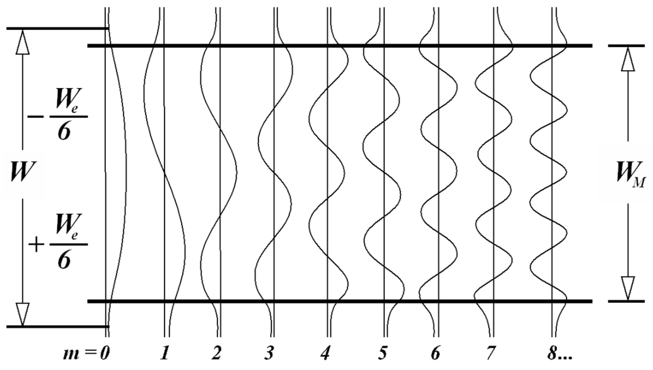
The waveguide supports m lateral modes with mode numbers v = 0, 1, 2, …, (m − 1) at a wavelength in free space (λ0) can be seen in Figure 2.
The operational mechanism of the proposed nanodevices is rooted in the Self-Imaging Principle. Figure 2 illustrates the electric field intensity profile throughout the multimode interference (MMI) region, demonstrating the constructive and destructive interference patterns of the excited guided modes. As depicted in the figure, the optical power distribution periodically converges at specific longitudinal coordinates to form single or multiple replicas of the input field. The precise identification of these focalization points is critical for determining the optimal positioning of the output ports and the overall MMI length. Within this framework, Figure 2 serves not only to validate the modal propagation theory but also to define the spatial search domain for the machine learning algorithm, ensuring maximum power transfer efficiency across the targeted telecommunication bands.
The propagation constant β v and the lateral wavenumber k y v are related to the guiding region index by the dispersion equation:
k y v 2 + β v 2 = k 0 2 n e f f 2                   o n d e   k 0 = 2 π λ 0         e       k y v = ( v + 1 ) π W e v
Thus, the propagation constant β v can be expressed as follows:
β v = k 0 n e f f ( v + 1 ) 2 π λ 4 n e f f W e v 2
The difference between the propagation constants of the fundamental mode ( β 0 ) and the next mode ( β v ) is given by:
β 0 β v = 3 π λ 4 n e f f W e v 2
The beat length in the propagation direction is given by definition as follows:
L π = π β 0 β v
However, we can rewrite β 0 β 1 as:
β 0 β 1 = π v ( v + 2 ) 3 L π  
constituting the phase factor for the formation of selfie-images.
The distribution of the input field, at z = 0, when all modes are considered, and the field profile Ψ(y,0) is contained entirely within the effective width Wev is given by:
Ψ v ( y , L M M I ) = v = 0 m 1 c v ψ v ( y ) e j ( π v ( v + 2 ) 3 L π L M M I )
The form of Ψ(y, LMMI), and consequently the types of images formed, will be determined by the modal excitation cv, and the properties of the phase factor mode. Thus, the field Ψ(y, LMMI) will be a self-image of the input field Ψ(y,0).

3. Artificial Neural Network

Artificial Neural Networks are adaptive computational systems based on mathematical models, which have distributed parallel systems formed by simple processing units (nodes) that calculate certain mathematical functions, normally non-linear [65]. Such units are arranged in one or more layers and interconnected by a large number of connections, generally unidirectional, seeking to simulate the functioning of biological neural networks, inspired by a physical structure designed by nature: the human brain, due to its information processing characteristics and the particularities of interconnections [66,67].

3.1. Multilayer Perceptron

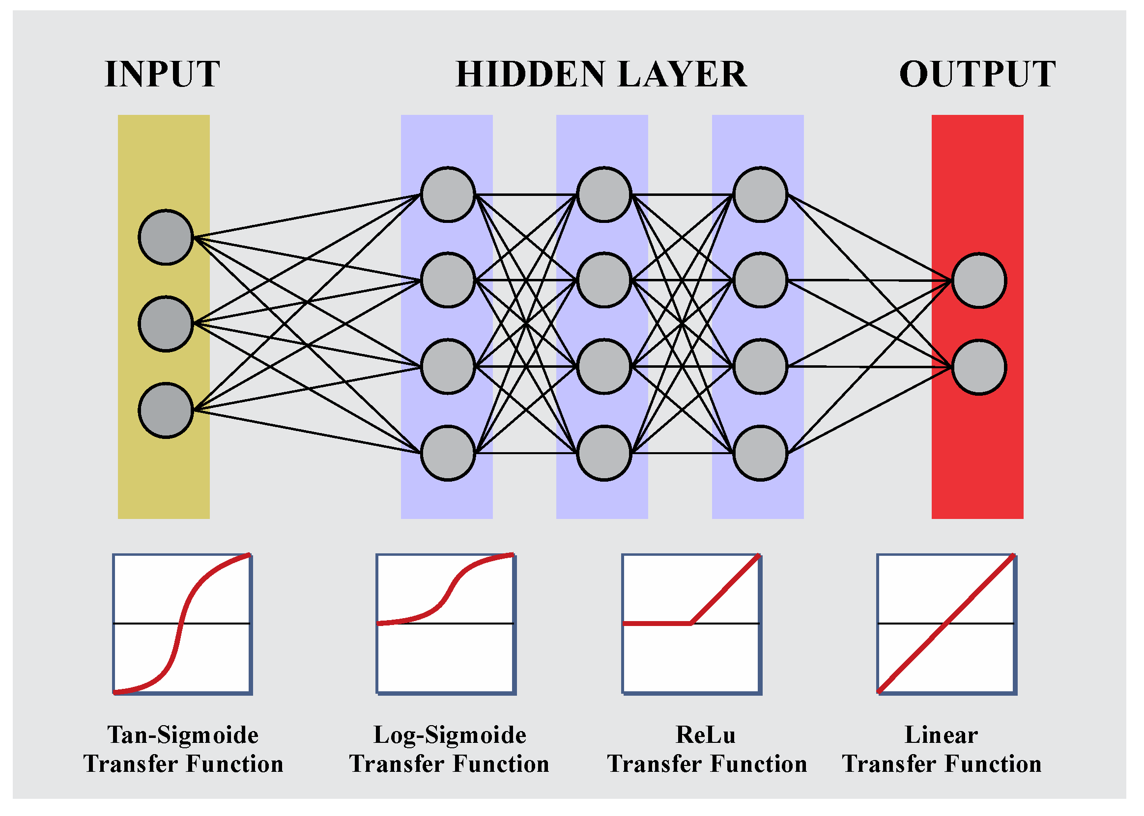
The Multilayer Perceptron (MLP) network is considered an attractive alternative to an empirical formula, as it imitates the non-linear relationship between input and output variables in a more simplified way according Figure 3. The model aims to obtain optimized network weights using a training algorithm designed to minimize the error between the output and target variables by modifying the mutually connected weights [68].

3.2. Supervised Training

Training is the basis of how an ANN works, in which a series of patterns and their respective responses are inserted into the network. In this way, the network is able to learn from examples, make interpolations, and extrapolations of what it has learned. Supervised training of an ANN basically consists of presenting input-output pairs to the network, calculating the outputs depending on the inputs, calculating the error between the desired output and the calculated output, and changing the synaptic values using some type of algorithm. The ANN training process using this algorithm calculates the backpropagation of errors from the outputs towards the inputs, through an error correction mechanism, and weight adjustments of the intermediate layers of the network through training. Training can be done per season, where the entire training set used is presented to the network, and only after that are the synapses updated [69].

3.3. Backpropagation

Backpropagation is an algorithm used in supervised learning, through a mechanism for correcting errors and adjusting the weights of intermediate layers in the network through training. Training takes place in two phases, forward and backward. The forward phase is used to define the network output for a given input pattern. The backward phase takes advantage of the desired output and the output provided by the network to update the weights of the connections [66,69].

4. Results

To generate training data, the numerical beam propagation method was used. To develop, train, test, and validate various Artificial Neural Network architectures, MATLAB R2025b was chosen. The computer used in this work has a Processor 12th Gen Intel® Core™ i7-1255U, 1.70 GHz, and RAM 16.0 Gb.
The training dataset was generated through numerical optical simulations using the Beam Propagation Method (BPM). This method was chosen because it offers a reliable approximation of multimode interference behavior with significantly lower computational cost, while maintaining accuracy for the fundamental transverse-electric (TE) mode in silicon-based waveguides. A total of 6000 input/output data pairs were generated to cover a range of device configurations, and the geometric and optical parameters were systematically varied within the following ranges, as shown in Table 2.
Each simulation outputs the x-axis coordinates (output port position) and y-axis coordinates (MMI region length) corresponding to the maximum power transfer efficiency. The resulting dataset was normalized to the interval [−1, 1] in the ANN configuration and divided into 70% for training, 15% for validation, and 15% for testing, ensuring consistent parameter space coverage and robust generalization, thus ensuring that the neural networks were trained with synthetic data derived from controlled optical simulations, with parameter ranges aligned with practical manufacturing limits and the main telecommunications bands (E, S, C, and L).
The simulations are distributed among eight parameters for 1 × 2 device, nine parameters for 1 × 3 devices and ten parameters for 1 × 4 devices: wavelength (λ), width (WMMI), length (LMMI), core refractive index (nSilicon), substrate refractive index (nSilica), coordinate for the x1-axis, and coordinate for the x2-axis and losses (dB) at the device output.
To ensure the reproducibility of the proposed approach, the complete set of training hyperparameters used in the development of the ANNs, as shown in Table 3, was implemented and trained using the MATLAB Neural Network, widely adopted in supervised learning applications in scientific research. The dataset used for training consisted of 6000 input/output pairs derived from optical simulations based on the Beam Propagation Method (BPM). The training procedure adopted the following configuration parameters, summarized in Table 4, defined after empirical analysis and validation using the k-fold cross-validation method (k = 10).
Critical hyperparameters such as the number of neurons per layer, learning rate, and activation functions were empirically adjusted by observing error convergence curves and regression coefficients (R2). For each configuration tested, three performance indicators were considered: cross-validation mean squared error (MSE), training time, and regression coefficient (R) between predicted outputs and target outputs.
The choice of the Levenberg-Marquardt optimizer was based on its superior convergence speed and stability in medium-sized datasets, typical in optical modeling problems. Networks with Tansig activation in all hidden layers achieved the best generalization performance, presenting MSE ≈ 10−6 and R ≈ 0.99999, confirming strong agreement between predicted and simulated BPM values.
The designed devices are composed of a silicon (Si) core, a silicon dioxide (SiO2) substrate, with a thickness of 0.220 μm, refractive indices of the core (3.476) and substrate (1.444) at the wavelength of 1.550 μm, and an effective refractive index (neff) of 2.848, according to Table 4.
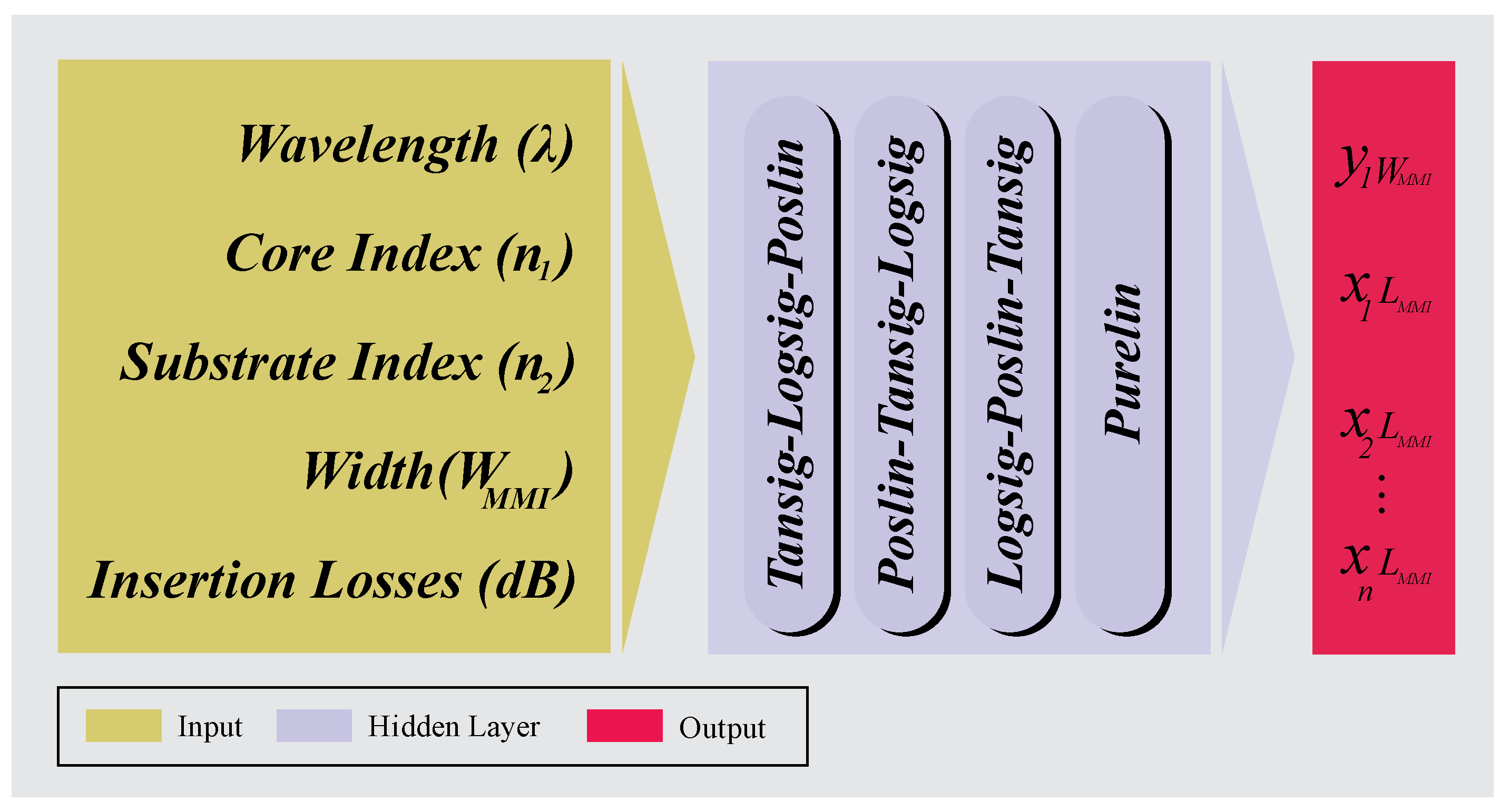
The ANN’s architectures were configured with three hidden layers, alternated with the activation functions Tansig (hyperbolic tangent), Logsig (sigmoid), and Poslin (ReLu—Rectified Linear Unit), and in the output layer, the Purelin function (linear), as can be seen in Figure 4. Each ANN was trained with [ten, eight, and five] and [five, eight, and ten] neurons in the respective layers.
The ANNs were trained using the cross-validation method using the k-fold technique for k-10. The input data was divided into 10 k data blocks, where each training step, the algorithm uses all data blocks for training except one (k-1), then evaluates the model with the data block that was not used for training.
The ANN was configured with five input parameters: wavelength (λ), core refractive index (n1), substrate refractive index (n2), width (WMMI), and efficiency (%). As the aim is to develop an algorithm that establishes a relationship between the input parameters and the geometric characteristics, the network targets were defined as the position on the x-axis that comprises the range of the width (WMMI) and the cut-off length on the y-axis (LMMI), thus providing output port position and MMI region length (x and y coordinates) of the device that provides the signal output with the greatest efficiency.
With the developed algorithm, it was possible to train three ANNs, which presented excellent performance considering the Mean Squared Error (MSE) and low computational cost. After obtaining the coordinates (x, y) provided by the ANNs, new devices were simulated, without compromising power transmission efficiency and with good manufacturing tolerance, using commercial software.
Table 5 presents the three neural networks that showed the best performance. The Tansig activation function is a hyperbolic sigmoidal function with mainly nonlinear characteristics, ideal for capturing continuous variations in data. This function demonstrated a significant contribution to the presented proposal, with its architecture presenting the best performance, with the lowest mean square error of 4.2742 × 10⁻⁶ and linear regression of 0.999997, in addition to a moderate computational time of 7.46 s. The success of Tansig in all hidden layers demonstrates its ability to represent complex and continuous relationships between optical parameters and geometric coordinates for the output port position and MMI region length. In this case, the nature of the function favored learning for regression problems. The function in question is the most relevant in the study, indicating that capturing the nonlinearity of the problem described between optical and geometric behavior is essential to accurately predict device performance.
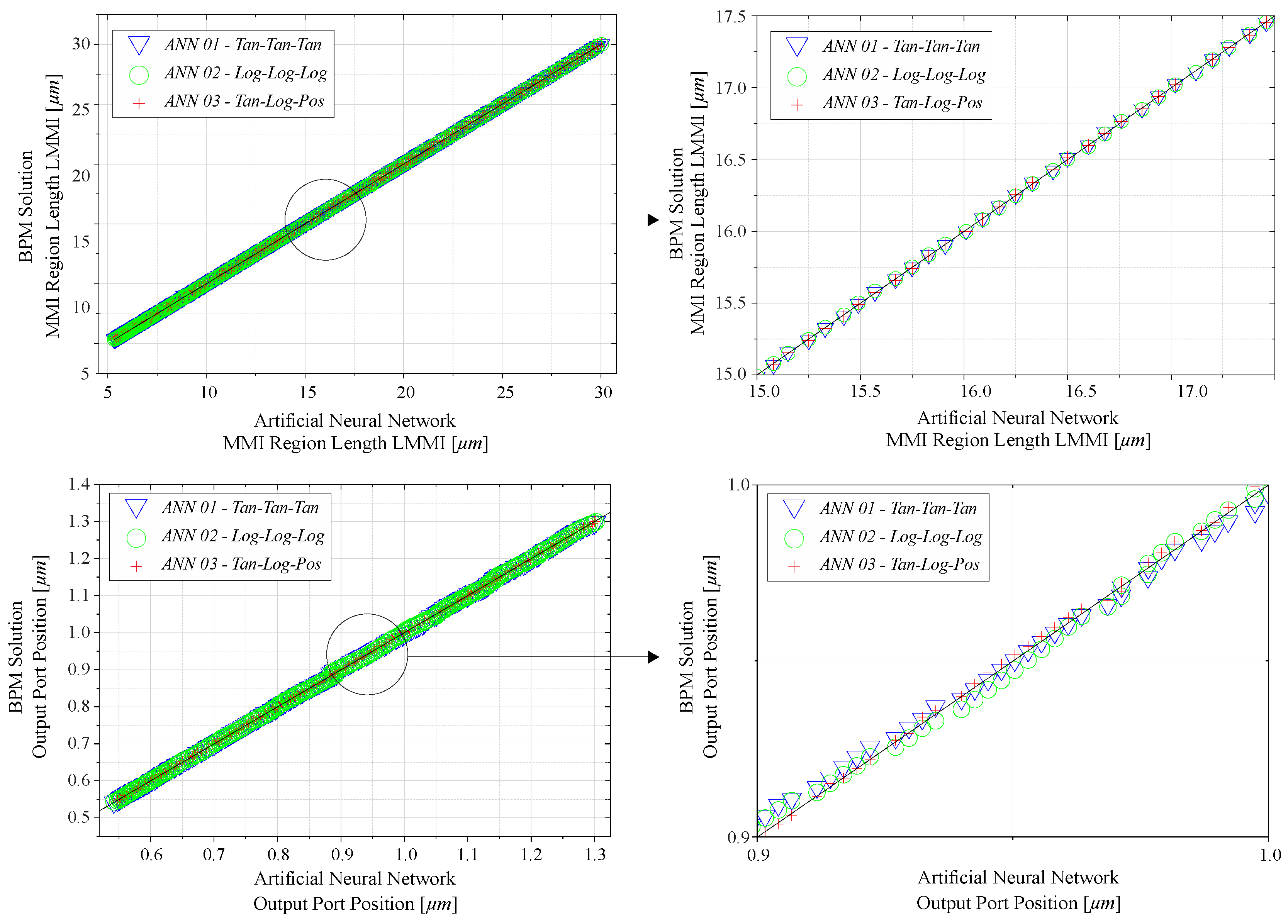
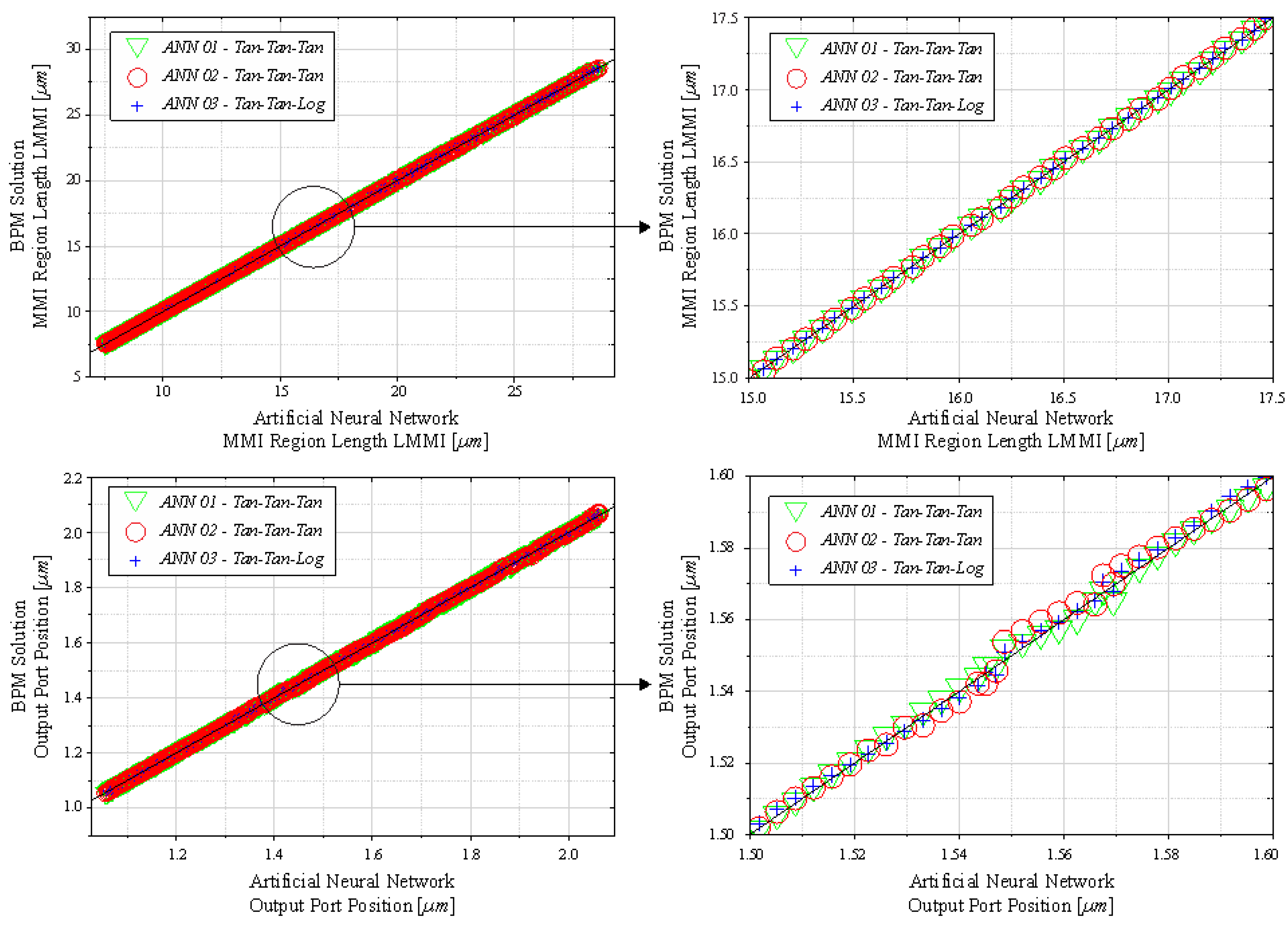
Figure 5 represents the linear regression referring to the results presented by ANN 01, 02, and 03 networks when compared with the BPM Solution response of the waveguide. While the graph on the left represents the position of the output port for the optical signal output, the graph on the right indicates the length of the MMI device, indicating the LMMI.
The linear regression represented in Figure 5 provides a crucial tool for validating the predictive performance of the ANN. The proximity of the data points to the ideal trend line, identified by the black line, demonstrates a strong correlation between the values predicted by the network and the target values provided by the simulation. This result quantifies the accuracy of the model, confirming that the ANN can generalize the physical behavior of the device with high fidelity, capturing the fundamental relationship between the design parameters and the desired optical response.
Table 6 presents information about the devices simulated using BPM and the devices obtained through the best neural network named ANN 01-Tan-Tan-Tan. Using ANN data, it was possible to simulate four MMI devices (1 × 2).
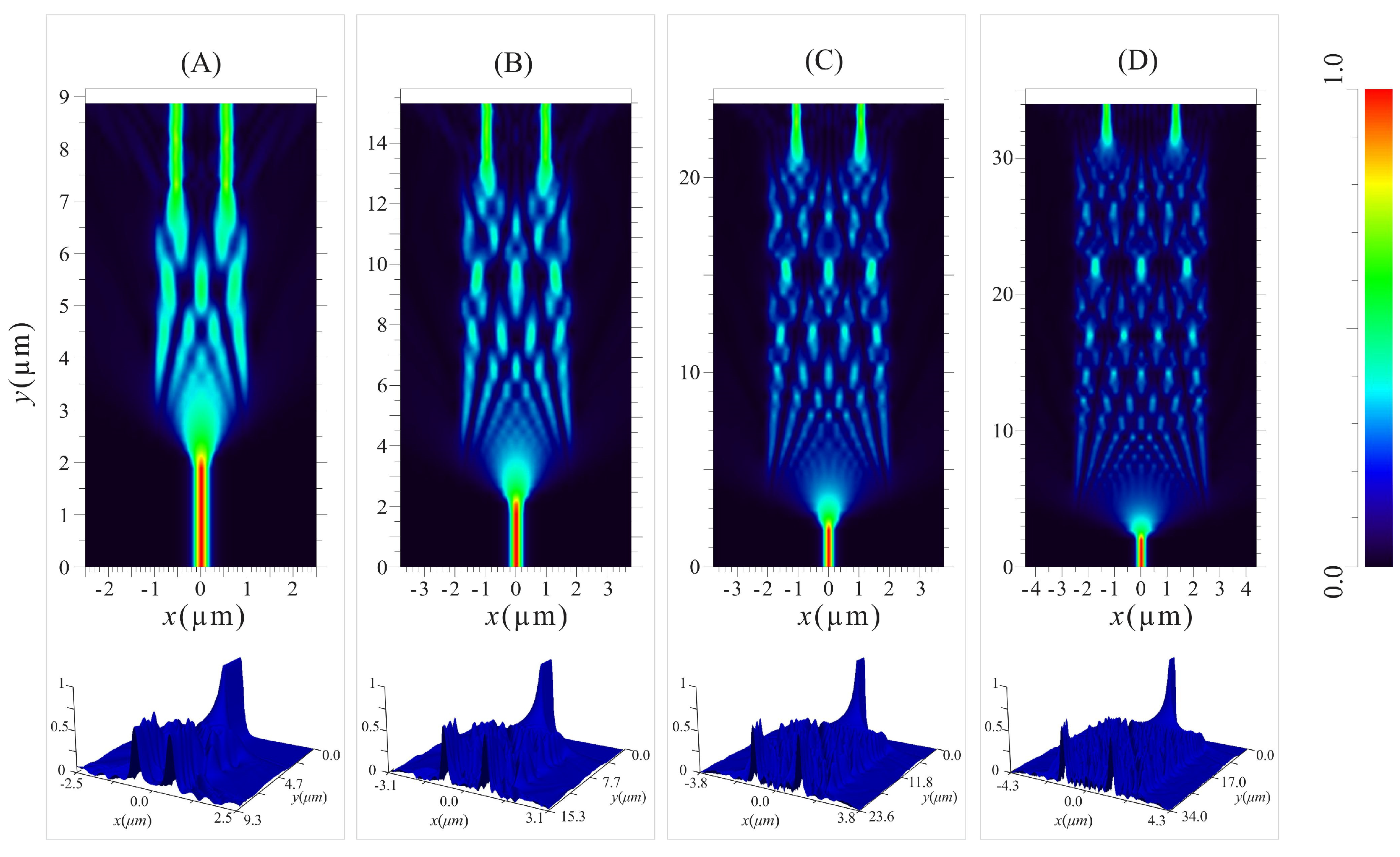
Figure 6A represents the most compact device with a width (WMMI) of 2.00 µm and length (LMMI) measuring 5.3276 µm, computing a difference of 2.4 × 10⁻³ µm in relation to the simulated device with the data obtained through BPM. The coordinates of the x1-axis and x2-axis were −0.5443 and 0.5443 µm, respectively, accounting for a difference of 2.3 × 10⁻³ µm when compared to the simulated device with the data obtained through BPM. With regard to power transfer at the waveguide output, it was calculated that the insertion losses were less than 0.42 dB.
Figure 6D represents the device with the largest dimension among those simulated by ANN, with a width (WMMI) of 5.00 µm and length (LMMI) measuring 29.97 µm, computing a difference of 5.1 × 10⁻² µm in relation to the simulated device with the data obtained through BPM. For this device, the output port position (x1-axis and x2-axis) were −1.2929 and 1.2929 µm, respectively, accounting for a difference of 9.1 × 10⁻³ µm when compared to the simulated device with the data obtained through BPM. Regarding power transfer at the waveguide output, the insertion losses were calculated to be less than 0.68 dB.
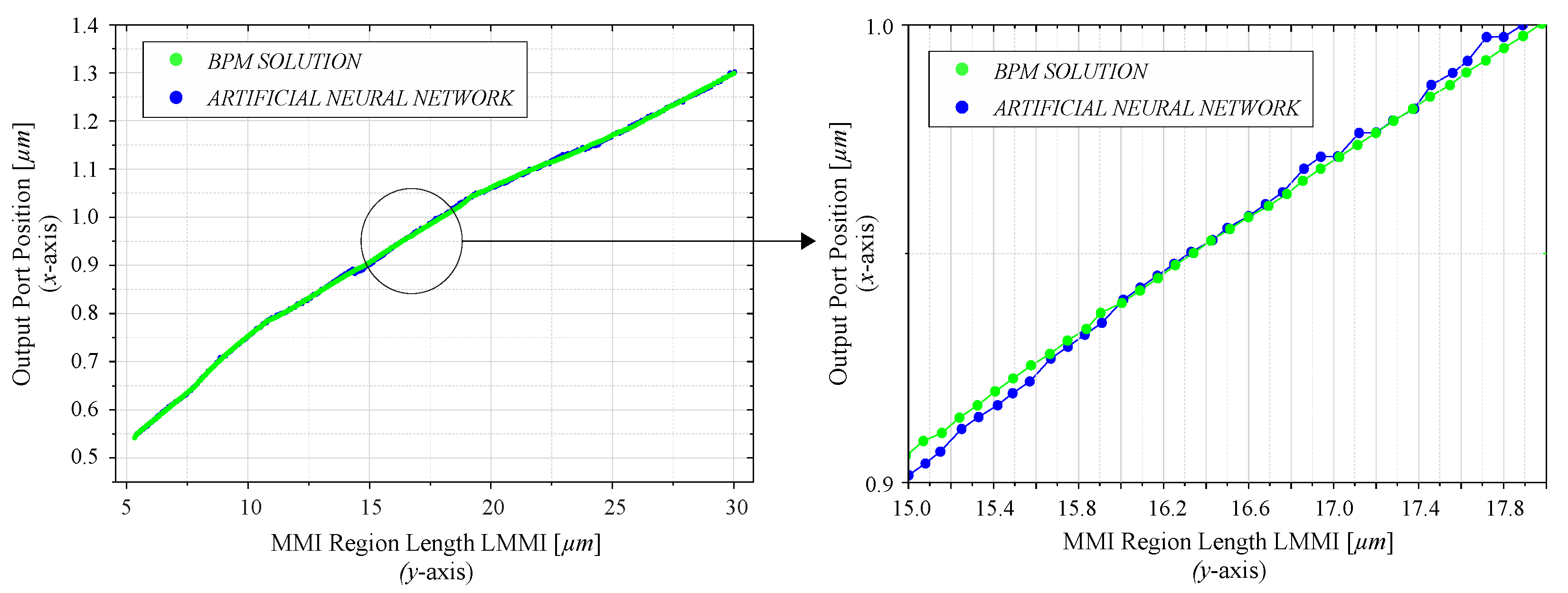
Figure 7 presents a comparison between the simulated device with the data obtained through BPM and the data obtained through the Artificial Neural Network with the best performance among the networks developed. The graph shows the points of the black triangle (output port position and LMMI equivalent to x and y coordinates referring to the analytical data) on the white triangle (output port position and LMMI equivalent to x and y coordinates) obtained by ANN 01-Tan-Tan-Tan), indicating a very small difference, accounting for the smallest and largest difference between the x-axes of 2.46 × 10⁻⁵ and 1.17 × 10⁻² µm respectively, and for the y-axes of 8.96 × 10⁻⁵ and 1.00 × 10⁻² µm, respectively.
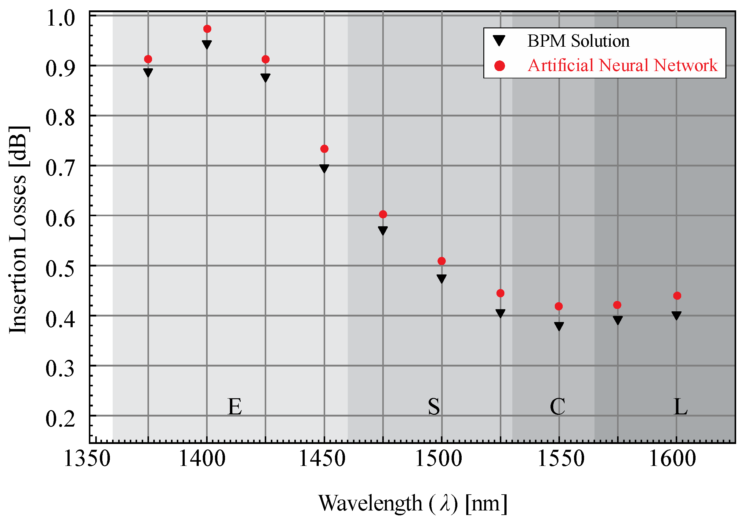
Figure 8 compares the optical power transfer efficiency between a device with a width (WMMI) of 2.20 µm simulated with BPM and a device with the same width simulated with data from ANN 01-Tan-Tan-Tan. The efficiency was calculated for the length range between 1350 and 1600 nm, covering the E, S, C, and L communication bands, showing insertion losses of 0.42 dB for the device simulated using the BPM and insertion losses of 0.38 dB for the device simulated by the algorithm developed using ANN at 1550 nm wavelength and an intrinsic loss of 0.04 dB.
Table 7 presents the three neural networks that showed the best performance. The Tansig activation function is a hyperbolic sigmoidal function with mainly nonlinear characteristics, ideal for capturing continuous variations in data. This function demonstrated a significant contribution to the presented proposal, with its architecture presenting the best performance, with the lowest mean square error of 1.7932 × 10⁻⁶ and linear regression of 0.999998, in addition to a moderate computational time of 37.03 s. The success of Tansig in all hidden layers demonstrates its ability to represent complex and continuous relationships between optical parameters and geometric coordinates for the output port position and LMMI. In this case, the nature of the function favored learning for regression problems. The function in question is the most relevant in the study, indicating that capturing the nonlinearity of the problem described between optical and geometric behavior is essential to accurately predict device performance.
Logsig is another sigmoidal activation function and is usually effective when the data are normalized in this range. This function performed well, with an MSE of 4.0136 × 10⁻⁶ and a regression of 0.999996, but with a significantly higher computational time of 87.93 s. Logsig was less effective than Tansig in synthesizing the complexity of the problem, perhaps due to its asymmetry with respect to zero, which may limit the modeling of variations centered at this point. The activation function in question proved to be adequate, but less efficient, both in accuracy and computational cost. Its nature in some cases may compromise the identification of patterns where the data present variation centered around zero.
Poslin (Positive Linear Transfer Function) returns zero for negative inputs and a direct value for positive inputs. It is a piecewise linear function, similar to a ReLU without the negative part. Although the ANN C architecture is mixed, the use of Poslin in the third layer resulted in a lower performance in terms of MSE (4.2742 × 10⁻⁶), although presenting a satisfactory result. In the linear function condition, Poslin does not contribute as expected to solve the issue of nonlinearity required for the complexity of the presented problem, which may have limited the capacity of this network due to the configured architecture. The presence of Poslin decreased the expressiveness of the network in problems that require deeper nonlinear modeling; however, it was useful to reduce the complexity of the problem and accelerate training at the expense of a small loss of accuracy, as can be observed in the computational time of 26.34 s.
Figure 9 represents the linear regression referring to the results presented by ANN A, B, and C networks when compared with the BPM solution response of the waveguide. While the graph on the left represents the position of the output port (x-axis coordinate) for the optical signal output, the graph on the right indicates the length of the MMI device, indicating the LMMI (y-axis coordinate).
The high clustering of data around the line and the coefficient of determination (R2) close to unity attest to the strong correlation between the values predicted by the network and the simulation data. This result validates the ANN’s ability to accurately capture the functional relationship between geometric parameters and optical response.
According to Table 8, the difference between the analytically simulated device and the device with the coordinates provided by the trained ANN shows a difference of less than 1.0 nanometer for the x1 and x3-axis and of less than 0.5 nanometer for the x2-axis coordinates, and for the y-axis coordinates, a difference of 3.1 nanometer at the cutoff limit for higher power coupling. it was possible to simulate four MMI devices (1 × 3).
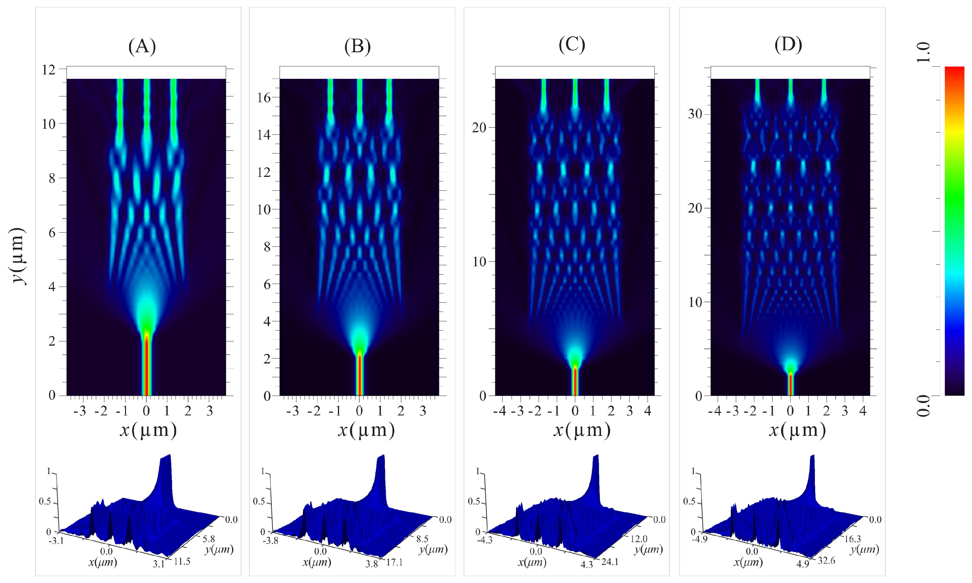
The self-images of the electromagnetic field and solid model produced by the 1 × 3 MMI device can be seen in Figure 10, which was designed based on data generated by the Artificial Neural Network (ANN A-Tan-Tan-Tan) using the Tansig activation function in the three hidden layers, and shows the propagation of light along the LMMI (y-axis) of the waveguide. It is then possible to observe the formation of three intensity maxima at the output, revealing the expected condition of a correctly designed 1 × 3 nanodevice.
Figure 10A represents the most compact device with a width (WMMI) of 3.00 µm and length (LMMI) measuring 7.545 µm, computing a difference of 5 × 10⁻³ µm in relation to the device simulated with the data obtained through BPM. The coordinates of the x1-axis, x2-axis, and x3-axis were −1.054, 1.4 × 10⁻³, and 1.054 µm, respectively, accounting for a difference of 2 × 10⁻³ µm for the output port position (x1-axis and x3-axis coordinates) when compared to the simulated device with the data obtained through BPM. With regard to power transfer at the waveguide output, it was calculated with insertion losses of less than 0.37 dB.
Figure 10D represents the device with the largest dimension among those simulated by ANN, with a width (WMMI) of 6.00 µm and length (LMMI) measuring 28.579 µm, computing a difference of 1 × 10⁻³ µm in relation to the simulated device with the data obtained through BPM. For this device, the coordinates of the x1-axis, x2-axis, and x3-axis were −2.059, 2.0 × 10⁻³, and 2.059 µm, respectively, accounting for a difference of 2 × 10⁻³ µm for the x1-axis and x3-axis coordinates when compared to the simulated device with the data obtained through BPM. Regarding power transfer at the waveguide output, it was calculated with an insertion loss of less than 0.58 dB.
The result indicates that ANN A was able to model with high precision the relationship between the input parameters given by the refractive index, width and length of the guide and the ideal geometric coordinates (x, y) to maximize the efficiency of the device, thus experimentally validating the predictions of the network in question by clearly defining the eigenimage, proving that the predicted coordinates for WMMI and LMMI result in an efficient and symmetrical power division and that the geometric structure provided by the network is in accordance with the physical behavior predicted by the multimodal interference relations.
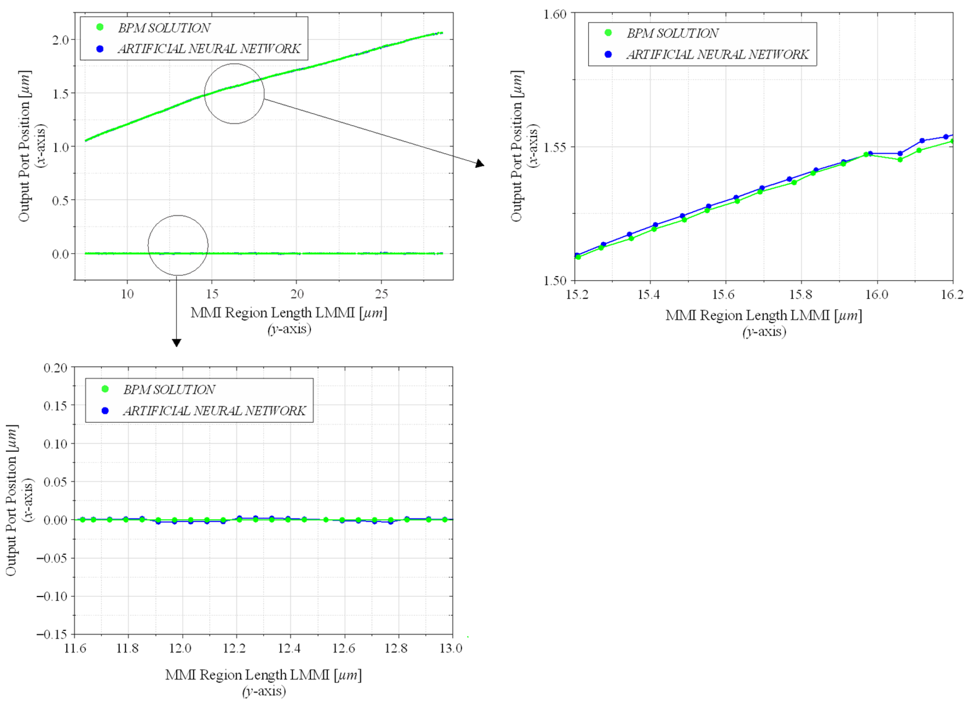
Figure 11 shows a comparison between the output port position and MMI region length (x, y coordinates) of the analytically simulated devices and the devices designed by the ANN. The overlapping points indicate a very small difference, with a loss of less than 0.38 dB.
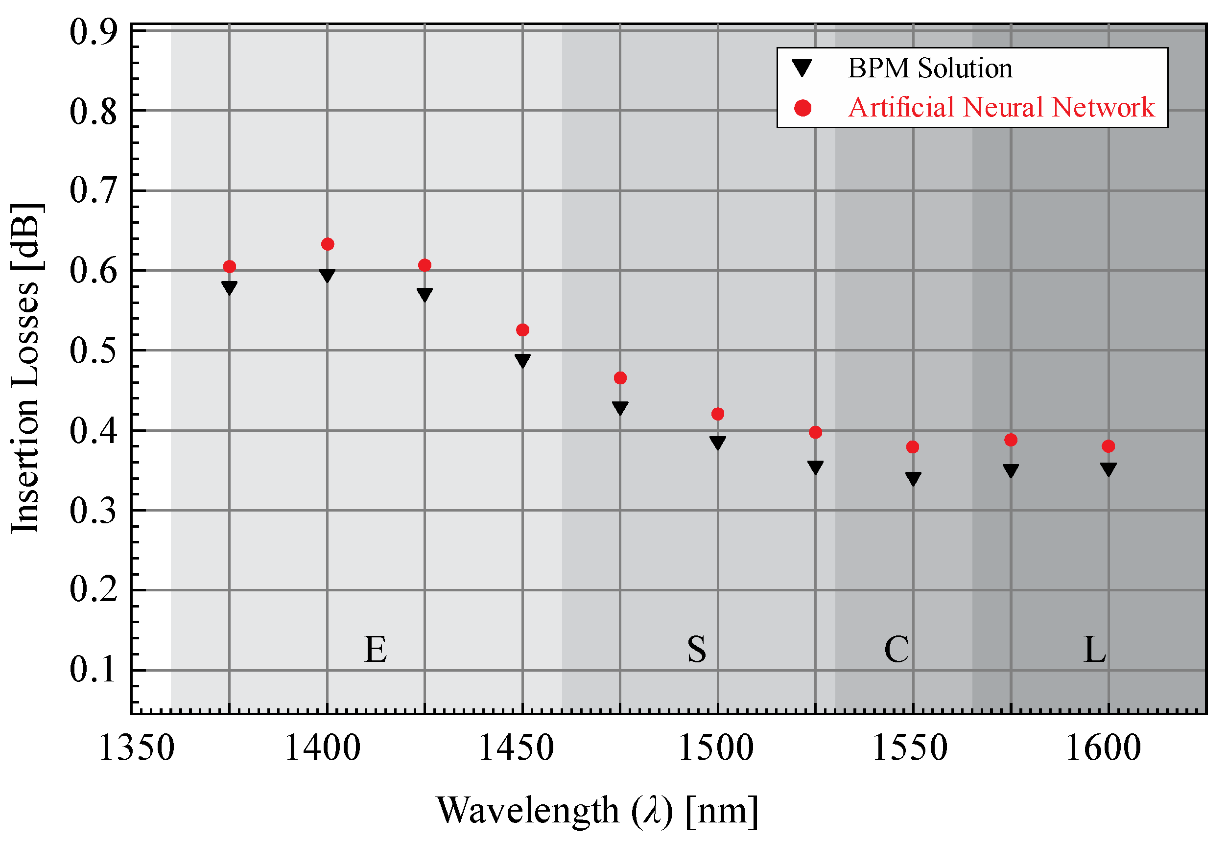
Figure 12 compares the efficiency of optical power transfer between a device that presented the best power transfer width (WMMI) of 3.08 µm, simulated by BPM, and a device with the same characteristics, but simulated with data from ANN A-Tan-Tan-Tan. The efficiency was calculated for the wavelength range between 1350 and 1600 nm, covering the communication bands E, S, C, and L, presenting insertion losses of 0.34 dB for the simulated by BPM device and insertion losses of 0.38 dB for the device simulated by the algorithm developed using ANN at 1550 nm wavelength and an intrinsic loss of 0.04 dB. From reading the graph, it can be concluded that the communication bands that offer the best responses to MMI devices with the characteristics presented are the C-bands.
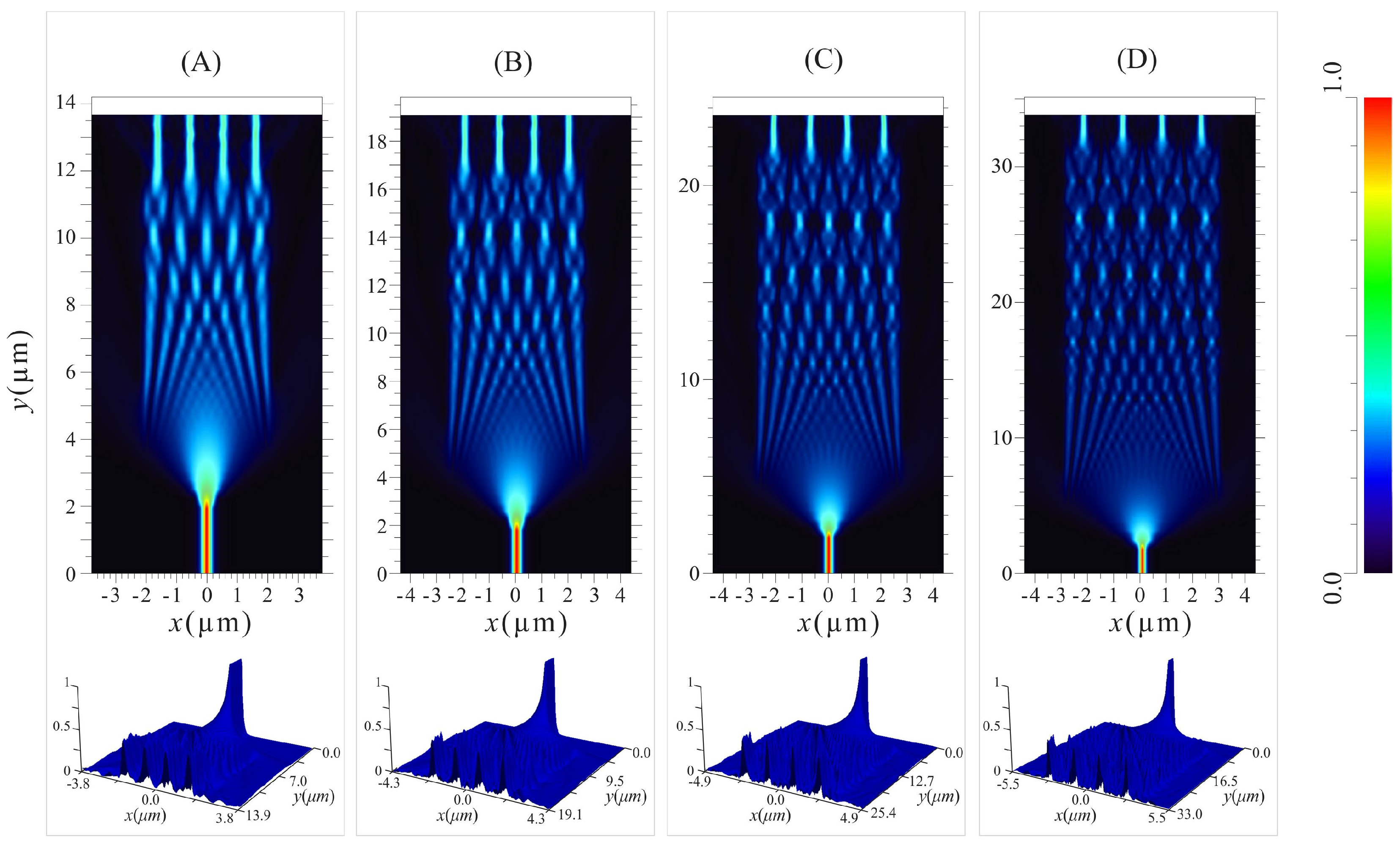
The self-images of the electromagnetic field and solid model produced by the 1 × 4 MMI device can be seen in Figure 13, which was designed based on data generated by the Artificial Neural Network (ANN A-Tan-Tan-Tan) using the Tansig activation function in the three hidden layers, and shows the propagation of light along the MMI region length (y-axis) of the waveguide. It is then possible to observe the formation of four intensity maxima at the output, revealing the expected condition of a correctly designed 1 × 4 nanodevice.
Figure 13A represents the most compact device with a width (WMMI) of 4.00 µm and length (LMMI) measuring 9.93 µm, computing a difference of 4.3 × 10⁻³ µm in relation to the device simulated with the data obtained through BPM. The coordinates of the x1-axis, x2-axis, x3-axis, and x4-axis were −1.556, −0.528, 1.556, and 0.528 µm, respectively. With regard to the power transfer at the waveguide output, it was calculated with insertion losses of less than 0.42 dB.
Figure 13D represents the device with the largest dimension among those simulated by ANN, with a width (WMMI) of 7.00 µm and length (LMMI) measuring 28.97 µm, computing a difference of 1,4 × 10⁻³ µm in relation to the simulated device with the data obtained through BPM. For this device, the output port position (x1-axis, x2-axis, x3-axis, and x4-axis coordinates) were −2.681, −0.895, 2.681, and 0.895 µm. Regarding power transfer at the waveguide output, it was calculated with an insertion loss of less than 0.59 dB.
Table 9 presents the results, revealing that the choice of activation function significantly impacts the accuracy, computational cost, and generalization capacity of the network. Tansig stands out as the most suitable for modeling the complex nonlinear optical phenomena present in the design of MMI devices.
For this work, in addition to insertion loss, the uniformity of power distribution between output ports is a performance metric for any power divider. The MMI devices (1 × 2, 1 × 3, and 1 × 4) using the geometries predicted by the ANN were designed so that the power imbalance between output ports would be uniform across the entire operating bandwidth. Thus, combined with the previously reported low insertion losses (ranging from 0.34 dB to 0.68 dB), it confirms that the devices achieve efficient and balanced power division. It is important to note that the reported insertion losses include the intrinsic loss inherent to the multimode interference phenomenon, which was calculated at approximately 0.04 dB for the fundamental mode in the simulated structures. Therefore, the demonstrated performance comprehensively validates the inverse design capability of the ANN, producing devices that meet the key parameters for practical application in photonic integrated circuits.
The practical implementation of photonic devices, especially at the nanoscale, is intrinsically linked to the variations inherent in nanofabrication processes. Therefore, a thorough tolerance analysis is not merely supplementary but a fundamental step in evaluating the robustness and feasibility of a proposed design. This analysis allows the identification of critical parameters whose control is essential to maintain device performance, predict yield rates, and guide the specification of fabrication requirements.
This work performed a systematic tolerance analysis for the designed 1 × 2 and 1 × 3 Multimode Interference (MMI) power dividers. A realistic fabrication variation range of 10 nanometers (0.01 µm) was adopted as a reference. This value is consistent with the precision limits of modern lithography processes used in silicon photonics. Based on the results presented in Table 10, the inverse design methodology with ANN proves valuable for managing tolerances, as it can predict optimal configurations that compensate for known or expected variations in the manufacturing process, especially for the most critical parameters identified in this analysis.
Table 11 provides a comparative analysis between the Beam Propagation Method (BPM) simulations and some optimization methods for power splitters. These results validate the efficacy of the multilayer perceptron architecture in bypassing computationally expensive iterative simulations, establishing a robust framework for the development of ultra-compact photonic integrated circuits across the E, S, C, and L telecommunication bands.
The comparison shows that the proposed ANN-based strategy substantially reduces the computational cost of the inverse design process. The ANN provides optimal coordinates in fractions of a second without compromising optical efficiency. For applications where fast iteration and low design latency are essential, the ANN demonstrates an operational advantage.

5. Conclusions

Using modeling capabilities for MMI device design through Machine Learning techniques with k-fold cross-validation (k = 10) demonstrated the ability of AI algorithms to learn the complex relationships between compact structures and their associated optical responses, thus providing a solution capable of solving complex inverse design problems. The trained neural network achieved remarkable accuracy with the lowest mean square error of 4.2742 × 10⁻⁶ and a linear regression of 0.999997, in addition to a moderate computational time of 7.46 s for the 1 × 2 device with insertion losses between 0.42 and 0.68 dB; and the lowest mean square error of 1.7932 × 10⁻⁶ and a linear regression of 0.999998, in addition to a moderate computational time of 37.03 s for the 1 × 3 device with insertion losses between 0.37 and 0.58 dB at 1550 nm wavelength, both designed with the Tansig activation function.
Several important improvements would enhance the applicability of the methodology presented in this work. The most significant would be increasing the design’s robustness to handle process variations in photolithography, which would enable high-throughput manufacturing. This research has demonstrated the development of MMI device models with efficient transmission, low insertion losses, and results compatible with commonly designed and commercially manufactured MMI devices. Thus, it can be concluded that the presented approach demonstrates high accuracy for waveguide design prediction using Artificial Neural Networks and that the proposed methodology can be adapted and applied to the analysis and design of various complex integrated photonic nanodevices.

Author Contributions

Conceptualization, R.d.M.C., A.D.S. and V.F.R.-E.; methodology, R.d.M.C., A.D.S. and V.F.R.-E.; writing—original draft preparation, R.d.M.C., A.D.S. and V.F.R.-E.; formal analysis, R.d.M.C., A.D.S. and V.F.R.-E.; writing—review and editing, R.d.M.C., A.D.S. and V.F.R.-E.; funding acquisition, R.d.M.C., A.D.S. and V.F.R.-E. All authors have read and agreed to the published version of the manuscript.

Funding

This work was supported by CNPq (303795/2022-0 and 407612/2025-4), CAPES (88887.026668/2024-00), and FAPESB (TO PIE 0003/2022).

Data Availability Statement

Data will be made available on request.

Conflicts of Interest

The authors declare no conflicts of interest. The funders had no role in the design of the study; in the collection, analyses, or interpretation of data; in the writing of the manuscript; or in the decision to publish the results.

References

  1. Liu, F.; Lv, H.; Zhang, H.; Liu, S.; Liang, Y.; Wang, H.; Cong, Y.; Li, X.; Guo, Q. Design of Polarization-Independent 1 × 2 Optical Power Splitter Based on Silicon Nitride Slot Waveguide Structure. Sci. Rep. 2025, 15, 25288. [Google Scholar] [CrossRef] [Scilit]
  2. Vakarin, V.; Melati, D.; Dinh, T.T.D.; Le Roux, X.; Kan, W.K.K.; Dupré, C.; Szelag, B.; Monfray, S.; Boeuf, F.; Cheben, P.; et al. Metamaterial-Engineered Silicon Beam Splitter Fabricated with Deep UV Immersion Lithography. Nanomaterials 2021, 11, 2949. [Google Scholar] [CrossRef] [Scilit]
  3. Su, Y.; Chen, H.; Zang, Y.; Hao, Q.; Ma, Y.; Tong, Y. Machine Learning-Assisted Design Automation of Integrated Photonic Devices. In Proceedings of the 2025 International Symposium of Electronics Design Automation (ISEDA), Hong Kong, China, 9–12 May 2025; IEEE: Hong Kong, China, 2025; pp. 718–723. [Google Scholar]
  4. Alam, M.K.; Afsary, N.; Sikder, S.; Parvez, S.; Roy, P.; Faruk Rasel, M.O. Near-Infrared Y-Branch Polymer Splitters Realized with Compact MMI Structures for Efficient Power Splitting. Opt. Contin. 2024, 3, 413. [Google Scholar] [CrossRef] [Scilit]
  5. Zhang, Y.; Wu, X.; He, Z.; Liu, L.; Xu, L. Compact Asymmetric 1 × 2 Multimode Interference Optical Switch. J. Opt. Pure Appl. Opt. 2009, 11, 105401. [Google Scholar] [CrossRef] [Scilit]
  6. Silva-Santos, C.H.; Rodríguez-Esquerre, V.F.; Hernández-Figueroa, H.E. Artificial Immune Network Design of Optical Multiplexers/Demultiplexers. J. Microw. Optoelectron. Electromagn. Appl. 2015, 14, 229–237. [Google Scholar] [CrossRef] [Scilit]
  7. Isakov, O.; Frishman, A.; Malka, D. Data Center Four-Channel Multimode Interference Multiplexer Using Silicon Nitride Technology. Nanomaterials 2024, 14, 486. [Google Scholar] [CrossRef] [Scilit]
  8. Sun, C.; Yu, Y.; Ye, M.; Chen, G.; Zhang, X. An Ultra-Low Crosstalk and Broadband Two-Mode (de)Multiplexer Based on Adiabatic Couplers. Sci. Rep. 2016, 6, 38494. [Google Scholar] [CrossRef] [Scilit] [PubMed]
  9. Amanti, F.; Andrini, G.; Armani, F.; Barbato, F.; Bellani, V.; Bonaiuto, V.; Cammarata, S.; Campostrini, M.; Dao, T.H.; De Matteis, F.; et al. Integrated Photonic Passive Building Blocks on Silicon-on-Insulator Platform. Photonics 2024, 11, 494. [Google Scholar] [CrossRef] [Scilit]
  10. Earnshaw, M.P.; Soole, J.B.D.; Cappuzzo, M.; Gomez, L.; Laskowski, E.; Paunescu, A. 8 × 8 Optical Switch Matrix Using Generalized Mach-Zehnder Interferometers. IEEE Photonics Technol. Lett. 2003, 15, 810–812. [Google Scholar] [CrossRef] [Scilit]
  11. Kalavrouziotis, D.; Papaioannou, S.; Vyrsokinos, K.; Markey, L.; Dereux, A.; Giannoulis, G.; Apostolopoulos, D.; Avramopoulos, H.; Pleros, N. Demonstration of a Plasmonic MMI Switch in 10-Gb/s True Data Traffic Conditions. IEEE Photonics Technol. Lett. 2012, 24, 1819–1822. [Google Scholar] [CrossRef] [Scilit]
  12. Ota, M.; Sumimura, A.; Fukuhara, M.; Ishii, Y.; Fukuda, M. Plasmonic-Multimode-Interference-Based Logic Circuit with Simple Phase Adjustment. Sci. Rep. 2016, 6, 24546. [Google Scholar] [CrossRef] [Scilit] [PubMed]
  13. Zhang, L.; Zhu, K.; Yao, Y.; Tian, X.; Xu, H.; Nie, Z. Research Progress in Tunable Fiber Lasers Based on Multimode Interference Filters. Micromachines 2023, 14, 2026. [Google Scholar] [CrossRef] [Scilit]
  14. Liu, S.; Liu, B.; Lv, H.; Liang, Y.; Liu, F.; Wang, H.; Cong, Y.; Li, X.; Guo, Q. Design of a 1 × 3 Power Splitter Based on Multimode Interference in a Parabolic-Type Slot-Waveguide Structure. Appl. Sci. 2024, 14, 5829. [Google Scholar] [CrossRef] [Scilit]
  15. Li, D.; Li, J.; Li, R.; Liu, J. The Design and Characterization of an Ultra-Compact Asymmetrical Multimode Interference Splitter on Lithium Niobate Thin Film. Photonics 2024, 11, 60. [Google Scholar] [CrossRef] [Scilit]
  16. Liang, Y.; Lv, H.; Liu, B.; Wang, H.; Liu, F.; Liu, S.; Cong, Y.; Li, X.; Guo, Q. Compact Low Loss Ribbed Asymmetric Multimode Interference Power Splitter. Photonics 2024, 11, 472. [Google Scholar] [CrossRef] [Scilit]
  17. Xu, L.; Wang, Y.; El-Fiky, E.; Mao, D.; Kumar, A.; Xing, Z.; Saber, M.G.; Jacques, M.; Plant, D.V. Compact Broadband Polarization Beam Splitter Based on Multimode Interference Coupler with Internal Photonic Crystal for the SOI Platform. J. Light. Technol. 2019, 37, 1231–1240. [Google Scholar] [CrossRef] [Scilit]
  18. Zhao, W.; Huang, X.; Lu, Z. Demonstration of Super Self-Imaging in Indefinite Anisotropic Metamaterial; Boardman, A.D., Engheta, N., Noginov, M.A., Zheludev, N.I., Eds.; SPIE: San Diego, CA, USA, 2011; p. 80932J. [Google Scholar]
  19. Soldano, L.B.; Pennings, E.C.M. Optical Multi-Mode Interference Devices Based on Self-Imaging: Principles and Applications. J. Light. Technol. 1995, 13, 615–627. [Google Scholar] [CrossRef] [Scilit]
  20. Liang, B.; Xu, D.; Yu, N.; Xu, Y.; Ma, X.; Liu, Q.; Asif, M.S.; Yan, R.; Liu, M. Physics-Guided Neural-Network-Based Inverse Design of a Photonic-Plasmonic Nanodevice for Superfocusing. ACS Appl. Mater. Interfaces 2022, 14, 27397–27404. [Google Scholar] [CrossRef] [Scilit] [PubMed]
  21. Yao, K.; Unni, R.; Zheng, Y. Intelligent Nanophotonics: Merging Photonics and Artificial Intelligence at the Nanoscale. Nanophotonics 2019, 8, 339–366. [Google Scholar] [CrossRef] [Scilit]
  22. Zhang, Q.; Yu, H.; Barbiero, M.; Wang, B.; Gu, M. Artificial Neural Networks Enabled by Nanophotonics. Light. Sci. Appl. 2019, 8, 42. [Google Scholar] [CrossRef] [Scilit]
  23. Hegde, R.S. Deep Learning: A New Tool for Photonic Nanostructure Design. Nanoscale Adv. 2020, 2, 1007–1023. [Google Scholar] [CrossRef] [Scilit]
  24. Chen, H.; Li, N.; Zhao, Y.; Ou, H.; Wang, Y.; Jing, X.; Zhang, N.; Su, Z.; Huang, L. Maximizing the Chirality of Bound States in the Continuum by Inverse Design. Photon. Res. 2025, 13, 2054. [Google Scholar] [CrossRef] [Scilit]
  25. Zhou, H.; Liao, K.; Su, Z.; Li, T.; Geng, G.; Li, J.; Wang, Y.; Hu, X.; Huang, L. Tunable On-Chip Mode Converter Enabled by Inverse Design. Nanophotonics 2023, 12, 1105–1114. [Google Scholar] [CrossRef] [Scilit]
  26. Chen, Z.; Wan, L.; Gao, S.; Zhu, K.; Zhang, M.; Li, Y.; Huang, X.; Li, Z. On-Chip Waveguide Amplifiers for Multi-Band Optical Communications: A Review and Challenge. J. Light. Technol. 2022, 40, 3364–3373. [Google Scholar] [CrossRef] [Scilit]
  27. Guo, W.; Wu, Y.; Xiong, Z.; Jing, Y.; Chen, Y. Simple yet Effective Analysis of Waveguide Mode Symmetry: Generalized Eigenvalue Approach Based on Maxwell’s Equations. Opt. Express 2022, 30, 37910. [Google Scholar] [CrossRef] [Scilit]
  28. Qian, C.; Kaminer, I.; Chen, H. A Guidance to Intelligent Metamaterials and Metamaterials Intelligence. Nat. Commun. 2025, 16, 1154. [Google Scholar] [CrossRef] [Scilit] [PubMed]
  29. Sisnando, A.D.; Esquerre, V.F.R.; Vieira, L.D.F.; Rubio-Mercedes, C.E. Inverse Design of Tapers by Bio-Inspired Algorithms. J. Microw. Optoelectron. Electromagn. Appl. 2020, 19, 39–49. [Google Scholar] [CrossRef] [Scilit]
  30. Cooney, K.; Peters, F.H. Analysis of Multimode Interferometers. Opt. Express 2016, 24, 22481. [Google Scholar] [CrossRef] [Scilit]
  31. Lee, D.L. Electromagnetic Principles of Integrated Optics; John Wiley & Sons: New York, NY, USA, 1986; ISBN 978-0-471-87978-7. [Google Scholar]
  32. Anagnos, T.; Harris, R.J.; Corrigan, M.K.; Reeves, A.P.; Townson, M.J.; MacLachlan, D.G.; Thomson, R.R.; Morris, T.J.; Schwab, C.; Quirrenbach, A. Simulation and Optimisation of an Astrophotonic Reformatter. Mon. Not. R. Astron. Soc. 2018, 478, 4881–4889. [Google Scholar] [CrossRef] [Scilit]
  33. Tasnim, F.; Afsary, N.; Faruk Rasel, M.O.; Ishigure, T. Graded-Index Core-Based Polarization Beam Splitters Realized with Symmetric Polymer Directional Couplers. Opt. Contin. 2023, 2, 1040. [Google Scholar] [CrossRef] [Scilit]
  34. Bouda, M.; Van Uffelen, J.W.M.; Van Dam, C.; Verbeek, B.H. Compact 1 × 16 Power Splitter Based on symmetrical1×2MMI Splitters. Electron. Lett. 1994, 30, 1756–1758. [Google Scholar] [CrossRef] [Scilit]
  35. Leuthold, J.; Hess, R.; Eckner, J.; Besse, P.A.; Melchior, H. Spatial Mode Filters Realized with Multimode Interference Couplers. Opt. Lett. 1996, 21, 836. [Google Scholar] [CrossRef] [Scilit] [PubMed]
  36. Kim, H.K.; Lee, B.K.; Langer, D.W.; Min, D.-S.; Li, C.-C. Waveguide Beamsplitters Integrated with an Erbium-Doped Thin-Film Optical Amplifier; Wang, S.-Y., Park, Y.-S., Eds.; SPIE: San Jose, CA, USA, 1997; p. 268. [Google Scholar] [CrossRef] [Scilit]
  37. Lagali, N.S.; MacDonald, R.I.; Paiam, M.R.; Woerhoff, K.; Driessen, A. Silica-Based Rib Waveguides for Integrated Optics Using Multimode Interference; Lampropoulos, G.A., Lessard, R.A., Eds.; SPIE: Ottawa, Canada, 1998; p. 380. [Google Scholar] [CrossRef] [Scilit]
  38. Chuang, W.C.; Chang, C.Y.; Lai, C.C.; Lin, K.C. Integrated-Optics Multimode-Interference Wavelength Division Multiplexer for Optical Communication. Fiber Integr. Opt. 1999, 18, 93–104. [Google Scholar] [CrossRef] [Scilit]
  39. Das, S.; Geraghty, D.F.; Honkanen, S.; Peyghambarian, N. MMI Splitters by Ion-Exchange in Glass; Righini, G.C., Honkanen, S., Eds.; SPIE: San Jose, CA, USA, 2000; pp. 239–247. [Google Scholar] [CrossRef] [Scilit]
  40. Wei, H.; Yu, J.; Zhang, X.; Liu, Z. Compact 3-dB Tapered Multimode Interference Coupler in Silicon-on-Insulator. Opt. Lett. 2001, 26, 878. [Google Scholar] [CrossRef] [Scilit] [PubMed]
  41. Rooms, F.; Morand, A.; Schanen-Duport, I.; Berger, J.-P.; Benech, P. Design of a Three Telescope Interferometers Using a Multimode Interference Waveguide; Sidorin, Y.S., Tervonen, A., Eds.; SPIE: San Jose, CA, USA, 2002; p. 246. [Google Scholar] [CrossRef] [Scilit]
  42. Masanovic, M.L.; Skogen, E.J.; Barton, J.S.; Sullivan, J.M.; Blumenthal, D.J.; Coldren, L.A. Multimode Interference-Based Two-Stage 1/Spl Times/2 Light Splitter for Compact Photonic Integrated Circuits. IEEE Photonics Technol. Lett. 2003, 15, 706–708. [Google Scholar] [CrossRef] [Scilit]
  43. Wang, W. Design and Fabrication of Multimode Interference Coupler with Strong Confinement Structure on Silicon-on-Insulator. Opt. Eng. 2004, 43, 2495. [Google Scholar] [CrossRef] [Scilit]
  44. Rashed, A.M.; Selviah, D.R. Modeling of a Polymer 1 × 3 MMI Power Splitter for Optical Backplane. In Proceedings of the Conference on Optoelectronic and Microelectronic Materials and Devices, Brisbane, QLD, Australia, 8–10 December 2004; IEEE: Brisbane, Australia, 2004; pp. 281–284. [Google Scholar] [CrossRef] [Scilit]
  45. Ibrahim, M.H.; Kassim, N.M.; Mohammad, A.B.; Chin, M.-K.; Lee, S.-Y. Polymeric Optical Splitter Based on Multimode Interference Mechanism. In Proceedings of the 2006 4th Student Conference on Research and Development, Shah Alam, Malaysia, 27–28 June 2006; IEEE: Shah Alam, Malaysia, 2006; pp. 58–60. [Google Scholar] [CrossRef] [Scilit]
  46. Al-hetar, A.M.; Supa’at, A.S.B.M.; Kassim, N.M.; Mohammad, A.B. Design and Optimization of Optical Power Splitter Based on Multimode Interference for 1.55-Μm Operation. In Proceedings of the 2007 Asia-Pacific Conference on Applied Electromagnetics, Melaka, Malaysia, 4–6 December 2007; IEEE: Melaka, Malaysia, 2007; pp. 1–4. [Google Scholar] [CrossRef] [Scilit]
  47. Yang, L.; Yang, B.; Sheng, Z.; Wang, J.; Dai, D.; He, S. Compact 2 × 2 Tapered Multimode Interference Couplers Based on SU-8 Polymer Rectangular Waveguides. Appl. Phys. Lett. 2008, 93, 203304. [Google Scholar] [CrossRef] [Scilit]
  48. Zhou, J.; Shen, H.; Zhang, H.; Liu, X. Silicon Wires and Compact Multi-Mode Interference Splitters with an Uneven Splitting Ratio; Shum, P.P., Ed.; SPIE: Shanghai, China, 2009; p. 763010. [Google Scholar] [CrossRef] [Scilit]
  49. Xiang, W.; Zheng, W.; Jiang, S.; Wang, M.; Yang, J.; Hao, Y.; Jiang, X. Fabrication of a Multimode-Interference-Based Multimode Power Splitter in Glass; Zhang, X., Ming, H., Wang, A.X., Eds.; SPIE: Beijing, China, 2010; p. 78470N. [Google Scholar] [CrossRef] [Scilit]
  50. Wei, Y.; Li, G.; Hao, Y.; Li, Y.; Yang, J.; Wang, M.; Jiang, X. Long-Wave Infrared 1 × 2 MMI Based on Air-Gap beneath Silicon Rib Waveguides. Opt. Express 2011, 19, 15803. [Google Scholar] [CrossRef] [Scilit]
  51. Wang, J.; Guan, X.; He, Y.; Shi, Y.; Wang, Z.; He, S.; Holmström, P.; Wosinski, L.; Thylen, L.; Dai, D. Sub-Μm^2 Power Splitters by Using Silicon Hybrid Plasmonic Waveguides. Opt. Express 2011, 19, 838. [Google Scholar] [CrossRef] [Scilit]
  52. Lee, J.; Yamahara, Y.; Atsumi, Y.; Shindo, T.; Amemiya, T.; Nishiyama, N.; Arai, S. Compact InP-Based 1×2 MMI Splitter on Si Substrate with BCB Wafer Bonding for Membrane Photonic Circuits. In Proceedings of the 2012 International Conference on Indium Phosphide and Related Materials, Barbara, CA, USA, 27–30 August 2012; IEEE: Santa Barbara, CA, USA, 2012; pp. 8–11. [Google Scholar] [CrossRef] [Scilit]
  53. Wang, J.; Qi, M.; Xuan, Y.; Huang, H.; Li, Y.; Li, M.; Chen, X.; Jia, Q.; Sheng, Z.; Wu, A.; et al. Proposal for Fabrication-Tolerant SOI Polarization Splitter-Rotator Based on Cascaded MMI Couplers and an Assisted Bi-Level Taper. Opt. Express 2014, 22, 27869. [Google Scholar] [CrossRef] [Scilit]
  54. Zanzi, A.; Brimont, A.; Griol, A.; Sanchis, P.; Marti, J. Compact and Low-Loss Asymmetrical Multimode Interference Splitter for Power Monitoring Applications. Opt. Lett. 2016, 41, 227. [Google Scholar] [CrossRef] [Scilit]
  55. Malka, D.; Danan, Y.; Ramon, Y.; Zalevsky, Z. A Photonic 1 × 4 Power Splitter Based on Multimode Interference in Silicon–Gallium-Nitride Slot Waveguide Structures. Materials 2016, 9, 516. [Google Scholar] [CrossRef] [Scilit]
  56. Xhoxhi, M.; Dudia, A.; Ymeti, A. Simulation of the Novel Compact Structure of an Interferometric Biosensor Based on Multimode Interference Waveguides; Van Den Driesche, S., Giouroudi, I., Delgado-Restituto, M., Eds.; SPIE: Barcelona, Spain, 2017; p. 102470F. [Google Scholar] [CrossRef] [Scilit]
  57. Nikolaevsky, L.; Shchori, T.; Malka, D. Modeling a 1 × 8 MMI Green Light Power Splitter Based on Gallium-Nitride Slot Waveguide Structure. IEEE Photon. Technol. Lett. 2018, 30, 720–723. [Google Scholar] [CrossRef]
  58. Kojima, K.; Tahersima, M.H.; Koike-Akino, T.; Jha, D.K.; Tang, Y.; Wang, Y.; Parsons, K. Deep Neural Networks for Inverse Design of Nanophotonic Devices. J. Light. Technol. 2021, 39, 1010–1019. [Google Scholar] [CrossRef] [Scilit]
  59. Hassan, S.; Chack, D. Design and Analysis of Polarization Independent MMI Based Power Splitter for PICs. Microelectron. J. 2020, 104, 104887. [Google Scholar] [CrossRef] [Scilit]
  60. Yao, R.; Li, H.; Zhang, B.; Chen, W.; Wang, P.; Dai, S.; Liu, Y.; Li, J.; Li, Y.; Fu, Q.; et al. Compact and Low-Insertion-Loss 1 × N Power Splitter in Silicon Photonics. J. Light. Technol. 2021, 39, 6253–6259. [Google Scholar] [CrossRef] [Scilit]
  61. Shi, Y.; Shao, B.; Zhang, Z.; Zhou, T.; Luo, F.; Xu, Y. Ultra-Broadband and Low-Loss Silicon-Based Power Splitter Based on Subwavelength Grating-Assisted Multimode Interference Structure. Photonics 2022, 9, 435. [Google Scholar] [CrossRef] [Scilit]
  62. Frishman, A.; Malka, D. An Optical 1 × 4 Power Splitter Based on Silicon–Nitride MMI Using Strip Waveguide Structures. Nanomaterials 2023, 13, 2077. [Google Scholar] [CrossRef] [Scilit]
  63. Zhang, C.; Lin, W.; Nie, X.; Wang, L.; Chen, Z.; Ma, C. Ultra-Broadband MMI Power Splitter from 1.26 to 1.67 Μm with Photonic Bound States in the Continuum. Opt. Commun. 2024, 562, 130525. [Google Scholar] [CrossRef] [Scilit]
  64. Liu, Y.; Kang, Z.; Xu, H.; Zhong, G.; Zhang, R.; Fu, C.; Tian, Y. Inverse Design of Multi-Port Power Splitter with Arbitrary Ratio Based on Shape Optimization. Nanomaterials 2025, 15, 393. [Google Scholar] [CrossRef] [Scilit]
  65. Jiang, J.; Chen, M.; Fan, J.A. Deep Neural Networks for the Evaluation and Design of Photonic Devices. Nat. Rev. Mater. 2020, 6, 679–700. [Google Scholar] [CrossRef] [Scilit]
  66. Haykin, S.S. Neural Networks: A Comprehensive Foundation, 2nd ed.; Prentice Hall: Upper Saddle River, NJ, USA, 1999; ISBN 978-0-13-273350-2. [Google Scholar]
  67. McCulloch, W.S.; Pitts, W. A Logical Calculus of the Ideas Immanent in Nervous Activity. Bull. Math. Biophys. 1943, 5, 115–133. [Google Scholar] [CrossRef] [Scilit]
  68. Rumelhart, D.E.; Hinton, G.E.; Williams, R.J. Learning Representations by Backpropagating Errors. Nature 1986, 323, 533–536. [Google Scholar] [CrossRef] [Scilit]
  69. Goodfellow, I.; Bengio, Y.; Courville, A. Deep Learning. In Adaptive Computation and Machine Learning; The MIT Press: Cambridge, MA, USA, 2016; ISBN 978-0-262-03561-3. [Google Scholar]
  70. Kim, J.; Kim, J.-Y.; Yoon, J.; Yoon, H.; Park, H.-H.; Kurt, H. Experimental Demonstration of Inverse-Designed Silicon Integrated Photonic Power Splitters. Nanophotonics 2022, 11, 4581–4590. [Google Scholar] [CrossRef] [Scilit]
  71. Liu, X.; Zhao, Y.; Zhu, Z.; Liu, H.; Gan, F. Particle Swarm Optimized Compact, Low Loss 3-dB Power Splitter Enabled by Silicon Columns in Silicon-on-Insulator. Photonics 2023, 10, 419. [Google Scholar] [CrossRef] [Scilit]
  72. Hughes, T.W.; Minkov, M.; Williamson, I.A.D.; Fan, S. Adjoint Method and Inverse Design for Nonlinear Nanophotonic Devices. ACS Photonics 2018, 5, 4781–4787. [Google Scholar] [CrossRef] [Scilit]
  73. Ren, Y.; Zhang, L.; Wang, W.; Wang, X.; Lei, Y.; Xue, Y.; Sun, X.; Zhang, W. Genetic-Algorithm-Based Deep Neural Networks for Highly Efficient Photonic Device Design. Photon. Res. 2021, 9, B247. [Google Scholar] [CrossRef] [Scilit]
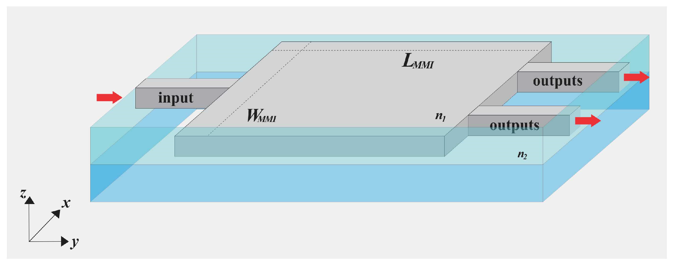
Figure 1. Multimode waveguide (1 × 2).
Nanomanufacturing 06 00003 g001
Figure 2. Normalized amplitude lateral field profiles.
Nanomanufacturing 06 00003 g002
Figure 3. Multilayer perceptron artificial neural network and transfer functions.
Nanomanufacturing 06 00003 g003
Figure 4. Artificial Neural Network Architecture.
Nanomanufacturing 06 00003 g004
Figure 5. Beam Propagation Method Solution vs. Artificial Neural Network (1 × 2).
Nanomanufacturing 06 00003 g005
Figure 6. Field formed by the self-image and solid model of simulations with data obtained through ANN 01-Tan-Tan-Tan of MMI devices (1 × 2) for wavelengths of 1.55 µm: (A) 2.00 × 5.3276 µm; (B) 3.00 × 11.3518 µm; (C) 4.00 × 19.5989 µm; and (D) 5.00 × 29.9786 µm.
Nanomanufacturing 06 00003 g006
Figure 7. Coordinates of the x-axis and y-axis obtained by the Beam Propagation Method vs. values obtained by ANN 01-Tan-Tan-Tan.
Nanomanufacturing 06 00003 g007
Figure 8. Comparison of efficiency between MMI devices (1 × 2) with 2.20 µm WMMI Beam Propagation Method and predictions by the best-performing Artificial Neural Network, for the wavelength integrating the E, S, C, and L bands.
Nanomanufacturing 06 00003 g008
Figure 9. Beam Propagation Method Solution vs. Artificial Neural Network (1 × 3).
Nanomanufacturing 06 00003 g009
Figure 10. Field formed by the self-image and solid model of simulations with data obtained through ANN A-Tan-Tan-Tan of MMI devices (1 × 3) for wavelengths of 1.55 µm: (A) 3.00 × 7.545 µm; (B) 4.00 × 13.095 µm; (C) 5.00 × 20.067 µm; and (D) 6.00 × 28.579 µm.
Nanomanufacturing 06 00003 g010
Figure 11. Coordinates of the x-axis and y-axis obtained by the Beam Propagation Method vs. values obtained by ANN A-Tan-Tan-Tan.
Nanomanufacturing 06 00003 g011
Figure 12. Comparison of efficiency between MMI devices (1 × 3) with 3.08 µm WMMI simulated by the Beam Propagation Method and predicted by the best-performing ANN, for the wavelength integrating the E, S, C, and L bands.
Nanomanufacturing 06 00003 g012
Figure 13. Field formed by the self-image and solid model of simulations with data obtained through ANN A-Tan-Tan-Tan of MMI devices (1 × 4) for wavelengths of 1.55 µm: (A) 4.00 × 9.93 µm; (B) 5.00 × 15.06 µm; (C) 6.00 × 21.41 µm; and (D) 7.00 × 28.97 µm.
Nanomanufacturing 06 00003 g013
Table 1. Historical evolution of multimode interference nanodevices.
YearInput × OutputLoss (dB)DimensionsMaterialsWavelength (nm)Reference
19941 × 160.8 dB (excess loss)W: 84; L: 1144Si, Al2O3 and SiO21000–2000[34]
19951 × N0.5 dB (insertion losses)W: 12–48; L: 200–3800GaAs and InP-based1550[19]
19961 × 4~0.3 dB (excess loss)W: 12; L: 340filters in InP/GaAs1500–1590[35]
19971 × 24.8 dB (excess loss)W: 40; L: 1000Erbium-doped film980[36]
19984 × 4~0.5 dB (excess loss)L: 1300Plasma-enhanced 1520–1580[37]
19991 × 2<0.5 dB (excess loss)W: 7.3; L: 435.5SiO2 and SiON1300 and 1550[38]
20001 × 4~2.23 dB (excess loss)W: 800; L: 10000Silver ion-exchange glass1530–1560[39]
20011 × 29.9 dB (excess loss)W: 4.6; L: 398SOI and SiO21550[40]
20023 × 40.95 dB (insertion losses)W: 125; L: 6332K+/Na+ soda-lime glass1550[41]
20031 × 21.5 dB (excess loss)W: 15; L: 500InP–InGaAsP1500–1600[42]
20041 × 81 dB (excess loss)W: 200; L: 11480Confined SOI1550[43]
20051 × 30.4 dB (excess loss)W: 23; L: 250Polymer850[44]
20061 × 22.75 dB (insertion losses)W: 50; L: 1321BenzoCyclobutene 1550[45]
20071 × 40.034 dB (excess loss)W: 28; L: 477AlGaAs-doped1550[46]
20082 × 20.6 to 2.3 dB (excess loss)W: 5.3; L: 34.18Air-cladded polymer1480–1630[47]
20091 × 23.9 dB (excess loss)W: 3; L: 18.1SOI1550[48]
20101 × 24.28 dB (insertion losses)W: 200; L: 220.36Io-exchange Ag+-Na+1550[49]
20111 × 223 dB (insertion losses)W: 200; L: 6552SOI1550[50]
20121 × 21.5 dB (insertion losses)W: 5.3; L: 6.5SOI1550[51]
20131 × 20.28 dB (excess loss)W: 1.51; L: 1.46SiO2 buried GaInAsP1548–1552[52]
20141 × 20.5 dB (insertion losses)W: 1.8 to 2.8; L: 1.5SOI1520–1580[53]
20151 × 20.4–0.8 dB (insertion losses)W: 3; L: 10.5SOI1540–1580[54]
20161 × 40.07 dB (insertion losses)W: 5; L: 12.3Polymer-based1530–1565[55]
20171 × 50.5 dB (excess loss)W: 25; L: 323.2Si3N4 and SiO2637, 647 and 657[56]
20181 × 80.11 dB (insertion loss)W: 4; L: 9.3GaN and SiO2500–600[57]
20191 × 20.46 dB (insertion losses)2.6 × 2.6 µm2Silicon and silica1550[58]
20201 × 2<0.21 dB (excess loss)W: 2.6; L: 6.6Silicon on insulator1550[59]
20211 × 40.62 dB (insertion losses)W: 11; L 36Silicon1550[60]
20221 × 20.6 dB (insertion losses)W: 2.5; L: 3.2Silicon-based1550[61]
20231 × 40.13 dB (insertion losses)W: 8.1; L: 39.6Silicon nitride (Si3N4)1260–1360[62]
20241 × 20.01 dB (insertion losses)W: 2.6; L: 34.4Lithium niobate1625–1675[63]
20251 × 30.47 dB (excess loss)W: 2.7; L: 6SOI 1500–1600[64]
Table 2. Parameter intervals.
ParametersIntervals
Wavelength (λ)1350–1600 nm
MMI width (WMMI)2.0–7.0 µm
MMI length (LMMI)5–30 µm
Core refractive index (Si)3.476
Substrate refractive index (SiO2)1.444
Output losses0.34–0.68 dB
Table 3. Hyperparameters.
HyperparametersValue
Network architecture
(1 × 2, 1 × 3, and 1 × 4 devices)
Three hidden layers, with [ten, eight, and five] and [five, eight, and ten] neurons respectively.
Activation functionsTansig (hyperbolic tangent) in hidden layers and Purelin (linear) in the output layer.
Loss functionMean Squared Error (MSE).
Optimizer (training algorithm)The Levenberg-Marquardt optimizer, for feedforward networks, offers fast convergence and numerical stability for nonlinear regression.
Learning rateA value of 0.01, automatically adjusted by the trainlm algorithm during training.
Number of epochsA value of 1000, as determined after convergence analysis.
Stopping criteriaMinimum MSE or gradient below 10−7.
Data splitOverall, 70% for training, 15% for validation, and 15% for testing.
Data normalizationLinear scaling to the range [−1, 1], compatible with the Tansig activation function.
Table 4. Global setting parameters.
ParametersValue
Core Refractive Index3.476
Substrate Refractive Index1.444
Index Difference2.032
Effective Refractive Index2.848
Wavelength in Free Space (µm)1.550
Waveguide Thickness (µm)0.220
PolarizationTE
Table 5. Performance of the three best Artificial Neural Networks using the Mean Squared Error of Cross-Validation as an evaluation criterion for the 1 × 2 device.
Hidden Layer Architecture
(Activation Function)
Number of
Neurons per
Hidden Layer
MSE Cross
Validation
RegressionTime (s)
ANN 01-Tan-Tan-Tan[ten, eight, and five]6.39410 × 10−50.9999977.46
ANN 02-Tan-Tan-Tan[five, eight, and ten]7.02583 × 10−50.99999714.40
ANN 03-Tan-Tan-Log[ten, eight, and five]7.57674 × 10−50.9999987.17
Table 6. Optical and geometric parameters of four MMI devices (1 × 2) obtained through the best-performing Artificial Neural Network with nomenclature ANN 01-Tan-Tan-Tan vs. Beam Propagation Method.
Optical and Geometric ParametersFigure 6AFigure 6BFigure 6CFigure 6D
BPMANNBPMANNBPMANNBPMANN
Wavelength (λ)1.5501.5501.5501.5501.5501.5501.5501.550
Substrate Refractive Index (n2)1.4441.4441.4441.4441.4441.4441.4441.444
Core Refractive Index (n1)3.47773.47773.47773.47773.47773.47773.47773.4777
Width—WMMI (µm)2.002.003.003.004.004.005.005.00
y-axis coordinate—LMMI (µm)5.3305.32711.35011.35119.60019.59830.03029.978
x1-axis coordinate (µm)−0.542−0.544−0.800−0.796−1.052−1.049−1.302−1.292
x2-axis coordinate (µm)0.5420.54440.8000.7961.0521.0491.3021.292
Losses (dB)0.380.420.510.550.600.630.670.68
Table 7. Performance of the three best Artificial Neural Networks using the Mean Squared Error of Cross-Validation as an evaluation criterion for the 1 × 3 device.
Hidden Layer Architecture
(Activation Function)
Number of
Neurons
per Hidden
Layer
MSE
Cross
Validation
RegressionTime (s)
ANN A-Tan-Tan-Tan[ten, fifteen, and twenty]1.7932 × 10−60.99999837.03
ANN B-Log-Log-Log[ten, fifteen, and twenty]4.0136 × 10−60.99999687.93
ANN C-Tan-Log-Pos[ten, fifteen, and twenty]4.2742 × 10−60.99999526.34
Table 8. Optical and geometric parameters of four MMI devices (1 × 3) obtained through the best-performing Artificial Neural Network with nomenclature ANN 01-Tan-Tan-Tan vs. the Beam Propagation Method.
Optical and Geometric ParametersFigure 10AFigure 10BFigure 10CFigure 10D
BPMANNBPMANNBPMANNBPMANN
Wavelength (λ)1.5501.5501.5501.5501.5501.5501.5501.550
Substrate Refractive Index (n2)1.4441.4441.4441.4441.4441.4441.4441.444
Core Refractive Index (n1)3.47773.47773.47773.47773.47773.47773.47773.4777
Width—WMMI (µm)3.003.004.004.005.005.006.006.00
y-axis coordinate—LMMI (µm)7.5507.54513.10013.09520.05020.06728.58028.579
x1-axis coordinate (µm)−1.056−1.054−1.393−1.392−1.712−1.716−2.061−2.059
x2-axis coordinate (µm)01.409.604.502.0
x3-axis coordinate (µm)1.0561.0541.3931.3921.7121.7162.0612.059
Losses (dB)0.340.370.450.550.480.480.580.58
Table 9. Activation function comparison.
Activation FunctionAdvantagesDisadvantagesPerformance
TansigHigh non-linear expressivityIt can saturateBest result (ANN 01)
LogsigIdeal for normalized dataHigher computational costGood, but less efficient (ANN 02)
PoslinSimple, fast, avoids saturationLinear trendLowest performance (ANN 03)
Table 10. Fabrication Tolerance Estimate for 10 nm Variation Intervals.
Parameter
Varied
Variation (∆)DeviceAffected Output
Parameter
Average Variation in Output
Parameter
Variation
(%)
Width (WMMI)±0.01 µm1 × 2 (W = 2.00 µm)Length (LMMI)±0.0266 µm±0.50
±0.01 µm1 × 2 (W = 5.00 µm)Length (LMMI)±0.0600 µm±0.20
Length (LMMI)±0.01 µm1 × 2 (L = 5.33 µm)Insertion Loss (IL)±0.01 dB±2.63
±0.01 µm1 × 2 (L = 30.03 µm)Insertion Loss (IL)±0.003 dB±0.45
Width (WMMI)±0.01 µm1 × 3 (W = 3.00 µm)Length (LMMI)±0.032 µm±0.42
±0.01 µm1 × 3 (W = 6.00 µm)Length (LMMI)±0.085 µm±0.30
Length (LMMI)±0.01 µm1 × 3 (L = 7.55 µm)Insertion Loss (IL)±0.015 dB±4.41
±0.01 µm1 × 3 (L = 28.58 µm)Insertion Loss (IL)±0.002 dB±0.34
Table 11. Comparison of results between work and this study.
MethodFontDeviceInsertion Loss (dB) 1550 nmComputational Cost/
Comments
PSO (Particle Swarm Optimization)[70]1 × 40.2–0.7 dBCost: hundreds to thousands of FDTD simulations during optimization; experimentally reported optimization time ranging from hours to days.
PSO/MMI applications[71]1 × N0.76–1.08 dBCost: high FDTD/BPM simulation load; improved implementations reduce costs, but they are still high.
Adjoint/topology optimization[72]1 × 2/1 × 4Can achieve very low losses—excellent performance at the physical limit.Cost: very efficient at parameter scaling (gradient calculation requires two simulations per iteration), but demanding implementation; results depend on regularization and constraints.
GA + DNN (hybrid)[73]Metasurfaces/
photonic
devices
Competitive performance, loss, and package depend on the case.Cost: GA requires multiple generations; DNN accelerates evaluation; hybrids reduce total cost compared to pure GA.
ANNThis work1 × 20.38 dB (ANN)
0.42 dB (BPM)
07.46 s
ANNThis work1 × 30.37 dB (ANN)
0.34 dB (BPM)
37.06 s
Disclaimer/Publisher’s Note: The statements, opinions and data contained in all publications are solely those of the individual author(s) and contributor(s) and not of MDPI and/or the editor(s). MDPI and/or the editor(s) disclaim responsibility for any injury to people or property resulting from any ideas, methods, instructions or products referred to in the content.