Article

Nano-Thin Oxide Layers Formed on Hydrogen Plasma Modified Crystalline Si for Advanced Applications

by
Sashka Alexandrova
1,2,*,
Anna Szekeres
2,* and
Evgenia Valcheva
3,4
1
Department of Applied Physics, Technical University Sofia, 8 Kl. Ohridski Blvd., 1000 Sofia, Bulgaria
2
Institute of Solid State Physics, Bulgarian Academy of Sciences, 72 Tzarigradsko Chaussee Blvd., 1784 Sofia, Bulgaria
3
Faculty of Physics, Sofia University “St. Kliment Ohridski”, 5 J. Bourchier Blvd., 1164 Sofia, Bulgaria
4
National Centre of Excellence Mechatronics and Clean Technologies, Sofia University “St. Kliment Ohridski”, 5 J. Bourchier Blvd., 1164 Sofia, Bulgaria
*
Authors to whom correspondence should be addressed.
Nanomanufacturing 2025, 5(3), 12; https://doi.org/10.3390/nanomanufacturing5030012
Submission received: 28 June 2025 / Revised: 21 July 2025 / Accepted: 6 August 2025 / Published: 12 August 2025

Abstract

Since the early days of silicon manufacturing, hydrogen gas treatment has been used to control the defect concentrations. Its beneficial effect can be enhanced using hydrogen plasma as a source of active atomic hydrogen. Hydrogen plasma modification of c-Si surface can be challenging because the plasma can induce precursors of defect centers that can persist at the interface and/or grown oxide after subsequent thermal oxidation. In the present study, we investigate nanoscale silicon dioxides with thicknesses in the range of 6–22 nm grown at low temperature (850 °C) in dry oxygen on radio frequency (RF) hydrogen plasma-treated silicon surface. The properties of these oxides are compared to oxides grown following standard Radio Corporation of America (RCA) Si technology. Electroreflectance measurements reveal better interface quality with enhanced electron mobility and lowered oxidation-induced stress levels when the oxides are grown on H-plasma modified c-Si substrates. These results are in good accordance with the reduced defect concentration established from the analysis of the current–voltage (I-V) and multifrequency capacitance–voltage (C-V) characteristics of metal-oxide-semiconductor (MOS) capacitors incorporating the Si-SiO2 structures. The study proves the potential of hydrogen plasma treatment of Si prior to oxidation for various Si-based applications.

1. Introduction

The rise and advance of the microelectronic industry since the 1970s was based mainly on Si technology. The key actor was the simple Si/SiO2 structure characterized by low interface state density and low leakage currents. The main road of development was a steady decrease in the transistor size to achieve faster and reliable functioning. The oxide nanometer thickness approaching tunnel limits caused the replacement of SiO2 with other isolation layers with a higher dielectric constant (high-k dielectrics) [1,2,3]. The most successful were mostly oxides, such as, e.g., HfO2, which would ensure a relatively good interface to Si due to the formation of intermediate to very thin SiO2, although compromising the dielectric constant. Nevertheless, the problem with the defects in the interfacial region has never been solved. Si/SiO2 continues to attract the interest of investigators concerned with the interface composition and structure, since it can be incorporated in more complicated devices.
Silicon dioxide, as a complementary metal-oxide-semiconductor (CMOS)-compatible oxide, has potential for advanced applications in renewable energy technologies, such as photovoltaics and storage batteries, and as a resistance switching material. Although known from its early developments, SiO2 has provoked an interest as an interfacial oxide for silicon-based passivating contacts in the progression to the next generation of silicon solar cells [4]. The electrical characterization of dielectric passivation layers in solar cells in the course of thermal oxidation technology processing is an obvious necessity [5]. Another field for advanced application of SiO2 as a promising material is lithium-ion storage [6]. Silicon oxide has also been studied as probably one of the most suitable materials for use in resistance-switching technologies [7].
Theoretical investigations have shown that a stoichiometric SiO2 layer can be achieved after building just two monolayers [8,9]. It remains to be confirmed experimentally. Even after long years of research, this could be a difficult task since the incorporation of O atoms into the Si crystal lattice depends on different factors during oxide formation that could vary in detail under different laboratory conditions. Precise investigations should connect the defect formation as a result of incomplete oxidation (imperfect atom ordering) and the leakage currents through the oxide, the major challenge being the control of technological processes in the nanometer range.
Since the early days of silicon manufacturing, hydrogen gas treatment has been used to control the defect concentrations [10]. Its beneficial effect can be enhanced using hydrogen plasma as a source of active atomic hydrogen. Hydrogen plasma modification of the Si surface can be challenging because the plasma can induce precursors of defect centers that can persist at the interface and/or grown oxide after subsequent thermal oxidation [11,12,13,14,15].
Depending on a wide number of factors, such as gas pressure, substrate temperature, geometrical parameters of the chamber, and potential distributions and locations of the samples inside it, using hydrogen plasma for the processes on the sample surface can be complicated, and their discrimination can be a difficult task. Nevertheless, some important issues still can be considered as decisive. These are the chamber pressure, the substrate temperature, and exposure time duration. The other parameters can be kept constant for a series of experiments. The concept is to create surface defect centers and provide a source of active hydrogen atoms in the same space. Further, during oxidation, SiOx nanolayers with a more perfect interface to the Si substrate can be achieved at relatively lower temperatures (below 900 °C). Hence, the passivation role of the active hydrogen atoms should be considered in more detail.
A huge number of scientific papers devoted to the Si-SiO2 interface have been published in the last five decades, because of its crucial role as a key component of CMOS transistors and integrated circuits in modern electronics. Moreover, it continues to play a significant role being integrated into other devices such as sensors, solar cells, and piezoelectric actuators. The reason is that Si-SiO2 elements can be produced with extremely high electrical quality of both the film and interface with relatively simple techniques, such as thermal oxidation in an ambient atmosphere containing oxidizing species. Thin SiO2 on Si using thermal oxidation in a dry and wet atmosphere is regarded as a standard technique and is well-documented [6]. Other, different techniques were attempted in plasma or solution ambient. Recently, oxidation techniques have been compared with respect to the preparation of high-quality ultra-thin oxide layers on crystalline silicon [9]. However, the chemical and physical mechanisms responsible for such perfect structures represent a profound fundamental challenge [16]. The structure of the SiO2/Si interface still remains elusive, especially for oxides in the tunnel depth range.
The ability of oxide layers to present as high-quality insulators is described by their leakage, dielectric strength (or dielectric breakdown voltage), and electrically active defects at the interface with the Si.
The aim of the present study was to grow nanoscale silicon dioxides on a c-Si surface modified in RF hydrogen plasma and investigate their electrical activity. In accordance with our previous investigations [11,17], hydrogen gas pressure was kept constant while varying the substrate temperature during plasma exposure. The oxide growth temperature of 850 °C was chosen as relatively low but still appropriate for growth of quality oxides and high enough to serve in annealing eventual Si plasma-induced defects.
Electrically active defects were tracked, measuring I-V characteristics and frequency dispersion of C-V characteristics of the formed MOS capacitors. Their concentration is evident for forming a high-quality SiO2-Si structure with low leakage currents. Electroreflectance measurements revealed better interface regions and lowered oxidation-induced stress levels when the oxides were grown on H-plasma modified c-Si substrates. The results prove the potential of hydrogen plasma treatment of Si prior to oxidation to effectively tune the interfacial properties and the associated electrical performance for various advanced Si-based applications.

2. Materials and Methods

2.1. Sample Preparation

In the present studies single-crystal silicon (c-Si) Wacker wafers of n-Si(111) and p-Si(100) with (5–10) Ω cm and (4–10) Ω cm, respectively, served as substrates. Before any technological processes, all samples underwent a standard Radio Corporation of America (RCA) wet cleaning procedure [18]. The chemicals in the RCA cleaning were with 99.99% purity Merck’s “Suprapur” products.
After the RCA cleaning the substrates were divided in parts, keeping one of them for reference. The other substrates were put in a planar reactor and exposed to hydrogen plasma, excited by an RF generator working at 13.56 MHz and power density of 75 mW/cm2 delivered to the upper electrode. The substrates were placed on the lower electrode, which was set to ground together with the whole reactor’s metal body. The hydrogen gas pressure was 1 Torr (133 Pa) and the duration of the plasma exposure was 15 min. The substrates were either treated without heating (for the sake of brevity hereafter marked as 20 °C) or with the electrode plate heated up to a substrate temperature (Tsubst) of 100 °C or 300 °C.
The plasma-treated substrates were oxidized together in the same runs with the reference ones that were not exposed to hydrogen plasma. The oxidation process was performed in a conventional horizontal atmospheric furnace at 850 °C in dry oxygen, H2O content being less than 3 ppm. The oxidation times were varied to grow thin oxides with thicknesses in the nano range. After the oxidation was completed, oxygen was switched to nitrogen flow and the samples were removed in nitrogen at atmospheric pressure. The thickness of the grown oxides, estimated by ellipsometric measurements, varied in the range of 6–22 nm, depending on the pre-oxidation treatment, either RCA cleaning only or with subsequent hydrogen plasma treatment.
We want to highlight that no further thermal treatment was applied to the Si-SiO2 structure formed by the above technological processes.
In order to assess the electrical properties of the oxidized samples, MOS capacitors were formed by vacuum evaporation of Al dots. As a contact to the silicon backside, a continuous Al film was evaporated.

2.2. Characterization Methods

In order to characterize the obtained SiO2 layer and the Si-SiO2 interface, capacitance–voltage (C-V) and current–voltage characteristics (I-V) measurements of the MOS capacitors were performed. The C-V measurements were taken in the frequency range of 1 kHz to 300 kHz and 30 mV test signal with a Precision Component Analyzer WAYNE KERR 6425 (Wayne Kerr, London, UK). The current–voltage dependences were recorded with Hewlett-Packard Model 4140A pA Meter (Hewlett-Packard, US) with integrated DC bias source. All measurements were performed at room temperature in light-shielded conditions.
Information about the concentrations of the electrically active defects in the MOS capacitors was obtained by analysis of the frequency dispersion of the capacitance–voltage curves. The densities of fixed oxide charge ( N f ) and the interface trap density ( N i t ) were evaluated by comparison of the experimental and ideal theoretical C-V characteristics.
The state of silicon surface in the formed SiO2-Si structures was characterized applying electromodulated reflectance (electroreflectance) measurements in the photon energy range of 3–3.7 eV, covering the range of the Si direct bandgap energy with its critical points. The measurements were carried out at room temperature using an electrolytic cell with 0.1 N KCl solution. As Si-backside contact thin indium layers were used. The voltage applied to the samples was in the low external field regime with modulating voltage value below 1 V. From the analysis of line shapes and the polarity of the electroreflectance (ER) spectra, the transition energy ( E g ), being the Si direct energy gap at the critical point of Brillouin zone at k = 0, and the phenomenological broadening parameter (Γ) were calculated using the Aspnes three-point technique [19].

3. Results

3.1. Electroreflectance Spectroscopy

Electroreflectance (ER) spectroscopy is sensitive to changes in the electronic structure of the material. The technique is particularly suitable method for examining the surface condition, as the beam of the reflected light tests the surface from the interface side in the Si/SiO2 structure, Si volume being of less importance. Analysis of the ER responses can help to trace any fine changes in the silicon surface regions caused during technological processes. Also, ER spectra provide information about the energy gaps at critical points of the Brillouin zone.
Typical ER responses from silicon surface layers with very thin SiO2 on p-Si(100) and n-Si(111) reference substrates are presented in Figure 1a. The difference in thicknesses comes from the different oxidation rates for the two crystal orientations of Si, as numerous studies have shown the oxide growth is faster for Si with (111) orientation [20,21]. For the p-Si(100) references the spectrum polarity is “+; −” while for the n-Si(111) it is “−; +”, which is a typical observation for p- and n-type Si, respectively [22].
Hydrogen plasma exposure of Si prior to oxidation changes considerably the line shapes of the ER spectra, as is evident from Figure 1b,c. Analyzing the line shapes around the direct energy gap of silicon shows the strong influence of hydrogen plasma, which can be registered even after oxidation at 850 °C.
In comparison to reference samples, pre-oxidation plasma treatment with hydrogen resulted in opposite ER signal polarities of “−; +” in p-Si samples. In n-Si(111) samples, this effect appears only when the substrate was kept at 100 °C during plasma exposure. This temperature is not high enough to anneal some radiation defects, which may compensate dopant charges. Such a reversal of the ER polarity can be observed when the electric field causes inversion of the surface [23]. In our case, the inversion of the surface field could appear due to process-generated defects in the thin Si subsurface layer, but their concentration cannot be high, considering the well-defined ER spectra [19]. Hydrogens from the plasma, entering the Si substrate, can react with defect states (like H+ + Si-H = H2 + Si+), creating Si+ dangling bonds, the most significant interface defects [24,25]. Due to the formed inversion layer, these defect states will capture electrons and will be charged negatively [25], causing inversion in the surface electric field and thus changing of the sign of the ER spectra. Our earlier studies of nanoscale oxides grown in low-energy H+ implanted c-Si(100) have also registered the polarity reversal of the ER signal [12]. The beneficial effect of the presence of hydrogen species in the interfacial region was attributed to the creation of favorable conditions for oxide growth in a less dense and strained Si structure [12].
Applying the Aspnes three-point method [15], the line shapes in the ER spectra were analyzed and the direct energy gap ( E g ) and the energy broadening parameter (Γ) values were determined and are summarized in Table 1.
The direct transition energies E g are slightly shifted to lower energies relative to an unstressed bulk Si, for which this direct transition energy gap ( E g d ) is known to be 3.4 eV [26]. Any shift of the E g value relative to that of the unstressed silicon is an indication for the internal stress ( σ S i ) generated by the pre-oxidation procedures and subsequent oxidation. This stress level can be determined from the relationship σ S i = k × E g d E g , where k is the correlation coefficient, equal to 2.09 × 10¹⁰ Nm−2eV−1 [27]. The results are summarized in Table 1.
The stress in Si has been found to be tensile while the grown oxide layer is under high compressive stress. Higher values of order of l09 Nm−2 are typical for dry oxides grown at 850 °C and above [27,28]. In our oxides grown in the given technological conditions, the tensile stress in Si has considerably low values (Table 1) and, therefore, the corresponding compressive stress generated in the oxides will also be lower than that usually observed for Si oxidation at 850 °C. Compared to the data of RCA references, hydrogen plasma treatment reduced the σ S i levels even more. Although the oxidation-induced stress has a common origin arising from the volume expansion in silicon, the tensile stress level is slightly higher for p-Si(100), as has already been established [28].
Energy broadening parameter is a characteristic for defect concentrations in the Si surface region and, hence, an indication for surface perfection. Reduction in the Γ values for oxides grown on plasma-modified Si (Table 1) is evidence for improved Si-SiO2 interface quality. For p-Si(100), the hydrogen plasma treatment leads to a reduction in the energy broadening and the tensile stress levels compared to the reference sample. However, despite the lower stress levels in the n-Si(111), Γ values are larger compared to p-Si(100) series, pointing to higher concentrations of interface defects. This is particularly pronounced for the hydrogen plasma-modified Si(111) without heating (Tsubst = 20 °C) (Figure 1c and Table 1). Also, the Γ parameter is proportional to the carrier relaxation time (τ) (Γ~ 1/τ) [29] and, therefore, the mobility of free carriers near the interface region can be estimated. The decrease in Γ value can be connected to lower scattering and increased charge carrier mobility, which plays an important role in device performance. In Table 1, the mobility values of hydrogen plasma-treated silicon are presented, normalized to the values of the reference samples.
The ER results point out that oxidation of hydrogen plasma-modified Si substrates as a whole resulted in an improvement of the interface, reflected in lower internal stress levels, in smaller amount of defects and higher mobility of free carriers. However, hydrogen plasma exposure has different effects on the properties of the Si(100) and Si(111) interfaces (Table 1), as for n-Si(111) these beneficial effects are less pronounced. It could be concluded that better results are obtained for oxides grown on plasma-treated n-Si or p-Si heated at Tsubst = 100 °C. However, the change in the polarity for plasma-modified p-Si(100) points to persistent defects that compensate the doping density. For n-Si(111) this effect can be seen only for plasma exposure at Tsubst = 100 °C. For that reason, the results of plasma technological conditions over references can be stated as best for substrate temperature of 300 °C. These observations are in good agreement with the results of the electrical studies presented and discussed in the next sections.
Based on the above observations, further herein we will concentrate on comparing the electrical properties of MOS structures which were formed with oxides grown on Si substrates either without heating (20 °C) or heated to 300 °C during plasma exposure, with those MOS structures formed on Si substrates undergoing only RCA cleaning.

3.2. Electrical Properties

In this section we will consider in more detail the I-V characteristics and the frequency dispersion behavior of the C-V characteristics, aiming to reveal the mechanism of charge carrier transport through SiO2-Si structures and to obtain information about the state of the formed Si-SiO2 structures brought by the proposed technological processes.

3.2.1. Charge Carrier Transport Through SiO2-Si Structure

Let us briefly introduce the conduction mechanisms for most often regarded physical phenomena in the semiconductor/oxide structure, namely Schottky emission (SE), Poole–Frenkel (P-F) emission and Fowler–Nordheim (F-N) tunneling [10] or trap-assisted tunneling (TAT) [30]. The expressions for the current carried out through a MOS structure by the above-mentioned carrier transport mechanisms are presented in Table 2.
The Schottky emission (SE) is an electrode-limited conduction mechanism in which the electrons can gain enough energy through thermal excitation and can be injected over the energy barrier at the interface into the dielectric. The lowering of the potential barrier by the image force is known as the Schottky effect. The linearized plot of the logarithmic J versus V1/2 dependence gives an indication that this process dominates the conductance. In the case of Poole–Frenkel (P-F) emission, the conduction mechanism is bulk-limited, involving field-assisted excitation and emission of electrons from traps into the conduction band of the dielectric. Establishing a linear plot of ln(J/V) versus V1/2 would indicate that such a mechanism is involved. Fowler–Nordheim (F-N) tunneling is a quantum mechanical effect. Electrons tunnel through a short path of the triangular part of the barrier at the electrode, which is possible due to the field-induced barrier lowering. This conduction mechanism can be characterized by a ln(J/V2) versus 1/V plot. Trap-assisted tunnelling is less likely to occur due to the small oxide thickness, and thus, it is not considered here.
In the equations, E is the electric field on the insulator, φ B is the energy barrier at the injecting interface, φ T is the energy depth of the traps, μ is the electronic mobility in the dielectric, and N C is the effective density of states in the conduction band. The constants include the electronic charge (q), vacuum permittivity ( ε 0 ), optical dielectric constant ( ε o x ), free electron mass ( m o ), effective electron mass in the oxide layer ( m * ), absolute temperature (T), Boltzmann’s constant ( k B ) and the Plank’s constant (h).
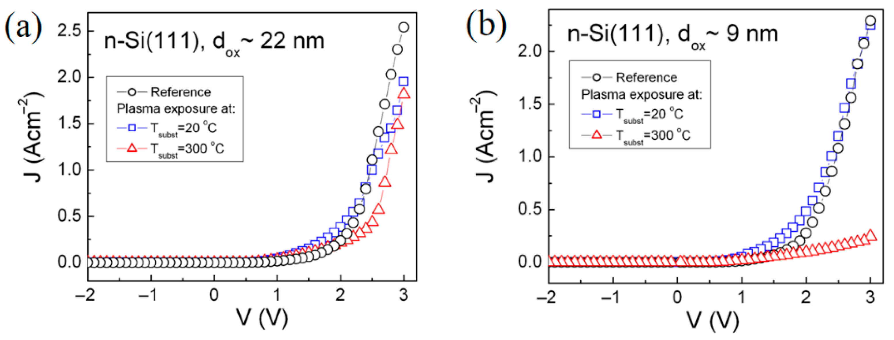
The current density (J) (current per unit area) versus voltage, (J-V) characteristics of MOS capacitors with oxides grown on n-Si(111) substrates with different pre-oxidation history and different oxide thicknesses are comparatively shown in Figure 2. The J-V dependences for oxides grown on p-Si(100) are similar qualitatively and in trend to those for n-Si(111) but the currents are significantly smaller even at higher fields, as will be also shown further.
From Figure 2, low reverse leakage currents are evident. From this point of view, we will consider only the forward J-V characteristics for both kinds of substrates in the voltage range from 0 to 3 V, where the electrical field is still relatively low so that no breakdown events are to be expected. Two voltage regions can be discriminated, which should be discussed related to different mechanisms of charge carrier transport as follows.
Small voltages (low electric fields) correspond to low leakage conditions (Figure 2). As the electric field increases, the curves exhibit a slow rise in leakage current followed by a sharp increase but without evidence of breakdown phenomenon. For the thinner oxides, the sharp rise started at a higher electric field. No breakdown events were noticed up to 1.5 × 10⁶ Vcm−1 for 22 nm oxides and up to 3 × 10⁶ Vcm−1 for 9 nm oxides. These observations indicate that structural defects from plasma exposure have relatively small concentrations, as was supposed from the ER spectra analysis above. Any difference in the conduction mechanisms should be attributed to the hydrogen atoms incorporated during plasma exposure.
In accordance with the carrier transport mechanisms outlined above, we analyzed the measured J-V characteristics using the equations in Table 2. The identification of the dominant mechanism would lead to the conclusion whether the current is controlled through contact (barrier) injection or bulk (traps) mechanism, which can have implications on the oxide structure.
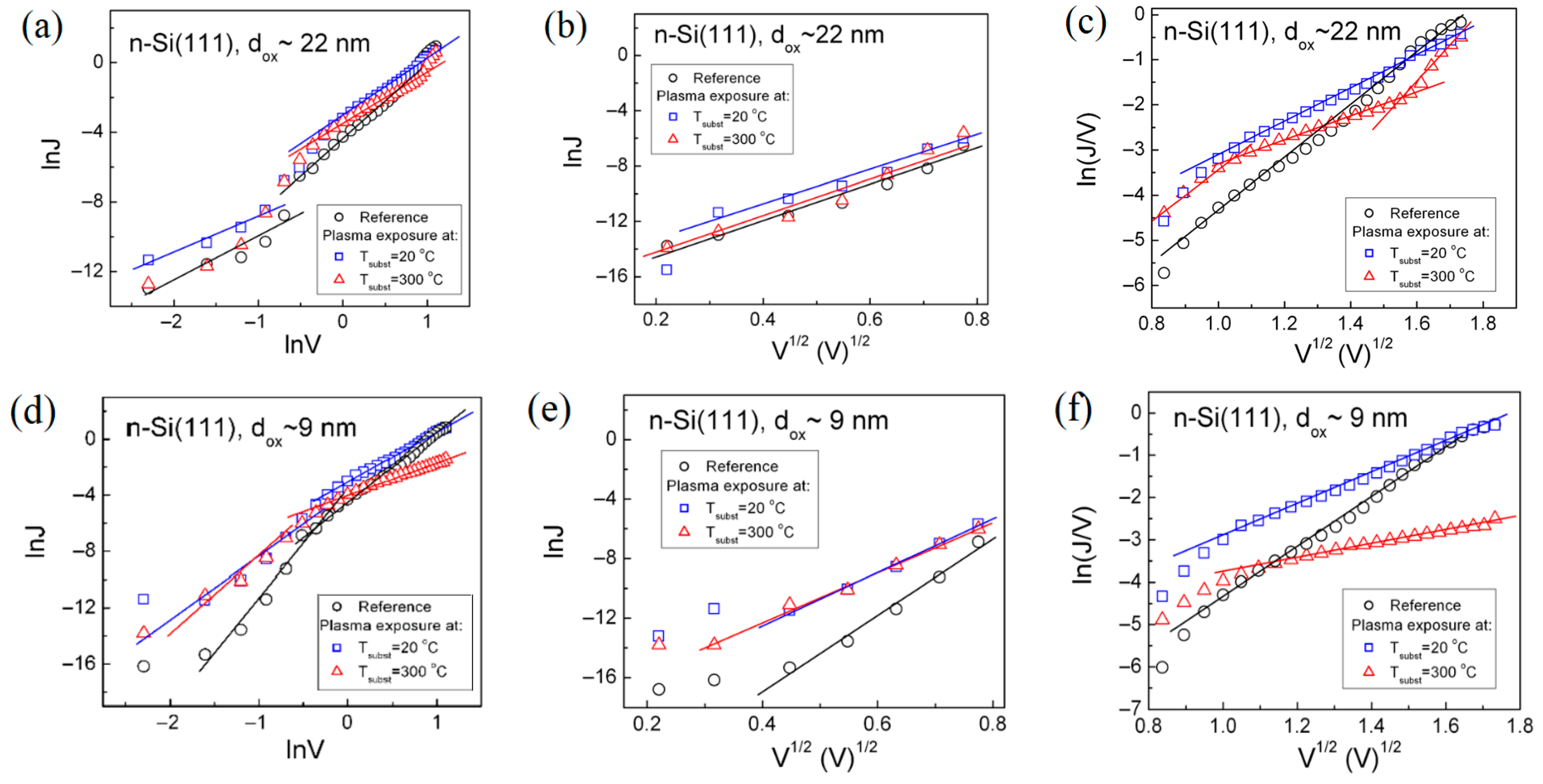
In order to analyze the conduction mechanisms, plots are constructed fitting the experimental data in Figure 2 with corresponding expressions given in Table 2. These plots are presented in Figure 3 and Figure 4 for n-Si(111) and p-Si(100) substrates, respectively.
Usually, linear plots are generated according to the equations given in Table 2 to draw conclusions about the conduction mechanisms. However, depending on the applied voltage, linear sections with different slopes were identified in the plots in Figure 3 and Figure 4 so that discrimination may not be trivial. Conclusions were based mainly on the accuracy of the linear regressions.
In Figure 3, results are given for oxides on n-Si(111) with thickness of ~22 nm and ~9 nm. In Figure 3a,d, the two voltage regions mentioned above can be better resolved from the lnJ versus lnV plots, but no relevant mechanism can be inferred. A better insight for the conduction processes can be taken from Figure 3b,c,e,f, where the J-V plots are presented considering models typically applicable for thermally grown oxides [30].
The linear relationship of the lnJ versus V1/2 plot in Figure 3b,e suggests that the Schottky emission mechanism can be regarded as dominating in the low leakage range of electric fields over the oxide up to about 2.5 × 10⁵ Vcm−1 (0.5 V) and 1.1 × 10⁶ Vcm−1 (1 V) for both ~22 nm and ~9 nm oxides, respectively. For higher electric fields the Poole–Frenkel trap emission modeling fits better to the data (Figure 3c,f). Most probably, during plasma exposure pre-oxidation defects were created that persist even after the oxidation, as suggested above from the ER study. In both voltage regions the exact parameters of the linear regressions depend on the pre-oxidation treatments of the Si substrates, namely, with reference (RCA clean only) or with hydrogen plasma treatment at different substrate temperatures. Analysis of the J-V curves by the Fowler–Nordheim tunneling model could not give a reasonable result. In this case F-N tunneling cannot be considered as an active process.
The results presented in Figure 3 are discussed in the same terms for both oxide thicknesses with the dominant conduction mechanisms being SE in the low-voltage region, followed by P-F trap emission for higher voltages. Such conclusions seem reasonable based on the qualities of the fits. Up to a certain electric field, where the slopes change (at about 2.5 × 10⁵ Vcm−1 and 1.1 × 10⁶ Vcm−1 for ~22 nm and ~9 nm oxides, respectively), the lowering of the injection barrier sustains the leakage current, indicating Schottky emission current mechanism. P-F emission begins at higher electric fields needed in order to start the de-trapping process. There is a region of mixed SE and P-F carrier conduction for voltages between 0.8 and 1 V.
A similar approach was applied to the oxides grown on p-Si(100) under the same conditions and the same runs as for the n-Si(111) considered above. It should be mentioned that the oxide thicknesses are smaller on Si(100) than that on Si(111) because of the slower oxidation rate of (100) oriented crystalline Si [20]. This effect is also observed in our experiments on growing oxides on hydrogen plasma-treated substrates [32]. Exemplary selected results are shown in Figure 4 for oxides with ~12 nm and ~6 nm thicknesses on Si(100) substrates treated in plasma at 20 °C and 300 °C prior oxidation. For both thicknesses, application of SE and P-F emission plots leads to similar conclusions for two conduction mechanisms, controlling the leakage at low and higher electric fields, respectively.
A common feature of the lnJ versus lnV plots constructed from all measured J-V characteristics presented above (Figure 3a,d and Figure 4a,b) is the change of the slope with increasing voltage. This is an indication of different carrier transport mechanisms through the oxide for different voltage ranges. Further analysis showed that in the low voltage range of 0 to 0.8 V, the J-V curves could be best fitted by the equation describing the SE model, indicating an electrode-limited mechanism (Figure 3b,e and Figure 4c).
In the case of oxides grown on n-Si(111), the carrier injection is from the Si-SiO2 interface, while for oxides grown on p-Si(100), injection is related to the Al-SiO2 interface. The main differences for the oxides on n-Si or p-Si material would be related to the different barriers at the injecting interfaces.
The slopes of the fitting lines in Figure 3b for ~22 on n-Si(111) nm oxides show close values regardless of substrate temperature during plasma exposure. The same behavior can be traced for ~9 nm thin oxides, as seen in Figure 3e, but the slope for the reference oxide exhibits dependence on oxide thickness. Since the results represent Schottky emission from the Si-SiO2 interface, pre-oxidation plasma exposure may be the cause of the change in the barrier heights in comparison of the reference oxides.
For p-Si(100) samples, the slopes in Figure 4c have similar values independent of pre-oxidation procedures. This is reasonable, since in this case, the injection comes from the Al-Si interface, which is not related to plasma influence.
In the high voltage range, above 0.8 V, the best fit can be achieved by considering the Poole–Frenkel conduction mechanism.
In Figure 3c,f as well as in Figure 4d, different slopes of the linear regressions are observed depending on the pre-oxidation conditions and the thickness of the oxides. This should be an indication of the presence of oxide traps in the gap of the oxide with different energy levels. In the reference oxides, regardless of the type of doping, n-Si or p-Si, only one trap can be seen. For all other oxides more than one trap level can be inferred. This means that the defects generated during plasma exposure persist after oxidation with different atomic surroundings in the SiO2 lattice with the probable involvement of hydrogen in these processes [12,13,33].
As a whole, a scrutinized insight in the J-V characteristics of the MOS capacitors with oxides grown with the above-described pre-oxidation treatments can lead to the following implications. For all oxides on plasma-modified Si substrates, lower leakage currents are observed compared to the references, with the lowest levels observed for plasma treatment at Tsubst = 300 °C. No indications of breakdown are seen in both reverse and forward directions up to 5 MVcm−1. For all oxides, the presence of traps in the oxide was evident and this issue is discussed further, analyzing the C-V characteristics of the formed MOS capacitors.

3.2.2. Frequency Dispersion Behavior of the C-V Dependences of the SiO2-Si Structure

According to the experimental results in Section 3.2.1, hydrogen plasma treatment prior to oxidation improves the interface quality and electrical characteristics compared to conventional thermal oxidation procedures. However, charge can be stored in the oxides in residual traps from plasma exposure and can affect the parameters of a MOS capacitor, the main building cell of the MOSFETs.
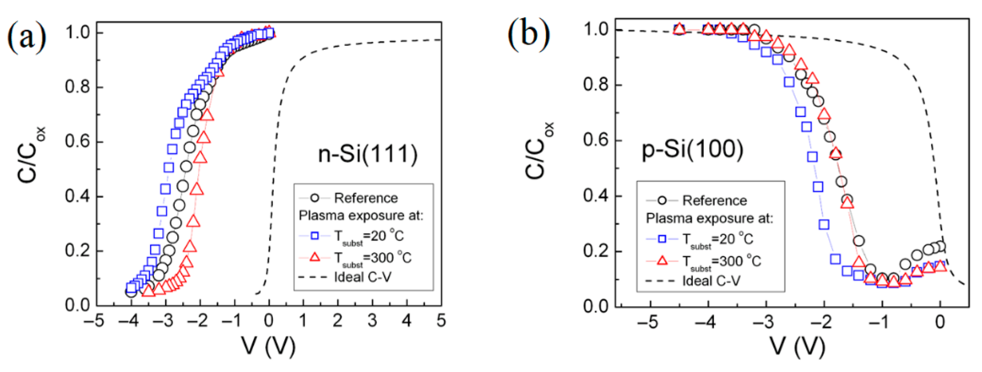
It is well known that information about the densities of the oxide charge and traps located sharply at the interface can be inferred from C-V measurements. Oxide charges, fast and slow interface states, can be distinguished. In Figure 5 the C-V curves of MOS capacitors with oxides on n-Si and p-Si are presented. Also, the corresponding so called “ideal” C-V curve, theoretically calculated for the case when no charges are present, is included. Estimation of the oxide charge was made by calculating the flatband capacitance C f b from the following equation [10]:
C f b C o x =   1 1 +   ε o x ε S i d o x ε 0 ε S i k T q 2 N A , D     ,
where C o x is the oxide capacitance in strong accumulation, ε 0 ,   ε o x   and ε S i are the dielectric constant of vacuum, oxide and silicon, respectively, N A , D is the concentration of dopants. The rest of the quantities have their known meaning.
As a reminder, the flatband condition in MOS capacitor referred to the condition when there is no electric field in the Si and the bands are flat. The applied voltage that brings this state is given by
  V f b = Φ m s Q f + Q i t / C o x     ,
where Φ m s is the work function difference between Si and the Al gate, and Q f and Q i t are the charges captured in the oxide and interface traps, respectively [10].
In Figure 5, an experienced eye can see the differences in C-V curves of plasma-treated Si substrates compared to those on standard RCA-treated Si. The shifts from the ideal curves indicate positive oxide charges ( Q f ), which are well known to build in the thermal oxide [10]. The highest Q f values appear for both n-Si and p-Si treated in plasma without heating, indicating the presence of generated oxide defects. This is in accordance with the results in the previous sections. Besides shifts, distortions of the C-V curves are also evident, pointing to charges trapped in residual interface traps generated during plasma exposure. Pronounced distortion, seen as a bump in the C-V curve, appears for oxides grown on n-Si(111) treated in plasma at 20 °C. The smallest shifts, i.e., the smallest Q f charges and slopes closely resembling the ideal C-V curve, are observed in MOS capacitors with oxides on Si exposed to plasma at Tsubst = 300 °C. The role of the hydrogen atoms migrating through the growing oxides may contribute to these beneficial results.
The highest Q f values are observed for both n-Si and p-Si treated in plasma without heating, indicating the generation of oxide defects. This is consistent with the results in the previous sections.
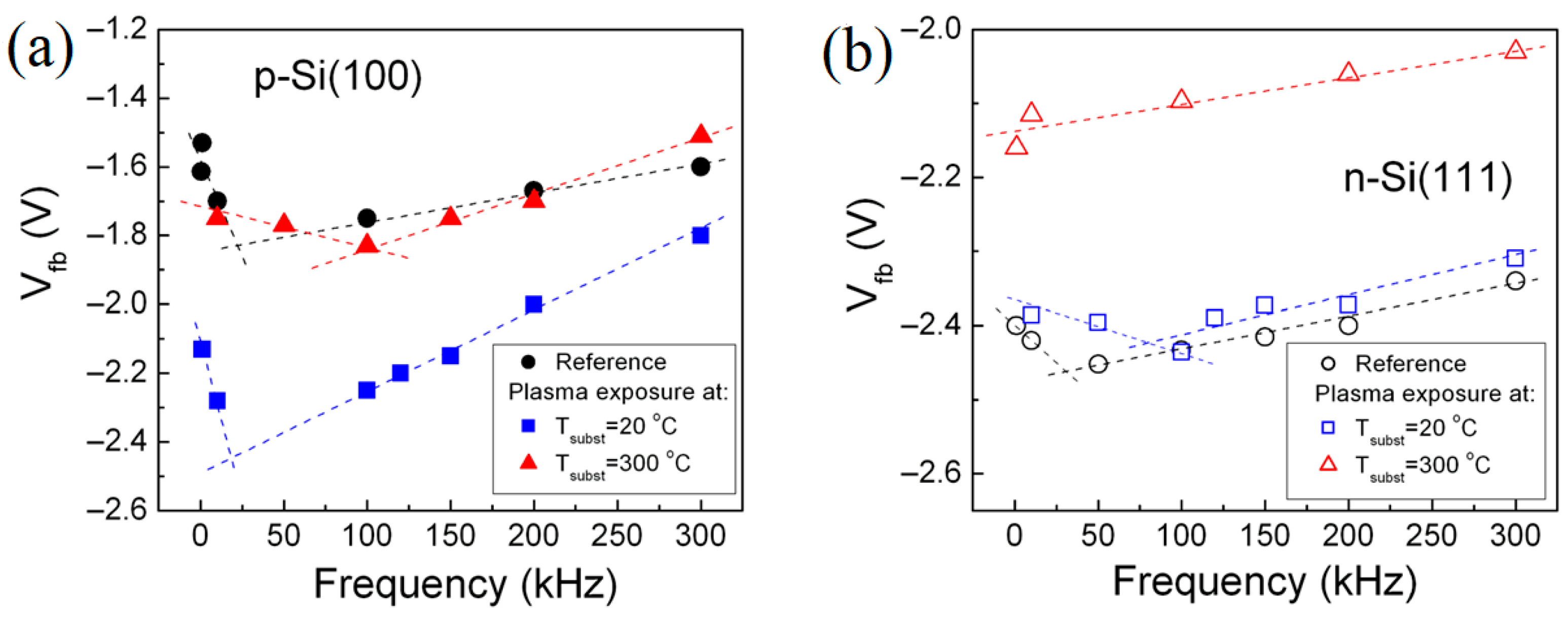
Further insight can be gained from the multifrequency measurements. The results are summarized in Figure 6, where the flatband voltage shifts with the AC frequency for MOS capacitors on p-Si(100) (Figure 6a) and n-Si(111) (Figure 6b) are presented. If the frequency is high enough, Q f can be estimated from the C-V shift. As the frequency decreases, interface traps start to react and make a contribution, increasing the voltage shifts. The interface traps in the upper half of the Si bandgap are considered as acceptor-type centers, contributing to the fixed positive charge Q f . With further decrease in the frequency, the V f b shifts come to a turning point, corresponding to flatband values V t at which V f b decreases up to the values corresponding to the lowest frequency. This can be a result of slow donor-type interface traps that start to contribute negative charges. Their density can be estimated from the V f b shifts at the lowest frequency. The turning point can be related to the fast interface traps Q i t , so an estimation of the amount of Q i t can be taken from the difference Q i t = Q f Q t .
The densities of the interface defects are summarized in Table 3. The values are in support of the observations discussed in Section 3.2.1 and Section 3.2.2.

4. Discussion

The role of hydrogen has a long story in semiconductor technology. Treatment in hydrogen-containing atmosphere, often forming gas, has been applied not only in silicon technology. The searched effect was annealing of structural defects mostly by saturating dangling bonds. Such treatments are applied at low temperatures up to about 450 °C or slightly lower.
The most important implication of our study is that the beneficial effect of hydrogen plasma applied as pre-oxidation treatment of Si on the Si-SiO2 interface properties is stable even after oxidation at 850 °C. Such a result cannot be ascribed to a simple saturation of the Si dangling bonds with hydrogen atoms. It should be related to a restructuring of the SiO2 lattice near the interface with Si.
Plasma treatment leaves the Si surface with a loose structure containing voids and distorted bonds. Our previous studies are in support of such an assumption [12,34,35]. Atomic force microscopic (AFM) imaging [33] showed that exposure of bare Si to hydrogen plasma did not cause appreciable surface roughening despite randomly distributed small hillocks, attributed to enhancement of oxidation rate at local surface defects. Nevertheless, the root mean square (rms) roughness values remained at an acceptable level below 0.2 nm [34], being a requirement for manufacturing high-quality MOS devices.
The exact condition of the Si surface after plasma modification depends on the substrate temperature during plasma exposure and the surface orientation as well. An important point is that hydrogen atoms migrate into the subsurface layer. Because of this, the pre-oxidation state of the hydrogen plasma-exposed Si surface layer is characterized by the presence of defect states and incorporated hydrogen atoms. This would stimulate the oxidation process, increasing the oxidation rates, which has already been reported in our previous studies [15].
From the presented results generation of defects is seen in oxides grown on hydrogen plasma-modified Si substrates without heating (20 °C) during plasma exposure. An improvement is observed for oxides grown on Si heated at 300 °C during plasma exposure, as the resulting Si-SiO2 parameters are better in comparison to the rest of the studied structures built on n-Si(111) and p-Si(100) substrates. Apparently, the combined effect of hydrogen incorporation and defect creation, together with the higher substrate temperature, in this case provides the best structural ordering of the Si-SiO2 interface and contributes to a higher perfection of the oxide random network. Atomic hydrogens from the plasma are active species in the process, contrary to molecular hydrogens in standard H2 annealing. It can be concluded that pre-oxidation treatment in hydrogen plasma can serve as a prerequisite for obtaining interfaces with enhanced quality. Similar results have been obtained when we have oxidized Si wafers after introducing hydrogen species in a shallow Si surface region by RF plasma immersion implantation of low-energy H+ ions [12,35]. From the results it has been concluded that hydrogen promotes structural ordering of the growing oxide and interface with the Si resulting in reduced internal stress and thinner interface region, which predicts better electrical characteristics of Si–SiO2 structures, as we observed here in the present study. Improvement of the Si-SiO2 structures was also observed elsewhere [14], where the atomic hydrogen was introduced through a technologically not-very-convenient technique injecting the hydrogen atoms from heated W wire.
The processes occurring in the proposed technological sequence can be summarized as follows. During plasma exposure defects are created and hydrogen atoms are incorporated in a thin subsurface layer. During subsequent oxidation at 850 °C, hydrogen atoms migrate through the growing amorphous oxide lattice, contributing to more complete oxidation. When discussing the nature of defects involved in the plasma, it should be remembered that there may be a variety of defect centers with different locations from the Si-SiO2 interface through the oxide, which have been extensively studied. Detailed information about their structural ordering and dependence on the technological conditions can be found in recent reviews [16,36].
The basic interface defects are Pb centers (•Si≡Si3) [24,37], oxygen vacancies [37] and Si dangling bonds with different surroundings [24,25]. The role of hydrogen during formation of Si-SiO2 interface is twofold. On one hand, hydrogen species penetrating into Si will passivate dangling bonds at the surface, in this way lowering the structural strains and reducing the interface defect concentration. On the other hand, they can dissociate and produce Si-H, Si-OH and other defects [38,39], leading to the opposite effect. Apparently, which one will prevail depends on the substrate temperature during plasma exposure and the amount of hydrogen species entering into the Si surface layer. Most probably, in our experiments it is not exactly passivation of defects with hydrogen that occurs. Otherwise, it would lead to outdiffusion of the hydrogen through the growing oxide and no interface improvement would be observed. Therefore, the process is rather a rearrangement of the oxide and interface structure in which hydrogen has a catalytic role.

5. Conclusions

Hydrogen plasma modification of c-Si surface applied as pre-oxidation treatment can serve as a prerequisite for obtaining Si-SiO2 interfaces with improved quality in comparison to standard microelectronic technology. From the electroreflectance spectroscopic study, it was found that the near Si surface region is in a low stress state with increased carrier mobility. Decreased densities of oxide and fast and slow interface defects were established from I-V and multifrequency C-V measurements. The effect was attributed to complicated interplay of defect generation, atomic hydrogen involvement and restructuring of the interface and oxide network.
New aspects regarding the Si-SiO2 system are constantly emerging, showing great potential for future development of advanced Si-based devices, where the Si-SiO2 structure is still the main constituent.

Author Contributions

Conceptualization, S.A. and A.S.; methodology, A.S. and S.A.; validation, S.A., A.S. and E.V.; formal analysis, S.A. and A.S.; investigation, S.A., A.S. and E.V.; data curation, S.A., A.S. and E.V.; writing—original draft preparation, A.S., S.A. and E.V.; writing—review and editing, S.A., A.S. and E.V.; visualization, A.S. and S.A.; supervision, A.S. and S.A.; project administration, A.S. and S.A. All authors have read and agreed to the published version of the manuscript.

Funding

This research received no external funding.

Data Availability Statement

The data presented in this study are available on request from the corresponding authors.

Acknowledgments

Evgenia Valcheva acknowledges the partial support by Project BG16RFPR002-1.014-0006 “National Centre of Excellence Mechatronics and Clean Technologies”, co-funded by the European Union, under “Research Innovation and Digitization for Smart Transformation” program 2021–2027.

Conflicts of Interest

The authors declare no conflicts of interest.

References

  1. Ramkumar, K. Charge trapping NVMs with metal oxides in the memory stack. In Metal Oxides for Non-Volatile Memory Materials, Technology and Applications; Dimitrakis, P., Valov, I., Tappertzhofen, S., Eds.; Elsevier: Amsterdam, The Netherlands, 2022. [Google Scholar] [CrossRef]
  2. Huang, A.P.; Yang, Z.C.; Chu, P.K. Hafnium-based High-k Gate Dielectrics. In Advances in Solid State Circuit Technologies; InTech: Houston, TX, USA, 2010. [Google Scholar] [CrossRef]
  3. Sharma, U.; Kumar, G.; Mishra, S.; Thomas, R. Advancement of Gate Oxides from SiO2 to High-k Dielectrics in Microprocessor and Memory. J. Phys. Conf. Ser. 2022, 2267, 012142. [Google Scholar] [CrossRef]
  4. Arul Prishya, A.S.; Chopra, L.; Manikanika. Comprehensive review on uses of silicon dioxide in solar cell. Mater. Today Proc. 2023, 72, 1471–1478. [Google Scholar] [CrossRef]
  5. Glunz, S.W.; Feldmann, F. SiO2 surface passivation layers–a key technology for silicon solar cells. Sol. Energy Mater. Sol. Cells 2018, 185, 260–269. [Google Scholar] [CrossRef]
  6. Ferdous, A.R.; Shah, S.S.; Hussain, A.; Mirghni, A.A.; Hardianto, Y.P.; Aziz, M.A. Review on current advancements in silica and their composites for high-performance batteries and supercapacitors. Sustain. Mater. Technol. 2025, 43, e01296. [Google Scholar] [CrossRef]
  7. Mehonic, A.; Shluger, A.L.; Gao, D.; Valov, I.; Miranda, E.; Ielmini, D.; Bricalli, A.; Ambrosi, E.; Li, C.; Yang, J.J.; et al. Silicon Oxide (SiOx): A Promising Material for Resistance Switching? Adv. Mater. 2018, 30, 1801187. [Google Scholar] [CrossRef] [PubMed]
  8. Smirnov, M.; Roginskii, E.; Savin, A.; Mazhenov, N.; Pankin, D. Density-Functional Study of the Si/SiO2 Interfaces in Short-Period Superlattices: Structures and Energies. Coatings 2023, 13, 1231. [Google Scholar] [CrossRef]
  9. Stegemann, B.; Gad, K.M.; Balamou, P.; Sixtensson, D.; Vössing, D.; Kasemann, M.; Angermann, H. Ultra-thin silicon oxide layers on crystalline silicon wafers: Comparison of advanced oxidation techniques with respect to chemically abrupt SiO2/Si interfaces with low defect densities. Appl. Surf. Sci. 2017, 395, 78–85. [Google Scholar] [CrossRef]
  10. Sze, S.M.; Lee, M.K. Semiconductor Devices: Physics and Technology, 3rd ed.; Wiley: New York, NY, USA, 2012; ISBN 978-0-470-53794-7. [Google Scholar]
  11. Alexandrova, S.; Szekeres, A. Nano-sized silicon oxide, thermally grown on plasma hydrogenated silicon. J. Optoelectron. Adv. Mater. 2009, 11, 1284–1287. [Google Scholar]
  12. Szekeres, A.; Alexandrova, S.; Anastasescu, M.; Stroescu, H.; Gartner, M.; Petrik, P. Optical and Morphological Characterization of Nanoscale Oxides Grown in Low-Energy H+-Implanted c-Silicon. Micro 2024, 4, 426–441. [Google Scholar] [CrossRef]
  13. Turishchev, S.Y.; Terekhov, V.A.; Parinova, E.V.; Korolik, O.V.; Mazanik, A.V.; Fedotov, A.K. Surface modification and oxidation of Si wafers after low energy plasma treatment in hydrogen, helium and argon. Mater. Sci. Semicond. Process. 2013, 16, 1377–1381. [Google Scholar] [CrossRef]
  14. Zhang, H.; Kumagai, A.; Ge, X.; Ishibashi, K. Low-Temperature Atomic Hydrogen Treatment of SiO2/Si Structures. Jpn. J. Appl. Phys. 2003, 42, 6252–6255. [Google Scholar] [CrossRef]
  15. Miyagawa, S.; Gotoh, K.; Ogura, S.; Wilde, M.; Kurokawa, Y.; Fukutani, K.; Usami, N. Effect of hydrogen plasma treatment on the passivation performance of TiOx on crystalline silicon prepared by atomic layer deposition. J. Vac. Sci. Technol. A 2020, 38, 022410. [Google Scholar] [CrossRef]
  16. Zhang, W.; Yang, Y.; Chen, D.; Zhao, T.; Li, D.; Yang, Y. Research on Si/SiO2 Interfaces Characteristics Under Service Conditions. Symmetry 2025, 17, 46. [Google Scholar] [CrossRef]
  17. Alexandrova, S.; Szekeres, A.; Halova, E. Defects in SiO2/Si Structures Formed by Dry Thermal Oxidation of RF Hydrogen Plasma Cleaned Si. IOP Conf. Ser. Mater. Sci. Eng. 2010, 15, 012037. [Google Scholar] [CrossRef]
  18. Kern, W.; Puotinen, D. Cleaning Solutions Based on Hydrogen Peroxide for Use in Silicon Semiconductor Technology. RCA Rev. 1970, 31, 187–206. [Google Scholar]
  19. Misiewicz, J.; Sitarek, P.; Sek, G. Photoreflectance spectroscopy of low-dimensional semiconductor structures. Opto-Electron. Rev. 2000, 8, 1–24. Available online: https://api.semanticscholar.org/CorpusID:116434135 (accessed on 1 January 2006).
  20. Lewis, E.A.; Irene, E.A. The effect of surface orientation on silicon oxidation kinetics. J. Electrochem. Soc. 1987, 134, 2332–2339. [Google Scholar] [CrossRef]
  21. Cvitkovich, L.; Waldhör, D.; El-Sayed, A.-M.; Jech, M.; Wilhelmer, C.; Grasser, T. Dynamic modeling of Si (100) thermal oxidation: Oxidation mechanisms and realistic amorphous interface generation. Appl. Surf. Sci. 2023, 610, 155378. [Google Scholar] [CrossRef]
  22. Grover, J.W.; Handler, P. Electroreflectance of silicon. Phys. Rev. B 1974, 9, 2600–2606. [Google Scholar] [CrossRef]
  23. Seraphin, B.O. Electroreflectance and the semiconductor surface. Surf. Sci. 1969, 13, 136–150. [Google Scholar] [CrossRef]
  24. Hong, Z.; Xu, Z. Amorphous SiO2/Si Interface Defects and Mechanism of Passivation/Depassivation Reaction. J. Syst. Simul. 2020, 32, 2362. [Google Scholar] [CrossRef]
  25. Fleetwood, D.M. Reliability Limiting Defects in MOS Gate Oxides: Mechanisms and Modeling Implications. In Proceedings of the IEEE International Reliability Physics Symposium (IRPS), Monterey, CA, USA, 31 March 2019; pp. 1–10. [Google Scholar] [CrossRef]
  26. Herzinger, C.M.; Johs, B.; McGahan, W.A.; Woollam, J.A.; Paulson, W. Ellipsometric determination of optical constants for silicon and thermally grown silicon dioxide via a multi-sample, multi-wavelength, multi-angle investigation. J. Appl. Phys. 1998, 83, 3323–3336. [Google Scholar] [CrossRef]
  27. Fitch, J.T.; Bjorkman, C.H.; Lucovsky, G.; Pollak, F.H.; Yin, X. Intrinsic Stress and Stress Gradients at the SiO2/Si Interface in Structures Prepared by Thermal Oxidation of Si and Subjected to Rapid Thermal Annealing. J. Vac. Sci. Technol. B Microelectron. Process. Phenom. 1989, 7, 775–781. [Google Scholar] [CrossRef]
  28. Fargeix, A.; Ghibaudo, G. Densification of Thermal SiO2 Due to Intrinsic Oxidation Stressing. J. Phys. D. Appl. Phys. 1984, 17, 2331–2336. [Google Scholar] [CrossRef]
  29. Gorbach, T.Y.; Holiney, R.Y.; Matiyuk, I.M.; Matveeva, L.A.; Svechnikov, S.V.; Venger, E.F. Electroreflectance spectroscopy and scanning electron microscopy study of microrelief silicon wafer with various surface pretreatments. Semicond. Phys. Quant. Electron. Optoelectron. 1998, 1, 66–70. [Google Scholar] [CrossRef]
  30. Chiu, F.-C. A Review on Conduction Mechanisms in Dielectric Films. Adv. Mater. Sci. Eng. 2014, 2014, 578168. [Google Scholar] [CrossRef]
  31. Salas-Rodríguez, S.; Molina-Reyes, J.; Martínez-Castillo, J.; Woo-Garcia, R.M.; Herrera-May, A.L.; López-Huerta, F. Modeling of Conduction Mechanisms in Ultrathin Films of Al2O3 Deposited by ALD. Electronics 2023, 12, 903. [Google Scholar] [CrossRef]
  32. Alexandrova, S.; Szekeres, A. Oxidation kinetics of hydrogen-enriched Si (100) and Si (111) surfaces. Thin Solid Film. 1999; 343–344, 389–392. [Google Scholar] [CrossRef]
  33. Kirihara, Y.; Omata, H.; Yasui, A.; Nakagawa, K.; Mitani, Y.; Nohira, H. Evaluation of the effect of hydrogen plasma treatment on the chemical bonding state and distribution of hydrogen in silicon nitride films by angle-resolved hard X-ray photoelectron spectroscopy. Jpn. J. Appl. Phys. 2025, 64, 01SP29. [Google Scholar] [CrossRef]
  34. Szekeres, A.; Lytvyn, P.; Alexandrova, S. AFM surface imaging of thermally oxidized hydrogenated crystalline silicon. Appl. Surf. Sci. 2002, 191, 148–152. [Google Scholar] [CrossRef]
  35. Szekeres, A.; Alexandrova, S.; Petrik, P.; Fodor, B.; Bakalova, S. Ellipsometric Study of Crystalline Silicon Hydrogenated by Plasma Immersion Ion Implantation. Appl. Surf. Sci. 2013, 281, 105–108. [Google Scholar] [CrossRef]
  36. Fedorenko, Y.G. Ion-Beam-Induced Defects in CMOS Technology: Methods of Study. In Ion Implantation-Research and Application; Ahmad, I., Ed.; InTech: Houston, TX, USA, 2017; Chapter 4. [Google Scholar] [CrossRef]
  37. Tsuchiya, T.; Ono, Y. Charge pumping current from single Si/SiO2 interface traps: Direct observation of Pb centers and fundamental trap-counting by the charge pumping method. Jpn. J. Appl. Phys. 2015, 54, 04DC01. [Google Scholar] [CrossRef]
  38. Sheikholeslam, S.A.; Manzano, H.; Grecu, C.; Ivanov, A. Hydrogen dissociation and diffusion near the Si/a-SiO2 interface: Understanding degradation in MOSFETs. Superlattices Microstruct. 2018, 120, 561–568. [Google Scholar] [CrossRef]
  39. Rashkeev, S.N.; Fleetwood, D.M.; Schrimpf, R.D.; Pantelides, S.T. Defect generation by hydrogen at the Si-SiO2 interface. Phys. Rev. Lett. 2001, 87, 165506. [Google Scholar] [CrossRef] [PubMed]
Figure 1. ER spectra of oxides grown on p-type and n-type Si substrates treated in different ways: RCA cleaning (a) and subsequent H2 plasma treatment of p-Si(100) (b) and n-Si(111) (c) substrates.
Nanomanufacturing 05 00012 g001
Figure 2. J-V characteristics of MOS structures with ~22 nm (a) and ~9 nm (b) oxides grown on n-Si(111) substrates which underwent different pre-oxidation treatments.
Nanomanufacturing 05 00012 g002
Figure 3. Analysis of the forward J-V characteristics from Figure 2 with the corresponding expressions of the currents carried out with different transport mechanisms: (a,d) are lnJ vs. lnV plots; (b,e) are lnJ vs. V1/2 plots for SE model; and (c,f) are ln(J/V) vs. V1/2 plots for the P-F model.
Nanomanufacturing 05 00012 g003
Figure 4. Analysis of the forward J-V characteristics for oxides on p-Si(100): (a) lnJ vs. lnV plots for two plasma conditions and for oxides with ~12 nm thickness; (b) lnJ vs. lnV plots for oxides with two thicknesses grown on p-Si(100) treated in plasma at 300 °C; (c,d) lnJ vs. V1/2 for SE and lnJ/V vs. V1/2 for P-F models, respectively, for oxides of ~12 nm thickness.
Nanomanufacturing 05 00012 g004
Figure 5. Normalized C-V characteristics at 300 kHz of MOS capacitors with reference oxides (empty circles) and oxides grown on hydrogen plasma-modified (empty squares and triangles) on n-Si(111) (a) and on p-Si(100) (b) substrates. The theoretically calculated ideal C-V curves (dashed lines) are included.
Nanomanufacturing 05 00012 g005
Figure 6. Flatband voltage shifts with the AC frequency for MOS capacitors on (a) p-Si(100) and (b) n-Si(111) substrates that underwent different pre-oxidation treatments.
Nanomanufacturing 05 00012 g006
Table 1. ER parameters: direct bandgap energy ( E g ), energy broadening parameter (Γ), stress in Si ( σ S i ) and charge mobility in Si ( μ ) in dependence on pre-oxidation history of the Si substrates.
Type of SubstrateTsubst (°C)Polarity Direct Energy gap, E g (eV)Broadening Parameter, Γ (meV)Internal Stress, σ S i (108 Nm−2)Normalized Mobility, μ / μ R C A
p-Si(100)RCA “+”3.35251509.821.00
20“−”3.37101056.11.42
100“−”3.37801104.61.36
300“−”3.36001328.361.15
n-Si(111)RCA “−”3.3651647.31.00
20“−”3.35117510.240.94
100“+”3.3681236.71.33
300“−”3.3701306.061.26
Table 2. Charge carrier transport mechanisms in the Si-SiO2 structure and corresponding analytical expressions of the current and J-V plots for analysis.
Conduction MechanismAnalytical ExpressionConduction PlotReferences
Schottky Emission (SE) J S E = A * T 2 e x p q φ B q E / 4 π ε o x ε 0 k B T
A * = 4 π q k 2 m * / h 3 = 120 m * / m 0
ln(J) vs. E1/2[10,30]
Poole–Frenkel (P-F) Emission J P F E = q μ N C E   e x p q φ T q E / π ε o x ε 0 k B T ln(J/E) vs. E1/2[10,30]
Fowler–Nordheim (F-N) Tunneling J F N = q 3 E 2 8 π h q φ B   e x p 8 2 q m * φ B 3 / 2 3 h E ln(J/E2) vs. 1/E[10,30]
Trap Assisted Tunneling (TAT) J T A T = 2 q C t N t φ t 3 E   e x p 8 π 2 q m * 3 h E φ t 3 / 2 ln(JE) vs. 1/E[30,31]
Table 3. Densities of the fixed oxide charges ( N f ), fast ( N i t ) and slow ( N t ) interface traps.
Type of
Substrate
Tsubst (°C)Fixed Oxide Charge Density, N f (1012 cm−2)Interface Trap Density,
N i t (1011 cm−2)
Density of Slow
Interface Traps,
N t (1012 cm−2)
p-Si(100)RCA2.834.402.30
201.448.832.52
3001.535.202.39
n-Si(111)RCA2.30792.30
202.33862.14
3002.0358
Disclaimer/Publisher’s Note: The statements, opinions and data contained in all publications are solely those of the individual author(s) and contributor(s) and not of MDPI and/or the editor(s). MDPI and/or the editor(s) disclaim responsibility for any injury to people or property resulting from any ideas, methods, instructions or products referred to in the content.