Article

Fabricating Silver Nanowire–IZO Composite Transparent Conducting Electrodes at Roll-to-Roll Speed for Perovskite Solar Cells

by
Justin C. Bonner
1,
Bishal Bhandari
2,
Garrett J. Vander Stouw
3,
Geethanjali Bingi
2,
Kurt A. Schroder
4,
Julia E. Huddy
5,
William J. Scheideler
5 and
Julia W. P. Hsu
1,*
1
Department of Materials Science and Engineering, The University of Texas at Dallas, Richardson, TX 75080, USA
2
Department of Physics, The University of Texas at Dallas, Richardson, TX 75080, USA
3
Energy Materials Corporation, Rochester, NY 14650, USA
4
PulseForge Inc., Austin, TX 78278, USA
5
Thayer School of Engineering, Dartmouth College, Hanover, NH 03755, USA
*
Author to whom correspondence should be addressed.
Nanomanufacturing 2025, 5(2), 5; https://doi.org/10.3390/nanomanufacturing5020005
Submission received: 30 January 2025 / Revised: 13 March 2025 / Accepted: 17 March 2025 / Published: 29 March 2025

Abstract

:
This study addresses the challenges of efficient, large-scale production of flexible transparent conducting electrodes (TCEs). We fabricate TCEs on polyethylene terephthalate (PET) substrates using a high-speed roll-to-roll (R2R) compatible method that combines gravure printing and photonic curing. The hybrid TCEs consist of Ag metal bus lines (Ag MBLs) coated with silver nanowires (AgNWs) and indium zinc oxide (IZO) layers. All materials are solutions deposited at speeds exceeding 10 m/min using gravure printing. We conduct a systematic study to optimize coating parameters and tune solvent composition to achieve a uniform AgNW network. The entire stack undergoes photonic curing, a low-energy annealing method that can be completed at high speeds and will not damage the plastic substrates. The resulting hybrid TCEs exhibit a transmittance of 92% averaged from 400 nm to 1100 nm and a sheet resistance of 11 Ω/sq. Mechanical durability is tested by bending the hybrid TCEs to a strain of 1% for 2000 cycles. The results show a minimal increase (<5%) in resistance. The high-throughput potential is established by showing that each hybrid TCE fabrication step can be completed at 30 m/min. We further fabricate methylammonium lead iodide solar cells to demonstrate the practical use of these TCEs, achieving an average power conversion efficiency (PCE) of 13%. The high-performance hybrid TCEs produced using R2R-compatible processes show potential as a viable choice for replacing vacuum-deposited indium tin oxide films on PET.

1. Introduction

Transparent conducting electrodes (TCEs) are a critical component in many optoelectronic devices, including LEDs, displays, solar cells, transparent heaters, and electrochromic windows [1]. High-performance TCEs require two main properties: high optical transmittance (T) and low sheet resistance (Rsh) [2]. As the first layer in solar cells, TCEs collect the charges extracted by the transport layer, and their optical transparency allows a maximized flux of photons to reach the absorber layer. Additionally, the emergence of flexible electronics for energy harvesting and stretchable sensors has underscored the importance of mechanical flexibility [3]. Currently, indium tin oxide (ITO) is the most commonly used TCE due to its excellent properties when sputtered on glass. However, ITO faces challenges when deposited on plastic substrates such as polyethylene terephthalate (PET) because of the low working temperature of the plastics. Therefore, ITO must be thicker to achieve low Rsh, but results in low T [4]. Given these limitations, there is a pressing need for new materials and fabrication methods that can produce TCEs on plastic substrates with high performance.
Of the materials proposed to replace ITO, silver nanowires (AgNWs) are very promising because they have high optical transparency, high conductivity, solution processibility, and flexibility [5]. The drawbacks of AgNWs include the nanowire-to-nanowire junction resistance, surface roughness caused by stacked wires, and stability issues such as oxidation. Approaches to mitigate these downsides include chemical treatments, hot pressing, and using overcoating layers [3]. Overcoating with a metal oxide layer not only smooths out the topography but also protects the AgNWs from oxidation and exposure to environmental contamination and prevents reactions with sulfur- or halide-containing materials. Table 1 shows a literature survey of TCEs made by overcoating AgNW networks with a metal oxide layer, including materials, deposition, annealing methods, and processing temperatures. Sputtering is the most common method for depositing metal oxides but requires a high temperature (≥250 °C) annealing to achieve high T and low Rsh simultaneously. When sputtering is used on plastic substrates such as PET or polydimethylsiloxane (PDMS), lower-temperature annealing steps are needed so the substrate will not be deformed or burned. The resulting TCEs have inferior T or Rsh, which do not make them suitable for replacing ITO [6]. Some groups have shown the ability to fabricate TCEs on plastic substrates using Meyer rod coating, blade coating, or gravure printing but require thermal annealing at temperatures ≥ 100 °C. Meyer rod coating and blade coating are considered sheet-to-sheet (S2S) methods, while gravure printing has been used at scale in roll-to-roll (R2R) manufacturing. Some studies have shown annealing methods compatible with R2R manufacturing, such as ultra-violet (UV) irradiation or photonic curing, but used deposition methods that can only be conducted one sample at a time, such as spin coating [7,8]. None of the sources shown in Table 1 are fully compatible with R2R manufacturing.
In this study, we report the fabrication of hybrid TCEs on PET using gravure printing for deposition and photonic curing for processing to enable high-throughput production of perovskite solar cells (PSCs) [18]. The hybrid TCE is composed of unidirectional Ag metal bus lines (MBLs), AgNWs, and an overcoated indium zinc oxide (IZO). The Ag MBLs provide high conductive, regularly spaced pathways for collecting photogenerated charges of the solar cells without significantly reducing T. The AgNW network collects charges generated between the Ag MBLs. The overcoated IZO layer simultaneously smooths the roughness caused by AgNWs and Ag MBLs and acts as a current spreading layer. The result is a uniform conductivity across the TCE [15]. Because the Ag is locked in the IZO matrix [15], mechanical durability is improved, and oxidation and reaction with halide perovskite are not observed.
AgNWs and IZO layers are deposited with gravure printing methods. Gravure printing is a broad class of contact-based solution deposition techniques that can deposit uniform and patterned films at high speeds (up to 450 m/min) [19]. The use of an anilox is common in these printing techniques. An anilox has customizable micron-sized (10s to 100s of microns) cells that can hold various inks. The size, shape, and pattern of the cells on the anilox control the volume of ink that will be deposited, i.e., metering the ink and determining the wet film thickness. Previous studies show that uniform AgNW films can be deposited with direct gravure printing [17,20,21]. Variants of gravure printing differ in the rotational direction of rollers with respect to the substrate or the use of print plates with or without patterning.
To ensure the plastic substrate is not deformed or damaged during R2R manufacturing, the processing temperature must not exceed the glass transition temperature of the plastic. Photonic curing, also known as intense pulsed light or flash lamp annealing, is a method that can process samples through light absorption by specific layers rather than equilibrium heating of the entire stack, i.e., films and substrate. Photonic curing uses a xenon flash lamp to pulse broadband light (200–1500 nm) onto a sample. The xenon flash lamp is powered by capacitor banks, which are recharged by a power supply. The pulses are high-intensity but span only milliseconds to deliver low energy to the sample, thereby not damaging the plastic substrate [22]. Photonic curing is compatible with R2R methods because the flash lamp can be continuously pulsed while a substrate is conveyed underneath it. The maximum frequency of pulsing corresponds to the specific photonic curing parameters used, the capacity of capacitor banks, and the wattage of the power supply [23]. The frequency of pulsing is also synchronized to the conveying web speed to ensure the film is uniformly exposed, as we previously demonstrated [15]. Photonic curing has been used to process many materials, including oxides, for optoelectronic devices [24].
R2R fabrication is a high-throughput process that produces 10s to 100s of meters of materials by completing all fabrication steps on a flexible substrate (e.g., PET) conveyed at high speeds (>10 m/min). Going from S2S processing to fully R2R fabrication has a lot of challenges because some methods cannot directly translate from S2S to R2R. While the samples made in this work are at the S2S level, both gravure printing used to deposit AgNWs and IZO layers and photonic curing used to process the composite hybrid TCEs on PET with Ag MBLs are R2R compatible, demonstrating a significant step towards R2R manufacturing from our previous work that used spin coating or blade coating for deposition [12,15,25]. The hybrid TCEs exhibit high transmittance, low sheet resistance (Rsh), low surface roughness, and good mechanical durability, enabling state-of-the-art PSC performance. Our approach fulfills the need for cost-effective TCE manufacturing by scalable R2R-compatible methods for technologies such as thin-film solar cells.

2. Materials and Methods

2.1. Materials

Ag MBLs are fabricated on PET (100 µm thick) by flexographic printing of water/alcohol-based nanosilver ink on a commercial R2R printer at 40–50 m/min. These substrates are provided by Energy Materials Corporation (Rochester, NY, USA). Printed Ag MBLs are subjected to 20–30 s of hot air drying at 40 °C. The Ag MBLs are roughly 30 µm wide by 120 nm thick, with a center-to-center pitch of 580 µm. Control PET/ITO electrodes composed of PET substrates (125 µm thick) with 130 nm thick ITO are purchased from Sigma-Aldrich (St. Louis, MA, USA) [26]. Silver nanowires with a diameter of 30 ± 5 nm and length of 12 ± 3 µm suspended in IPA at a concentration of nominal 1 wt% are purchased from Cheap Tubes Inc (Grafton, VT, USA) [27]. The AgNW dimensions are confirmed by SEM images shown in Figure S1 in the Supplementary Materials File. Poly(3,4-ethylenedioxythiophene)/polystyrene sulfonate (PEDOT:PSS) solution, Clevios P VP AI 4083, is purchased from Heraeus Deutschland GmbH & Co. (Hanau, Germany). Lead iodide and [2-(3,6-Dimethoxy-9H-carbazol-9-yl)ethyl]phosphonic Acid (MeO-2PACz) is purchased from TCI America (Montgomeryville, OR, USA). Methylammonium iodide is purchased from GreatCell Solar (Queanbeyan, Australia). Phenyl-C61-butyric acid methyl ester (PCBM) is purchased from Lumtec (Mentor, OH, USA). All other chemicals are purchased from Sigma-Aldrich or Fisher (Waltham, MA, USA). All chemicals are used as received.

2.2. Solution Preparation for Hybrid TCE

The AgNW solution is shaken using a vortex mixer for at least 5 min before printing to ensure uniform mixing. For AgNWs mixtures containing 1-butanol or DI water, the specified percent of the volume is directly added to the as-received AgNWs before being shaken on a vortex mixer. IZO precursor solution is adapted from a previous study [28]. First, 0.4 M (metal concentration) indium nitrate hexahydrate and 0.4 M (metal concentration) zinc nitrate hydrate are dissolved in 2-methoxyethanol (2-MOE) in separate vials. The solutions are stirred overnight to ensure complete dissolution. For each 1 mL of indium nitrate or zinc nitrate solution, 80 µL of acetylacetone (acac) and 45.6 µL of ammonium hydroxide are added and stirred overnight. Then, the indium nitrate and zinc nitrate solutions are combined at a ratio of 7:3. This mixture is diluted with 2-MOE to obtain an IZO solution with a concentration (In and Zn concentration) of 0.1 M. The solution is stirred for one hour and filtered with a 0.22 µm polytetrafluoroethylene (PTFE) filter before use.

2.3. Characterization

Optical images are obtained using a Keyence VK-X3000 optical profilometer. Transmittance measurements are completed using a Cary-5000 UV-Vis-IR spectrometer over a wavelength range of 200 to 1200 nm with a resolution of 0.25 nm, 0.1 s integration time, and referenced to PET. Haze measurements are completed according to ASTM D1003-21 using an internal diffuse reflectance accessory (DRA) integrating sphere to measure the transmittance of the sample. The wavelength range, resolution, and integration time are the same as those used for transmittance measurements. Atomic force microscopy (AFM) is measured using an Asylum Research MFP-3D system in tapping mode. Surface roughness (σRMS) is averaged from three 10 µm × 10 µm images. Sheet resistance is measured with a Bridge Technology SRM-232-100 four-point probe with ~1 mm probe spacing. Sheet resistance measurements are taken in the middle of the coating area for each sample unless otherwise specified. Four separate measurements are taken per location by rotating the probes by 45° between the measurements. To measure thickness (d), parts of hybrid TCEs are removed in two ways. In the first method, we purposely crack the TCE, apply scotch tape, and submerge it in liquid N2; after the TCE is taken out, the scotch tape is removed along with TCE materials. In the second method, the TCE material is removed by laser scribing with a Spectra-Physics Explorer One HP 355-4 nanosecond solid state 355 nm laser; laser scribing is conducted at 500 mm/s and 20 kHz, and fluence is varied from 8 to 56 J to find the optimal scribed depth. d is obtained from the step heights between bare PET and remaining TCE with Keyence VK-X3000 in laser confocal mode.

2.4. Gravure Printing

Gravure printing of AgNWs and IZO layers is completed using an offset gravure technique via the IGT F1-100 system shown in Figure S2. Two ceramic-coated aniloxes with different cell volumes listed in billions of cubic microns per square inch (BCMI) and lines per inch (LPI) are used and verified using an AniCAM. Specific data on the anilox rollers in this work are given in the Supplementary Materials File (Table S1), including an AniCAM image of one anilox (Figure S3). For all gravure printing experiments, ink is manually dispensed onto the anilox in what is known as a pre-inking step. During pre-inking, the anilox rotates three revolutions at a percentage of the print speed, referred to as the anilox speed, while and after the ink is dispensed. A doctor blade in contact with the revolving anilox ensures the cells are not overfilled. During this step, the anilox speed is adjusted depending on the volatility of the solvent to limit ink drying before printing. After the pre-inking step, the anilox is held against the print wheel, which has a print plate attached to the surface using electrical tape and soft double-sided foam tape. The print wheel is revolved by a separate motor, while the anilox is held with a set force (anilox force) such that the anilox is spun by friction. Anilox forces from 15 N to 50 N are utilized for the 10 cm width. In this work, we test both a smooth print plate (10 cm cross-web) and a patterned print plate to transfer the ink from the anilox to the print plate and then to the substrate. The pattern on the print plate spans 7.6 cm in the cross-web direction, with edges having 0.5 cm (cross-web) bearer bar structures that give a total print area of 8.6 cm. The maximum print length (down-web) is 51 cm. Patterned print plates are purchased from Eastman Kodak Company (Rochester, NY, USA): Advanced 03 (up to 7 BCMI) and Advanced 04 (7–9 BCMI). The PET substrate is attached to the carrier plate using scotch tape. The print wheel is rotated one revolution in contact with the anilox before it is brought into contact with the substrate at a set print force, and then the print wheel is revolved at the set speed (print speed) through two revolutions. Print forces used range from 10 N to 100 N. For the remainder of the manuscript, anilox force and print force are estimated as line contact pressures (N/cm) by dividing the set print force by the width of the print plate that contacts the anilox or substrate. The anilox force and print force are chosen so that the slippage does not occur at high print speed. A free-spinning wheel below the print wheel and carrier plate is set to ensure the force is evenly distributed at the point of contact.

2.5. Photonic Curing

A PulseForge Invent module mounted on an R2R web conveying line is used for photonic curing. The Invent is equipped with three 950 V capacitor banks, two 15 A power supplies, and a 20 mm diameter × 300 mm length xenon flash lamp. The uniform pulse area is 75 mm × 300 mm. A NIST-traceable bolometer is used to confirm the pulse fluence. The 1-pulse condition parameters are 10 milliseconds, 24 micro-pulses, and 65% duty cycle. A voltage of 350 V or 477 V is used, which results in 2 J/cm2 or 3.6 J/cm2 pulse fluence, respectively, as measured by the NIST-traceable bolometer. This photonic curing condition was established in our previous study [15]. Hybrid TCE samples are taped to a bare PET web held suspended in place by dry air blowers roughly 6 mm directly underneath the lamp. Samples are pulsed in a stationary position directly underneath the xenon flash lamp or in web-sync mode while the web is moving at a fixed speed. The integration of the PulseForge Invent system with the web driving system ensures the frequency of pulsing is synced with web movement. Per PulseForge’s recommendation, an overlap factor of 1.2 is used to ensure uniform illumination on the conveying web. The maximum web speed on this system for the 350 V and 477 V 1-pulse photonic curing conditions is 12 m/min and 7 m/min, respectively. In web-sync mode, the printed hybrid TCEs are taped to the bare PET web and then wound such that hybrid TCEs are 5 to 10 m into the web. Winding samples into the roll ensures the web reaches the target speed before pulsing begins.

2.6. Hybrid TCE Fabrication
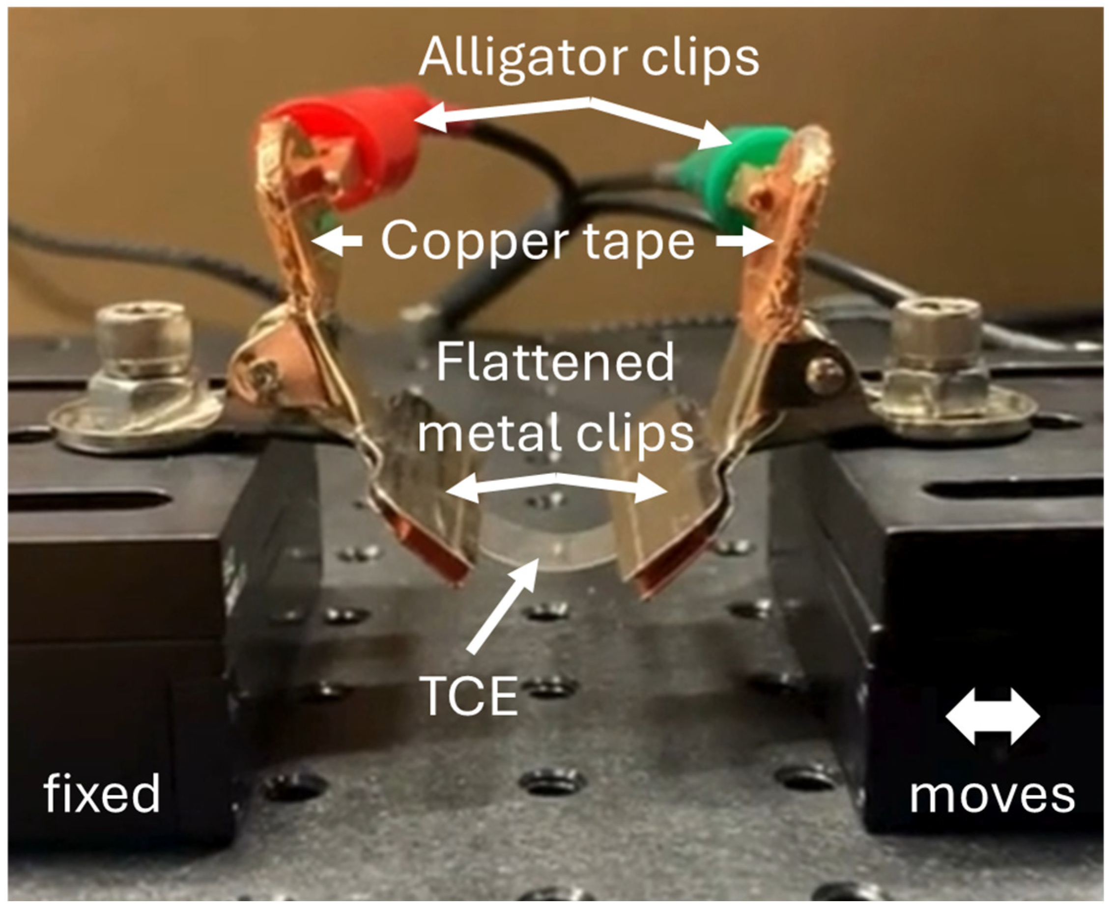
Hybrid TCEs are fabricated using PET substrates with Ag MBLs. Multiple layers of AgNWs are printed using an anilox with 8.5 BCMI with 180 LPI and a smooth print plate in succession after a 90 s relax time with a two-minute 90 °C drying step between layers to ensure all solvents are evaporated before printing other layers. Two layers of IZO are printed using an anilox with 5.8 BCMI with 500 LPI, advanced 03 print plate, 2.3 N/cm anilox line contact pressure, 1.3 N/cm print line contact pressure, 70% anilox speed, and 12 m/min print speed. After a 90 s relax time, a two-minute 90 °C drying step is completed after each IZO layer. After all layers are printed, the samples are photonically cured, rinsed with DI water, and blown dry with nitrogen. Unless specified, our typical hybrid TCE samples consist of three layers of AgNWs and two layers of IZO, regardless of the AgNW ink composition.

2.7. Bending Test

The mechanical durability of hybrid TCEs and PET/ITO from Sigma-Aldrich are tested using the custom bending testing unit shown in Figure 1. Samples used for bending tests are cut into 13 mm × 50 mm sizes. The bending test apparatus is built with two flattened Coideal metal hinge clips mounted on Thorlabs PT1 micrometer-controlled translation stages. The left stage is fixed in position, and the right stage is motorized using a Thorlabs Z925B actuator controlled by a Thorlabs KDC101 brushed motor controller. Both clips have a thin strip of room-temperature vulcanizing silicone on the top clamps to secure the sample and a strip of copper tape on the lower clamps to ensure good electrical contact with the TCE sample. An additional copper tape is adhered to the handles to reduce contact resistance to the alligator clips connected to the Keithley 2635B source measure unit (SMU) for resistance measurements. A sample is securely held between the metal clips with the TCE in contact with the lower clamps so that when the sample bends, the TCE layer is under tension (Figure 1). The clips are placed 15 mm apart, so when the translational stage moves the clips to a 10 mm separation between them, the sample bends to a 5 mm radius. Strain applied to the hybrid TCE layer or ITO on PET substrates is calculated as shown in previous studies using the thickness of the substrate, the thickness of the layer of interest, and the bending radius [29]. Each sample undergoes 2000 cycles of bending from a 7.5 mm bending radius to a 5.0 mm bending radius. The strain applied to the hybrid TCE layer cycles between 0.6% and 1.0%, while the strain cycles between 0.8% and 1.3% for the ITO on the PET from Sigma-Aldrich. Resistance is measured when the sample is at its original position after every 10 bending cycles (R) and normalized to the value before any bending cycles (R0) until 2000 bending cycles are completed. A custom code using Python Pycharm Version 3.10 controls the actuator to move the sample and record the resistance measurements.

2.8. MAPbI3 PSC Fabrication and Testing

Methylammonium lead iodide (MAPbI3) PSCs are fabricated on 1 inch x 1 inch hybrid TCEs. The flexible substrates are mounted onto a thin, rigid piece of glass (0.5 mm) for device fabrication and handling. The p-i-n device architecture is composed of hybrid TCE/neutral PEDOT:PSS/PEDOT:PSS/MeO-2PACz/MAPbI3/PCBM/bathocuproine (BCP)/Al/Ag. The hole transport layer (HTL) is fabricated by first spin-coating neutral PEDOT:PSS (pH = 7) on the hybrid TCE, followed by spin-coating regular PEDOT:PSS (pH = 1.7) on top of the neutral PEDOT:PSS layer [30]. The spin-coating conditions for both layers are 4000 RPM for 30 s; annealing at 120 °C for 10 min is performed after depositing each layer. Next, MeO-2PACz (4 mg/mL in ethanol) is spin-coated on top of the neutral PEDOT:PSS/PEDOT:PSS layer at 3000 RPM for 30 s and annealed at 100 °C for 10 min. Details on the preparation of regular PEDOT:PSS and neutral PEDOT:PSS have been previously reported [30]. The anti-solvent-free MAPbI3 precursor solution is prepared inside a nitrogen-filled glovebox by dissolving an equal molar ratio of PbI2 and MAI in 2-MOE (0.8 M) and adding NMP (40 mol % of MAPbI3) [31]. The MAPbI3 precursor solution is mixed for at least 3 h before use. HTL-coated TCE substrates and MAPbI3 precursor solution are transferred into a nitrogen-purged glovebox with less than 3% relative humidity. The MAPbI3 film is made by depositing the precursor solution onto the spinning substrate at 5000 RPM for 20 s, followed by annealing on a hot plate at 100 °C for 10 min. Next, PCBM (20 mg/mL in chlorobenzene) is spin-coated at 1200 RPM for 60 s, followed by spin-coating BCP (0.5 mg/mL in ethanol) at 4000 RPM for 30 s. Finally, 100 nm of Al and 50 nm of Ag are thermally evaporated in a nitrogen glovebox as top contacts. The diode size is 0.11 cm2, and the illumination aperture size is 0.0491 cm2. The final devices are stored in the nitrogen glovebox overnight before current density–voltage (J-V) measurements. The J-V measurements are performed under an AM 1.5G 100 mW cm−2 AAA solar simulator (Abet) in a nitrogen glovebox using a Keithly 2635A source meter. The applied voltage is varied from 1.2 V to −0.2 V for the reverse scan and from −0.2 V to 1.2 V for the forward scan with a scan speed of 70 mV s−1.

3. Results and Discussion

3.1. AgNW Morphology

3.1.1. Print Parameters

We first examine how print parameters affect the AgNW morphology after one layer of AgNWs (Figure 2). Higher magnification images for each condition in Figure 2 are shown in Figure S4 in the Supplementary Materials File to better depict how AgNWs are distributed. Figure 2a,b compare the print line contact pressure when using a patterned print plate (Advance 04 print plate). Figure 2a shows AgNWs printed with 11.6 N/cm print line contact pressure, while Figure 2b is made using 1.2 N/cm print line contact pressure. The same AgNW ink is used for all images in Figure 2 and Figure S4; therefore, the different morphologies between the images are caused by the print parameters. The black spots are large AgNW agglomerations in Figure 2 and appear white in Figure S4 when using a high mag objective lens. The large AgNW agglomerations are the result of AgNWs being lodged into the soft print plate grooves before being transferred to the substrate. The results show that lower print line contact pressure minimizes AgNW agglomeration. Figure 2c,d compare patterned vs. smooth print plates. In both cases, the same amount of AgNW ink is used while the print force is kept at the same setting (10 N), although the line contact pressure differs by 0.8 N/cm due to the difference in cross-web dimension for the patterned vs. smooth print plate. Figure 2c shows fewer AgNWs due to fewer AgNWs being transferred from the patterned print plate to the substrate. This can be clearly seen in Figure S4c. Figure 2c has smaller clusters of AgNWs, and Figure 2d has larger area clusters, indicating that AgNW spreading is better when printing with a smooth print plate because the AgNWs are not caught in the cells of the patterned print plate. The effects of anilox volume are compared in Figure 2e (5.8 BCMI with 502 LPI) and f (8.5 BCMI with 180 LPI), both using a smooth print plate. The higher BCMI anilox has deeper, larger-width cells that can hold more AgNW ink. Using the higher BCMI anilox results in a higher density of AgNWs on the substrate compared to the lower BCMI anilox. Figure 2c,e might appear to be more uniform than their counterparts (Figure 2d,f), but looking at higher magnification optical images shown in Figure S4 in the Supplementary Materials File, it is evident there are fewer AgNWs on the substrate. Figure 2g,h demonstrate the effect of print speed: 30 m/min (Figure 2h) produces a more uniform AgNW layer compared to 12 m/min (Figure 2g). These results establish that the aggregation of printed AgNWs is reduced with a lower print force, smooth print plate, an anilox with a higher BCMI (and lower LPI), and a faster printing speed.
For the remainder of the manuscript, AgNW prints are made with the lowest possible print force governed by the ink viscosity and print speed to ensure the print plate does not slip when in contact with the substrate. Typically, to print the AgNW layers, a smooth print plate is used with print parameters of 5 N/cm anilox line contact pressure, 80% anilox speed, and 30 m/min print speed. The anilox line contact pressure is kept at 5 N/cm to ensure the print plate and anilox do not skip during the printing process. The anilox speed is given as a percentage of the print speed, here kept at 80% to prevent ink drying on the surface of the anilox before transferring to the print plate. We find that the anilox speed does not affect the print quality. While increasing the print speed from 12 to 30 m/min results in a more uniform AgNW layer, faster speeds do not further improve the print quality.

3.1.2. Solvent Engineering

Gravure inks are designed for a specific viscosity, surface tension, boiling point, and surface energy to enable efficient ink transfer and formation of a uniform film [32]. In this study, the AgNW ink is transferred from the anilox to the smooth print plate and then to the substrate. The AgNW ink needs to be carefully optimized because the anilox roller, print plate, and substrate have different topographies and surface energies, and the AgNW ink is transferred twice. We use a previous study that printed AgNWs with direct gravure as a guide [20]. Details on shear rates and ink transfer physics have been extensively studied in a review article [19].
To optimize ink, we compare AgNW ink as received in IPA (5 mg/mL) with inks containing 10% 1-butanol or 10% DI water. After printing a wet film, the evaporation of the solvent is determined by its vapor pressure, which is different for these three solvents (IPA: 4.4 kPa, 1-butanol: 0.93 kPa, DI water: 2.4 kPa at 25 °C). Another important characteristic time is the time for the wet film to spread uniformly on the surface, also known as leveling time. Derived from the Navier–Stokes equation, the leveling time (τ), τ = 3ηλ4/16π4γh3, is proportional to the viscosity (η) and inverse to the surface tension (γ) [33]. The viscosity values for the three solvents are IPA 2.43 mPa·s, 1-butanol: 2.57 mPa·s, DI water: 1 mPa·s, and the surface tension values are IPA: 22 mN/m, 1-butanol: 25 mN/m, DI water: 72 mN/m. To estimate a leveling time, wet film thickness modulations with a wavelength (λ) are assumed, as well as a resulting uniform thickness (h) if given sufficient leveling time. Using η and γ for AgNW ink found in previous studies [17,20], a λ of 500 µm (estimated from Figure 2h) and an estimated h of 4 microns [34], a leveling time for the AgNWs films is estimated to be ~200 milliseconds, which is shorter than the time for all the solvent to evaporate observed in our experiment. However, the ink viscosity increases with the progression of solvent drying, so before all the solvent is evaporated, the AgNWs settle on the substrate, and their distribution becomes ‘frozen’. In consideration of these factors, 1-butanol added as a co-solvent to the AgNW ink only aids in film uniformity by reducing the rate of drying. Adding DI water not only reduces the rate of drying but also induces faster leveling through lower viscosity and higher surface tension.
Figure 3 shows optical images of substrates that contain three layers of AgNWs. The sample printed from as-received AgNW ink (Figure 3a) shows large “ribbing” patterns (indicated by red lines in Figure 3) caused by the high viscosity and low surface tension of the IPA. “Ribbing” refers to high-density and low-density AgNW areas parallel to the printing direction and is attributed to the Saffman–Taylor instability [35]. The ribbing feature could be further exacerbated if the AgNW ink dries during the pre-inking step, which increases AgNW concentration and thereby increases viscosity. Ribbing is observed to be shorter for AgNWs printed using ink containing 10% 1-butanol (Figure 3b). This observation could be attributed to the fact that adding 1-butanol only slows down the evaporation of the co-solvent (IPA and 1-butanol) ink because AgNW spreading does not change substantially due to similar viscosity and surface tension of IPA and 1-butanol. Also, because less evaporation occurs, the concentration of AgNWs and ink viscosity remain constant during the pre-inking step. We find the ribbing problem is reduced the most when using the ink containing 10% DI water (Figure 3c). Using a simple rule of mixtures without considering solvent interaction, the AgNW ink with 10% DI water has a 6% lower viscosity and a 22% higher surface tension. Since the leveling time is linearly proportional to viscosity and inversely proportional to surface tension, the leveling time reduces correspondingly. The combination of lower viscosity, higher surface tension, and lower vapor pressure ensures the mixed solvents do not evaporate before leveling. Since DI water has both lower vapor pressure and higher surface tension than IPA in this mixed solvent system, it is also possible that local gradients in solvent composition could accelerate leveling via Marangoni flows [36].

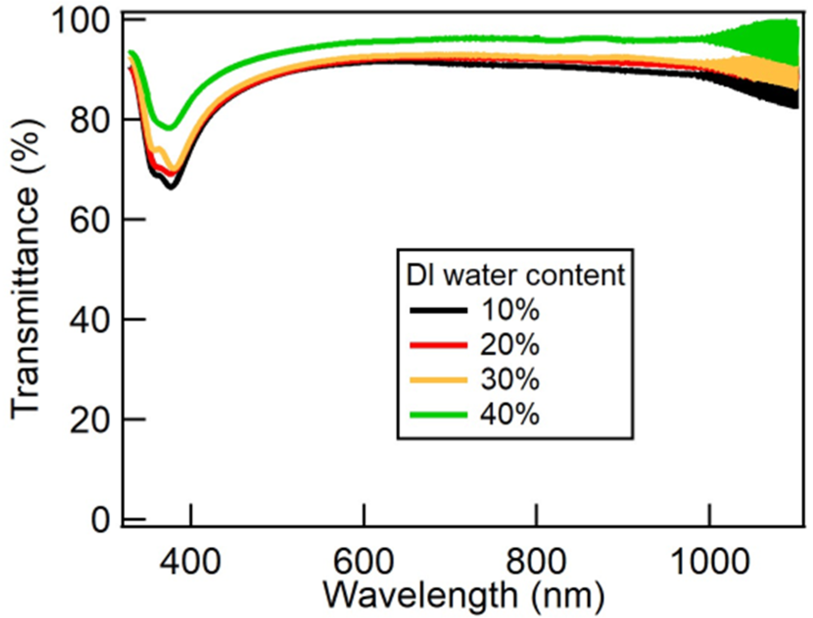
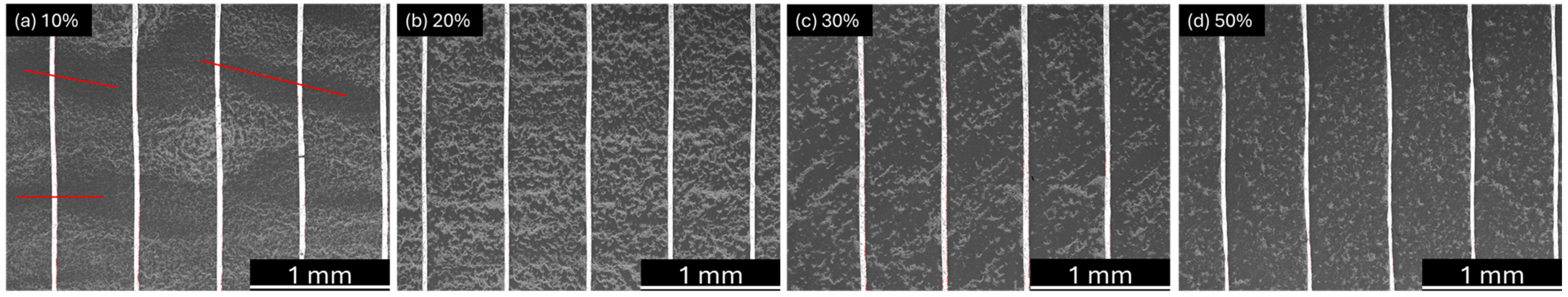
3.2. Optimized DI Water Concentration for Hybrid TCE Fabrication

Further optimization of DI water concentration in the ink is based on the properties of hybrid TCEs, which are fabricated by printing three layers of AgNWs with a smooth print plate and printing two layers of IZO. PET/Ag MBL substrates are printed with three prints of AgNWs from inks with 10%, 20%, 30%, and 50% DI water concentrations. The AgNW concentration is not held constant for the inks but decreases with increasing amounts of DI water. After the IZO is printed and dried, the samples are photonically cured with the 2 J/cm2 condition in a stationary position. Transmittance spectra of hybrid TCE samples made with varying DI water content are shown in Figure 4. Transmittance averaged between 400 and 1100 nm (Tavg) and Rsh for the hybrid TCEs are shown in Table 2. Hybrid TCEs made from AgNW inks with 10%, 20%, or 30% DI water show slight increases in both Tavg and Rsh values that reflect lower AgNW concentrations in inks containing more DI water. However, the Tavg and Rsh values for these three samples overlap, indicating that the multiscale AgNW network is formed even at 30% DI water. When the AgNW ink is diluted with 50% DI water, the Tavg is 4–6% higher, and the Rsh is twice that of the other AgNW inks. Consistent with our previous results using spin coating [12] and blade coating [15], the higher Tavg values are the results of fewer AgNWs due to the water dilution, and the higher Rsh indicates that fewer AgNW junctions are present.
To examine the large-scale uniformity of these hybrid TCEs, laser images are shown in Figure 5 for a single layer of AgNWs printed on PET/Ag MBL substrates using AgNW inks with varying DI water content. Using 10% DI water content in the AgNW ink shows ribbing (Figure 5a red lines), similar to what is shown in Figure 3. The AgNW network is more uniform when 20% DI water is used due to the increased time available for AgNWs to distribute before the film becomes dry (Figure 5b). When the water content is 30%, the AgNWs ribbing is not observed, but the AgNWs are agglomerated (Figure 5c). A possible explanation for the agglomeration of AgNWs in the film made with 30% DI water content in the AgNW ink is that AgNWs cannot distribute in the wet film properly due to higher surface tension, as explained in a previous study [20]. Figure 5d shows that when using AgNW ink with 50% DI water content, the AgNW distribution is uniform but with a low concentration of AgNWs. Even after printing 5 layers of AgNWs from 50% DI water AgNW ink, only an Rsh of 21 Ω/sq is achieved. Printing many layers will slow down an R2R manufacturing line, and therefore, 50% DI water is not desired for printing AgNWs.
Prints from AgNW inks with 20% DI water exhibit the best uniformity of the AgNW network, and this 20% DI water AgNW ink is used for further investigation into photonic curing, solar cell fabrication, and scaling up. Table S2 shows the optical, electrical, and physical properties of the resulting hybrid TCEs. Samples photonically cured at 477 V (3.6 J/cm2) have similar but slightly better Tavg, Rsh, haze, σRMS, and d values compared to those processed at 350 V (2 J/cm2). An AFM image for a hybrid TCE photonically cured with the 477 V condition is given in the Supplementary Materials File (Figure S5). The roughness of these samples is ~15 nm. We previously showed that ~60 nm of IZO was needed to completely cover the AgNWs and reduce the roughness below 5 nm [15]. Thus, the roughness of these samples is consistent with the fact that IZO thicknesses are not sufficient to smooth out the AgNW morphology. The 477 V photonic curing condition is used to make hybrid TCEs for mechanical durability testing, photonic curing at speed to show R2R compatibility, and MAPbI3 PSCs.

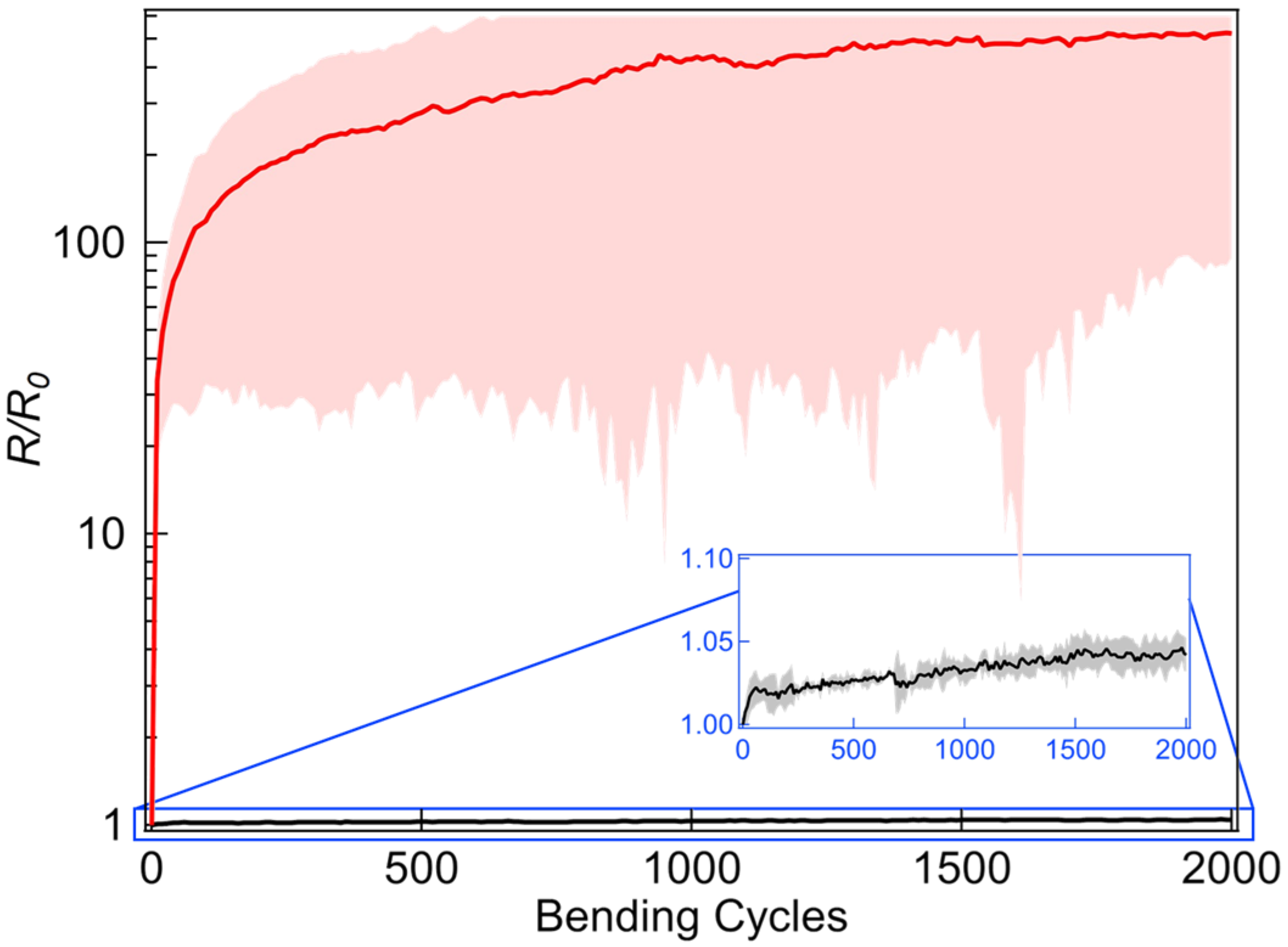
3.3. Mechanical Durability of Hybrid TCE

Three samples of gravure printed hybrid TCEs and Sigma-Aldrich (SA) PET/ITO are bent to a radius of 5 mm, shown in Figure 6 as black and red curves, respectively. Using a bending radius of 5 mm applies a maximum strain of 1.0% to the hybrid TCE layer on the PET and 1.3% to the ITO layer on the PET for SA PET/ITO. The resistance ratio (R/R0, where R0 is the initial resistance) of the gravure-coated hybrid TCEs increases less than 5% after 2000 cycles, as shown in the inset with a zoom-in y scale in Figure 6. The R/R0 of SA PET/ITO samples in Figure 6 increases ~ 90% to 1000% after 2000 cycles. The large standard deviation of SA PET/ITO samples is indicative of high sample variability. The bending test results confirm the gravure-printed hybrid TCE is robust and will not degrade from being wound on rollers during R2R manufacturing.

3.4. Compatibility with R2R

Next, we demonstrate making hybrid TCE samples at speeds compatible with high-throughput manufacturing for both deposition and annealing. Figure 7a shows an image of a 10 cm (cross-web) × 20 cm (down-web) hybrid TCE, the largest continuous area that can be fabricated using the IGT F1-100. Longer samples have gaps due to the print plate being fixed on the printing wheel by electrical tape. The samples are photonically cured in web-sync mode using the 477 V condition. Figure 7b shows Tavg and Rsh measurements across the sample. The measurements in green boxes (Figure 7b) correspond to the locations of green circles in Figure 7a. The hybrid TCE shown in Figure 7 has a relative uniformity of 2% in Tavg and 12% in Rsh over the whole sample, clearly showing good process control.
If all deposition and processing steps can be completed at a single web speed, only a single R2R line of equipment is needed, reducing capital expenditure. The optimized TCEs in Section 3.2 are fabricated by printing AgNWs at 30 m/min, IZO at 12 m/min, and photonically curing at 7 m/min. To ensure all hybrid TCE fabrication steps can be performed at the same speed, IZO is printed at 30 m/min. All other print parameters are kept the same as printing IZO at 12 m/min and are given in the Methods Section. The printed film showed large-area uniformity (Figure S6). The sample also has a low standard deviation in transmittance of 0.5% measured over the 10 cm × 10 cm sample in four different locations. Therefore, AgNWs and IZO can be printed at 30 m/min using gravure printing. Next, we examine how to increase photonic curing speed. For a given photonic curing condition (pulse length, lamp voltage, number of pulses, number of micro-pulses, and duty cycle), the web speed can be increased by using larger power supplies [23]. Using SimPulse version 3.1.0.1, a thermal simulation software developed for the PulseForge tool family, a web speed of 43 m/min is possible when using 55 A of current from 110 A power supplies for the same lamp and lamp drivers we used. Therefore, all steps of the hybrid TCE fabrication process can be performed on a single R2R line at 30 m/min web speed.

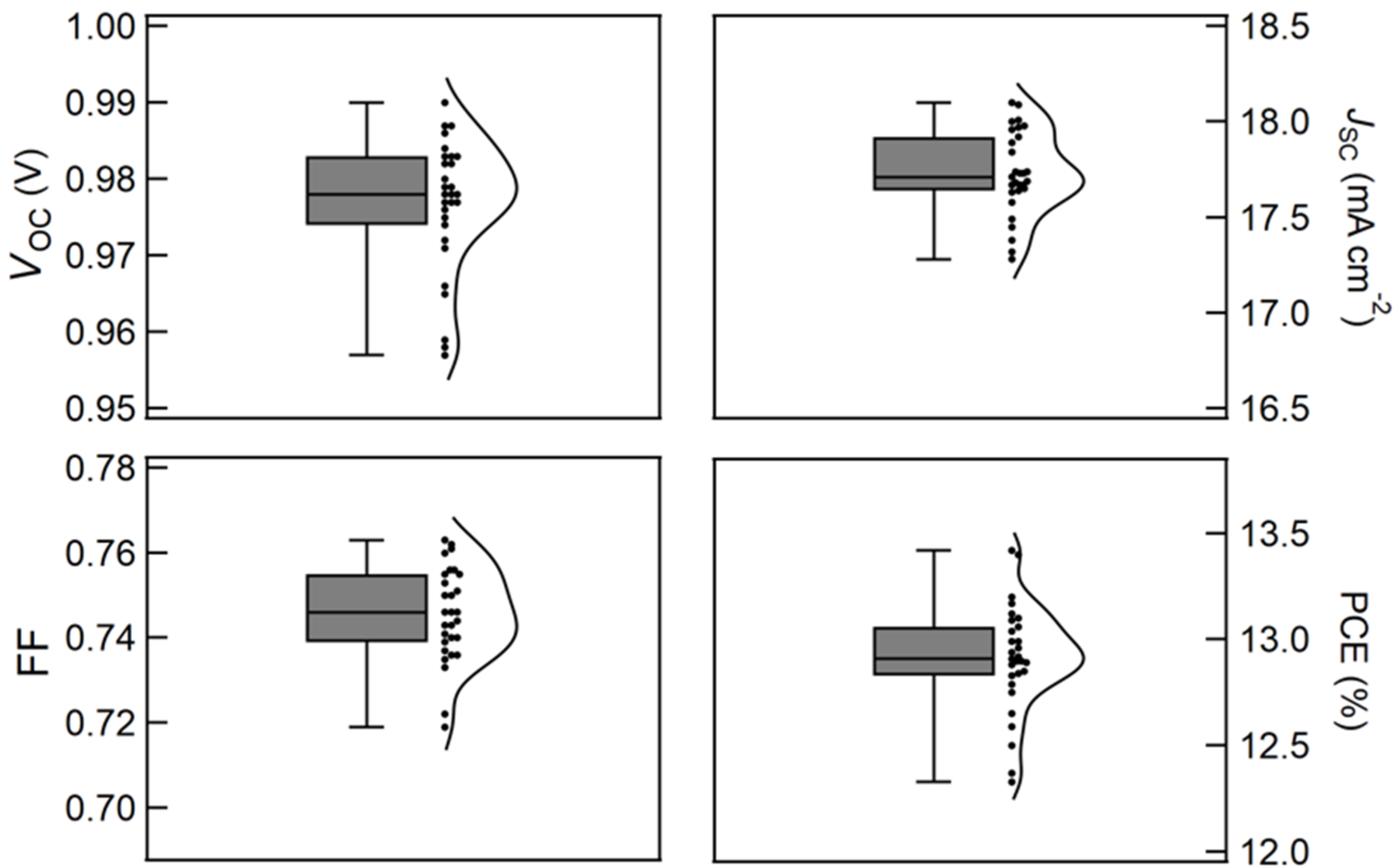
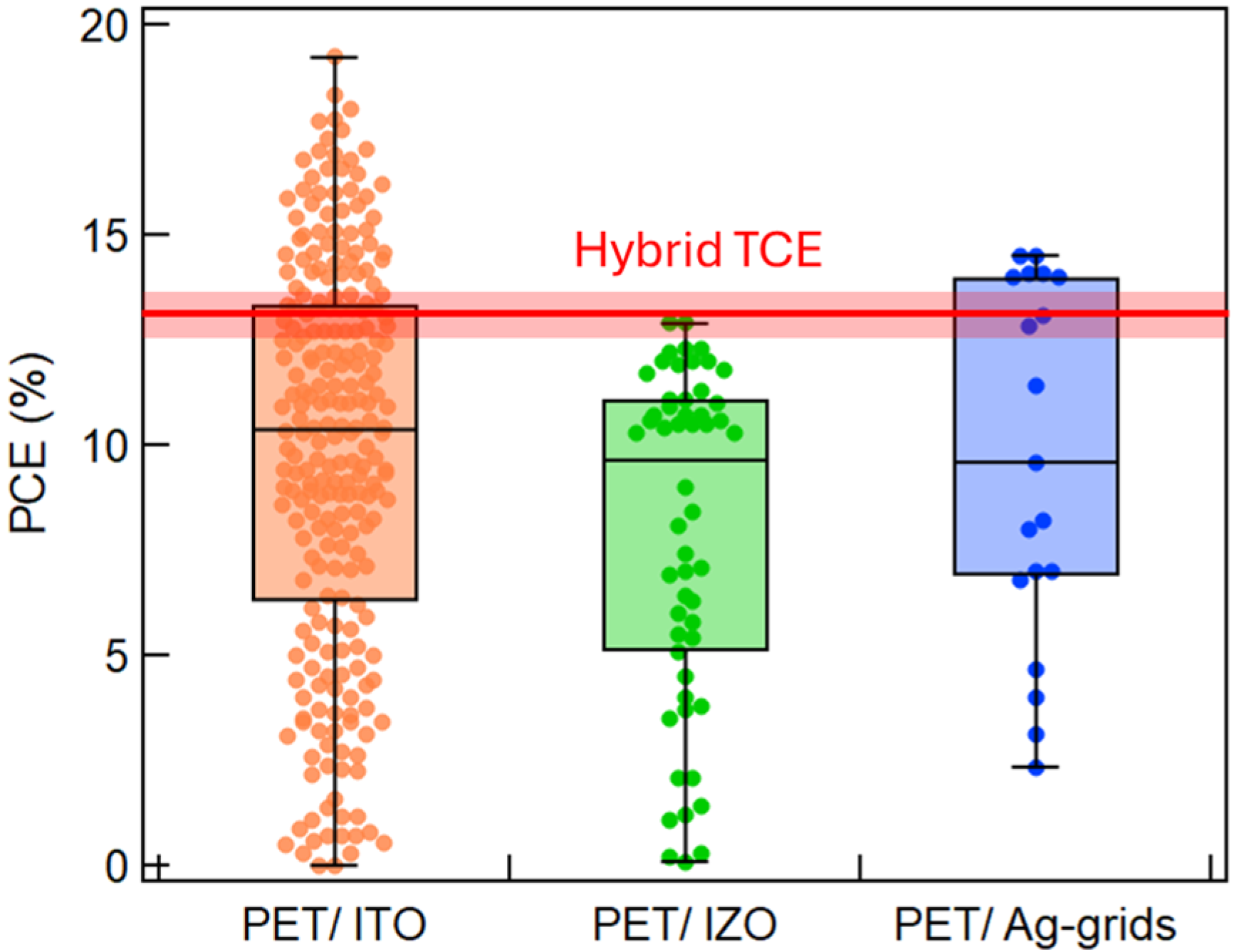
3.5. PSC Device Performance

MAPbI3 PSCs are fabricated on hybrid TCEs to confirm their superior performance for thin-film solar cell applications. Figure 8 shows box plots of J-V parameters obtained from 15 devices. Hysteresis in forward and reverse scans is minimal or non-existent in these devices, as shown in Figure S7 for the champion device. MAPbI3 PSCs fabricated on the hybrid TCEs achieve an average open-circuit voltage (Voc) = (0.98 ± 0.01) V, short-circuit current density (Jsc) = (17.7 ± 0.2) mA/cm2, fill factor (FF) = (0.75 ± 0.01), and power conversion efficiency (PCE) = (13 ± 0.3) %. Figure 9 shows the MAPbI3 PSCs fabricated on hybrid TCEs compared to those fabricated on PET/ITO, PET/IZO, and PET/Ag-grids documented in an open database [37]. While higher-performing MAPbI3 PSCs have been reported on PET/ITO, the average PCE of 13% is among the best-performing MAPbI3-based PSCs on other PET substrates reported in the literature, as shown in Figure 9. The small variation in the J-V parameters of the PSCs made on the hybrid TCEs further confirms that uniform, high-quality TCEs can be produced using R2R-compatible deposition methods and photonic curing on PET.

4. Conclusions

Developing scalable solution deposition and processing methods is key to lowering the cost of TCEs through increased manufacturing throughput. This work shows the fabrication of hybrid TCEs on PET/Ag MBL substrates using gravure printing for AgNWs and IZO layers and photonic curing to process the stack. Using offset gravure printing and adding water to the AgNW ink, AgNWs improved network uniformity with lower print forces, smooth print plate, and higher print speed. Hybrid TCEs are successfully fabricated using entirely R2R scalable methods, achieving Tavg = (92 ± 2)%, Rsh = (11.4 ± 0.3) Ω/sq, haze = (4.4 ± 0.2)%, d = (31 ± 5) nm, and a surface roughness of (15.2 ± 1.8) nm. The process is scaled to large samples and photonically cured in an R2R tool at 7 m/min, achieving a relative uniformity of 2% in Tavg and 12% in Rsh. Mechanical durability tests using a custom bending apparatus show the resistance increases by <5% after 2000 cycles of bending to a tensile strain of 1.0%, indicating that the hybrid TCEs are robust and suitable for winding on rollers during R2R manufacturing. The state-of-the-art MAPbI3 PSCs, with an average PCE of (13 ± 0.3) %, are achieved on the hybrid TCEs. We further show that all deposition and processing steps can be completed at 30 m/min, proving their manufacturability using R2R. This work establishes a pathway to fully R2R-compatible fabrication of TCEs on inexpensive PET substrates for thin-film solar cell applications, facilitating high-throughput PSC manufacturing.

Supplementary Materials

The following supporting information can be downloaded at: https://www.mdpi.com/article/10.3390/nanomanufacturing5020005/s1, Figure S1: SEM image of Cheap Tubes AgNWs on Si substrate; Figure S2: IGT F1-100 gravure printing machine; Figure S3: AniCam image of the surface of anilox with 8.5 BCMI; Table S1: Anilox details; Figure S4: High magnification optical images of a single layer of AgNWs gravure printed on PET/Ag MBL substrates. Table S2: Properties of Hybrid TCEs photonically cured using different conditions; Figure S5: AFM scan of the surface of a hybrid TCE made with the 477 V condition; Figure S6: Low magnification optical image of PET/MBL substrate with IZO printed at 30 m/min; Figure S7: Forward and reverse J-V curves for the champion MAPbI3 PSC made on hybrid TCEs.

Author Contributions

J.C.B.: Data curation, Formal analysis, Investigation, Methodology, Software, Validation, Visualization, Writing—original draft, Writing—review and editing; B.B.: Data curation, Formal analysis, Investigation, Methodology, Software, Validation, Visualization, Writing—review and editing; G.J.V.S.: Investigation, Methodology, Writing—review and editing; G.B.: Investigation; K.A.S.: Investigation; J.E.H.: Investigation; W.J.S.: Methodology, Validation, Writing—review and editing; J.W.P.H.: Conceptualization, Validation, Funding Acquisition, Methodology, Project Administration, Resources, Supervision, Writing—review and editing. All authors have read and agreed to the published version of the manuscript.

Funding

This work was funded by the U.S. Department of Energy’s Office of Energy Efficiency and Renewable Energy under the Solar Energy Technologies Office Award Numbers DE-EE0009518 and DE-EE00011153. This report was prepared as an account of work sponsored by an agency of the United States Government. Neither the United States Government nor any agency thereof, nor any of their employees, makes any warranty, express or implied, or assumes any legal liability or responsibility for the accuracy, completeness, or usefulness of any information, apparatus, product, or process disclosed, or represents that its use would not infringe privately owned rights. Reference herein to any specific commercial product, process, or service by trade name, trademark, manufacturer, or otherwise does not necessarily constitute or imply its endorsement, recommendation, or favoring by the United States Government or any agency thereof. The views and opinions of authors expressed herein do not necessarily state or reflect those of the United States Government. G.B. acknowledges the support for Research Experiences for Undergraduates under the National Science Foundation Award CMMI-2135203. J.E.H. was supported by a U.S. Department of Education Graduate Assistance in Areas of National Need (GAANN) fellowship from the Department of Education. The contents of this work do not necessarily represent the policy of the Department of Education, and one should not assume endorsement by the Federal Government. J.W.P.H. acknowledges the support of the Texas Instruments Distinguished Chair in Nanoelectronics.

Data Availability Statement

All data shown in this manuscript are available upon request from the corresponding author.

Acknowledgments

The authors would like to thank Energy Materials Corporation for providing PET/MBL substrates, M. Davis for laser scribing hybrid TCEs for thickness measurements, S. Christensen for his aid during TCE fabrication, and C. Hazboun for preliminary hybrid TCE characterization.

Conflicts of Interest

Author Garrett J. Vander Stouw is an employee of Energy Materials Corporation. Author Kurt A. Schroder is an employee of PulseForge, Inc. The remaining authors declare that the research was conducted in the absence of any commercial or financial relationships that could be construed as a potential conflict of interest.

References

  1. Ellmer, K. Past Achievements and Future Challenges in the Development of Optically Transparent Electrodes. Nat. Photonics 2012, 6, 809–817. [Google Scholar] [CrossRef]
  2. Lee, H.B.; Jin, W.-Y.; Ovhal, M.M.; Kumar, N.; Kang, J.-W. Flexible Transparent Conducting Electrodes Based on Metal Meshes for Organic Optoelectronic Device Applications: A Review. J. Mater. Chem. C 2019, 7, 1087–1110. [Google Scholar] [CrossRef]
  3. Nguyen, V.H.; Papanastasiou, D.T.; Resende, J.; Bardet, L.; Sannicolo, T.; Jiménez, C.; Muñoz-Rojas, D.; Nguyen, N.D.; Bellet, D. Advances in Flexible Metallic Transparent Electrodes. Small 2022, 18, 2106006. [Google Scholar] [CrossRef]
  4. Piper, R.T.; Xu, W.; Hsu, J.W.P. How Optical and Electrical Properties of ITO Coated Willow Glass Affect Photonic Curing Outcome for Upscaling Perovskite Solar Cell Manufacturing. IEEE J. Photovoltaics 2022, 12, 722–727. [Google Scholar] [CrossRef]
  5. Azani, M.; Hassanpour, A.; Torres, T. Benefits, Problems, and Solutions of Silver Nanowire Transparent Conductive Electrodes in Indium Tin Oxide (ITO)-Free Flexible Solar Cells. Adv. Energy Mater. 2020, 10, 2002536. [Google Scholar] [CrossRef]
  6. Weng, Y.; Chen, G.; Zhou, X.; Zhang, Y.; Yan, Q.; Guo, T. Stability Enhancement and Patterning of Silver Nanowire Networks by Conformal TiO2 Coating for Flexible Transparent Conductive Electrodes. J. Mater. Sci. 2023, 58, 17816–17828. [Google Scholar] [CrossRef]
  7. Li, P.; Ma, X.; Gong, G.; Xu, C.; Zhang, Z. Room-Temperature, Solution-Processed, Robust, Transparent, and Conductive SiO x /AgNW Nanocomposite Coating. ACS Appl. Mater. Interfaces 2024, 16, 43724–43733. [Google Scholar] [CrossRef] [PubMed]
  8. Gerlein, L.F.; Benavides-Guerrero, J.A.; Cloutier, S.G. Photonic Post-Processing of a Multi-Material Transparent Conductive Electrode Architecture for Optoelectronic Device Integration. RSC Adv. 2024, 14, 4748–4758. [Google Scholar] [CrossRef]
  9. Liu, W.; Hu, Y.; Chen, Y.; Hu, Z.; Zhou, K.; Min, Z.; Liu, H.; Zhan, L.; Dai, Y. Improvement of Electrical Properties of Silver Nanowires Transparent Conductive by Metal Oxide Nanoparticles Modification. Coatings 2022, 12, 1816. [Google Scholar] [CrossRef]
  10. Im, H.-G.; Jang, J.; Jeon, Y.; Noh, J.; Jin, J.; Lee, J.-Y.; Bae, B.-S. Flexible Transparent Crystalline-ITO/Ag Nanowire Hybrid Electrode with High Stability for Organic Optoelectronics. ACS Appl. Mater. Interfaces 2020, 12, 56462–56469. [Google Scholar] [CrossRef]
  11. Yu, S.; Liu, X.; Dong, H.; Wang, X.; Li, L. Flexible High-Performance SnO2/AgNWs Bilayer Transparent Conductors for Flexible Transparent Heater Applications. Ceram. Int. 2021, 47, 20379–20386. [Google Scholar] [CrossRef]
  12. Piper, R.T.; Xu, W.; Hsu, J.W.P. Silver Nanowire-Indium Zinc Oxide Composite Flexible Transparent Conducting Electrodes Made by Spin-Coating and Photonic Curing. MRS Adv. 2023, 8, 177–182. [Google Scholar] [CrossRef]
  13. Arulkumar, S.; Senthilkumar, T.; Parthiban, S.; Dharmalingam, G.; Goswami, A.; Alshehri, S.M.; Gawande, M.B. AgNWs-a-TiOx: A Scalable Wire Bar Coated Core–Shell Nanocomposite as Transparent Thin Film Electrode for Flexible Electronics Applications. J. Mater. Sci. Mater. Electron. 2021, 32, 6454–6464. [Google Scholar] [CrossRef]
  14. Zhang, Y.; Bai, S.; Chen, T.; Yang, H.; Guo, X. Facile Preparation of Flexible and Highly Stable Graphene Oxide-Silver Nanowire Hybrid Transparent Conductive Electrode. Mater. Res. Express 2020, 7, 16413. [Google Scholar] [CrossRef]
  15. Bonner, J.C.; Piper, R.T.; Bhandari, B.; Allen, C.R.; Bower, C.T.; Ostendorf, M.A.; Davis, M.; Valdez, M.; Lee, M.; Hsu, J.W.P. “Green” Fabrication of High-Performance Transparent Conducting Electrodes by Blade Coating and Photonic Curing on PET for Perovskite Solar Cells. Mater. Sustain. 2024, 1, 1. [Google Scholar] [CrossRef]
  16. Alsaid, D.A.; Rebrosova, E.; Joyce, M.; Rebros, M.; Atashbar, M.; Bazuin, B. Gravure Printing of ITO Transparent Electrodes for Applications in Flexible Electronics. J. Disp. Technol. 2012, 8, 391–396. [Google Scholar] [CrossRef]
  17. Scheideler, W.J.; Smith, J.; Deckman, I.; Chung, S.; Arias, A.C.; Subramanian, V. A Robust, Gravure-Printed, Silver Nanowire/Metal Oxide Hybrid Electrode for High-Throughput Patterned Transparent Conductors. J. Mater. Chem. C 2016, 4, 3248–3255. [Google Scholar] [CrossRef]
  18. EMC. High Speed Inline Roll-to-Roll Module Production. Available online: https://enmatcorp.com/high-speed-inline-roll-to-roll-module-production/ (accessed on 15 May 2024).
  19. Grau, G.; Cen, J.; Kang, H.; Kitsomboonloha, R.; Scheideler, W.J.; Subramanian, V. Gravure-Printed Electronics: Recent Progress in Tooling Development, Understanding of Printing Physics, and Realization of Printed Devices. Flex. Print. Electron. 2016, 1, 23002. [Google Scholar] [CrossRef]
  20. Wang, Z.; Han, Y.; Yan, L.; Gong, C.; Kang, J.; Zhang, H.; Sun, X.; Zhang, L.; Lin, J.; Luo, Q.; et al. High Power Conversion Efficiency of 13.61% for 1 Cm 2 Flexible Polymer Solar Cells Based on Patternable and Mass-Producible Gravure-Printed Silver Nanowire Electrodes. Adv. Funct. Mater. 2021, 31, 2007276. [Google Scholar] [CrossRef]
  21. Huang, Q.; Zhu, Y. Gravure Printing of Water-Based Silver Nanowire Ink on Plastic Substrate for Flexible Electronics. Sci. Rep. 2018, 8, 15167. [Google Scholar] [CrossRef]
  22. Daunis, T.B.; Schroder, K.A.; Hsu, J.W.P. Photonic Curing of Solution-Deposited ZrO2 Dielectric on PEN: A Path towards High-Throughput Processing of Oxide Electronics. npj Flex. Electron. 2020, 4, 7. [Google Scholar] [CrossRef]
  23. Schroder, K.A.; Martin, K.M.; Jackson, D.K.; McCool, S.C. Method and Apparatus for Curing Thin Films on Low-Temperature Substrates at High Speeds. U.S. Patent No. 9, 095, 874 B2, 4 August 2014. [Google Scholar]
  24. Hsu, J.W.P.; Piper, R.T. Photonic Curing for Innovative Fabrication of Flexible Metal Oxide Optoelectronics. J. Phys. D Appl. Phys. 2024, 57, 252001. [Google Scholar] [CrossRef]
  25. Lee, M.; Piper, R.T.; Bhandari, B.; Hsu, J.W.P. Multiobjective Optimization of Silver-Nanowire Deposition for Flexible Transparent Conducting Electrodes. ACS Appl. Nano Mater. 2023, 6, 17364–17368. [Google Scholar] [CrossRef]
  26. Sigma, M. Indium Tin Oxide Coated PET. Available online: https://www.sigmaaldrich.com/US/en/product/aldrich/639303 (accessed on 1 June 2023).
  27. CheapTubes.com. Silver Nanowires 30 nm OD. Available online: https://www.cheaptubes.com/product/silver-nanowires-30nm/ (accessed on 1 June 2023).
  28. Kim, M.G.; Kanatzidis, M.G.; Facchetti, A.; Marks, T.J. Low-Temperature Fabrication of High-Performance Metal Oxide Thin-Film Electronics via Combustion Processing. Nat. Mater. 2011, 10, 382–388. [Google Scholar] [CrossRef]
  29. Gunda, M.; Kumar, P.; Katiyar, M. Review of Mechanical Characterization Techniques for Thin Films Used in Flexible Electronics. Crit. Rev. Solid State Mater. Sci. 2017, 42, 129–152. [Google Scholar] [CrossRef]
  30. Bhandari, B.; Bonner, J.C.; Piper, R.T.; Hsu, J.W.P. Effects of Transparent Conducting Electrodes and Hole Transport Layers on the Performance of MAPbI 3 Solar Cells Fabricated on PET Substrates. Flex. Print. Electron. 2024, 9, 35002. [Google Scholar] [CrossRef]
  31. Lee, S.H.; Hong, S.; Kim, H.J. Selection of a Suitable Solvent Additive for 2-Methoxyethanol-Based Antisolvent-Free Perovskite Film Fabrication. ACS Appl. Mater. Interfaces 2022, 14, 39132–39140. [Google Scholar] [CrossRef] [PubMed]
  32. Hernandez-Sosa, G.; Bornemann, N.; Ringle, I.; Agari, M.; Dörsam, E.; Mechau, N.; Lemmer, U. Rheological and Drying Considerations for Uniformly Gravure-Printed Layers: Towards Large-Area Flexible Organic Light-Emitting Diodes. Adv. Funct. Mater. 2013, 23, 3164–3171. [Google Scholar] [CrossRef]
  33. Huddy, J.E.; Ye, Y.; Scheideler, W.J. Eliminating the Perovskite Solar Cell Manufacturing Bottleneck via High-Speed Flexography. Adv. Mater. Technol. 2022, 7, 2101282. [Google Scholar] [CrossRef]
  34. Chen, Y.-R.; Hong, C.-C.; Liou, T.-M.; Hwang, K.C.; Guo, T.-F. Roller-Induced Bundling of Long Silver Nanowire Networks for Strong Interfacial Adhesion, Highly Flexible, Transparent Conductive Electrodes. Sci. Rep. 2017, 7, 16662. [Google Scholar] [CrossRef]
  35. Saffman, P.G.; Taylor, G. The Penetration of a Fluid into a Porous Medium or Hele-Shaw Cell Containing a More Viscous Liquid. Proc. R. Soc. Lond. A Math. Phys. Sci. 1958, 245, 312–329. [Google Scholar]
  36. Huddy, J.E.; Scheideler, W.J. Engineering Ink Rheology for Boosting Efficiency of Large-Area Flexography-Printed Perovskite Solar Cells. In Proceedings of the 2024 IEEE 52nd Photovoltaic Specialist Conference (PVSC), Seattle, WA, USA, 9–14 June 2024; pp. 483–485. [Google Scholar]
  37. Jacobsson, T.J.; Hultqvist, A.; García-Fernández, A.; Anand, A.; Al-Ashouri, A.; Hagfeldt, A.; Crovetto, A.; Abate, A.; Ricciardulli, A.G.; Vijayan, A.; et al. An Open-Access Database and Analysis Tool for Perovskite Solar Cells Based on the FAIR Data Principles. Nat. Energy 2021, 7, 107–115. [Google Scholar] [CrossRef]
Figure 1. Bending test apparatus with a TCE sample held in place by two metal clips. The right clip is attached to a movable stage controlled by an actuator. The TCE is only the bottom side contacting copper tape. Copper tape on the flattened metal clips lowers contact resistance for resistance measurements. The alligator clips are connected to an SMU for resistance measurements.
Nanomanufacturing 05 00005 g001
Figure 2. Optical images of a single layer of AgNWs gravure printed on PET/Ag MBL (vertical lines) substrates. Printing with a patterned print plate, 8.5 BCMI anilox with 180 LPI, 2.3 N/cm anilox line contact pressure, and 12 m/min print speed, the print line contact pressure is (a) 11.6 N/cm and (b) 1.2 N/cm. Using an 8.5 BCMI anilox with 180 LPI, 50 N anilox set force, 10 N print set force, and print speed of 12 m/min, the print plate is (c) patterned and (d) smooth. The line contact pressures corresponding to anilox force and print force are 5.8 N/cm and 1.2 N/cm, respectively, for (c) and 5 N/cm and 1 N/cm, respectively, for (d). Printing using a smooth print plate, 5 N/cm anilox force, 1.5 N/cm print force, and print speed of 12 m/min, anilox volume is (e) 5.8 BCMI with 502 LPI and (f) 8.5 BCMI with 180 LPI. Printing using a smooth print plate, 8.5 BCMI anilox with 180 LPI, 5 N/cm anilox line contact pressure, 1.5 N/cm print line contact pressure, the print speed is (g) 12 m/min and (h) 30 m/min.
Nanomanufacturing 05 00005 g002
Figure 3. Optical images of three AgNW layers printed from (a) as-received AgNW ink in IPA, (b) 10% 1-butanol in AgNW ink, and (c) 10% DI water in AgNW ink. Red lines in each image show the middle of observed ribbing features.
Nanomanufacturing 05 00005 g003
Figure 4. UV-Vis transmittance spectra of hybrid TCEs containing three AgNW layers made from IPA AgNW ink with 10% (black line), 20% (red line), 30% (orange line), and 50% (green line) DI water.
Nanomanufacturing 05 00005 g004
Figure 5. Laser images of one layer of AgNWs made using (a) 10%, (b) 20%, (c) 30%, and (d) 50% DI water in the AgNW ink. Red lines indicate ribbing in (a). The vertical lines are PET/Ag MBLs.
Nanomanufacturing 05 00005 g005
Figure 6. Logarithmic scale of R/R0 for three samples of gravure-printed hybrid TCE (black) and Sigma-Aldrich (SA) PET/ITO (red) for 2000 bending cycles at a radius of 5 mm (tensile strain of 1.0% and 1.3%, respectively). Resistance is measured every 10 cycles for 2000 cycles. The solid line represents the averaged data, and the shaded area represents the standard deviation between the samples (N = 3) for each case. The inset shows the zoom-in linear R/R0 plot of the gravure-printed hybrid TCE.
Nanomanufacturing 05 00005 g006
Figure 7. (a) Camera image of a hybrid TCE made using 20% DI water AgNW ink and photonically cured in the web-synched mode in an R2R system. (b) Tavg and Rsh values measured at locations marked with green circles in (a).
Nanomanufacturing 05 00005 g007
Figure 8. Box plots of the J-V parameters (forward and reverse scan) of 15 MAPbI3 PSCs fabricated on hybrid TCEs. The bottom and top of the boxes represent the 25th and 75th percentiles, with the line in the middle representing the median. Whiskers extend to the minimum and maximum values, and the dots represent individual data points.
Nanomanufacturing 05 00005 g008
Figure 9. Box plots comparing MAPbI3 PSCs fabricated on PET/ITO (orange), PET/IZO (green), and PET/Ag-grids (blue). The average (solid) and standard deviation (shaded) for PCE of MAPbI3 PSCs on our hybrid TCEs made by gravure coating and photonic curing are shown as a red line. The data for PET/ITO, PET/IZO, and PET/Ag-grids are taken from an open-access database [37].
Nanomanufacturing 05 00005 g009
Table 1. Review of the literature on TCEs fabricated by overcoating AgNWs with metal oxide. The deposition and annealing methods for AgNWs and the metal oxide are given, as well as the substrate and reference. For AgNWs and metal oxide deposited with different methods, the two methods are given and separated by “/”. The annealing temperature is the external temperature provided by the apparatus, not the temperature the sample reached.
Metal Oxide OvercoatingDeposition MethodAnnealing Method (Temperature)SubstrateReference
TiO2, SnO2, Al2O3, ZnOspin coating/sputteringhot plate (100 °C)“ceramic substrate”[9]
ITOspray coating/sputteringhot plate (250 °C)resin and glass fiber[10]
SnO2spin coating/sputteringnonePET[11]
TiO2spin coating/sputteringhot plate (130 °C)PDMS[6]
IZOspin coating/spin coatingphotonic curing
(room temperature)
PET[12]
Amorphous TiOxbar coatinghot plate (100 °C)glass[13]
Graphene
Oxide
Meyer rodhot plate (110 °C)PET[14]
SiOxknife coating or spin coatingvacuum UV irradiation (80 °C)PET[7]
TiO2spin coatingphotonic curing
(room temperature)
PET[8]
IZOblade coatingphotonic curing (room temperature)PET[15]
ITOgravure printing/patterned and etchedOven (120 °C)PET[16]
IZOgravure printinghot plate (up to 300 °C) or
tube furnace (325 °C)
glass and PEN[17]
Table 2. Tavg and Rsh values for hybrid TCEs with three layers of AgNWs made with varying DI water contents, two layers of IZO, and photonically cured at 350 V (2 J/cm2).
DI Water Content (%)Tavg (%)Rsh (Ω/sq)
108910.3 ± 0.6
209012.2 ± 0.2
309112.7 ± 0.6
509528.7 ± 1.4
Disclaimer/Publisher’s Note: The statements, opinions and data contained in all publications are solely those of the individual author(s) and contributor(s) and not of MDPI and/or the editor(s). MDPI and/or the editor(s) disclaim responsibility for any injury to people or property resulting from any ideas, methods, instructions or products referred to in the content.

