1. Introduction
Recently, the rapid advancement of modern technology has driven an unprecedented proliferation of portable electronic devices. Products such as smartphones, tablets, and wearable gadgets are no longer considered luxuries but have become indispensable tools for communication, productivity, and entertainment in daily life. As these systems continue to evolve, consumer expectations demand ever-higher levels of performance, faster data-processing speeds, and lower power consumption. Among the critical factors influencing the overall system efficiency, memory technologies play a pivotal role. The capacity, speed, and endurance of memory directly determine the responsiveness, stability, and user experience of portable electronics. Therefore, the development of advanced memory devices with enhanced characteristics is of fundamental importance in both industry and academia.
To satisfy the stringent requirements of next-generation electronic systems, memory must exhibit a combination of high storage density, fast operational efficiency, ultra-low power consumption, and long-term reliability. Conventional charge-based memories, such as dynamic random access memory and flash memory, are increasingly facing scaling limitations and performance bottlenecks as device dimensions approach the nanoscale. These challenges have prompted extensive research into emerging non-volatile memory technologies capable of overcoming the limitations of traditional memory architectures.
Among the various candidates, resistive random access memory (RRAM) has emerged as one of the most promising technologies due to its unique material properties and simple device configuration. RRAM offers several significant advantages: it is inherently non-volatile, meaning it can retain stored information even in the absence of power; it demonstrates extremely low write power consumption compared to flash memory; and it features a small unit cell area, enabling highly scalable and three-dimensional integration for ultra-dense memory arrays. Structurally, RRAM is remarkably straightforward. The bagadolinium device can be realized by inserting a thin insulating layer between two conductive electrodes. Typically, noble metals or highly conductive materials are used as the top and bottom electrodes, while the insulating layer is composed of high dielectric constant materials, most commonly transition metal oxides such as TiO2, HfO2, Al2O3, or Ta2O5.
The switching mechanism relies on the application of an external bias voltage across the device, which induces a localized change in the resistance state of the insulating layer. This change is attributed to the formation and rupture of conductive filaments or to valence change mechanisms involving oxygen vacancies and metal cation migration. As a result, the device can toggle between a high-resistance state (HRS) and a low-resistance state (LRS), effectively encoding digital “0” and “1” information.
Beyond its fundamental operation, RRAM also offers several additional advantages relevant to future applications. It demonstrates fast switching speed (often in the nanosecond regime), excellent endurance across multiple switching cycles, and compatibility with complementary metal-oxide-semiconductor back-end-of-line processes. Moreover, its capability for multi-level resistance states opens the door for high-density storage, as well as novel computing paradigms such as in-memory computing and neuromorphic systems, whose aim to mimic biological synaptic functions for artificial intelligence applications.
The combination of simplicity in device structure, favorable material properties, and advanced functionality positions RRAM as a leading candidate for the next generation of universal memory. It addresses the limitations of conventional memory technologies but also provides opportunities to enable new computational architectures tailored for the rapidly expanding fields of edge computing, IoT, and machine learning hardware [
1,
2,
3,
4,
5,
6,
7,
8,
9,
10,
11,
12,
13,
14].
2. Experiment
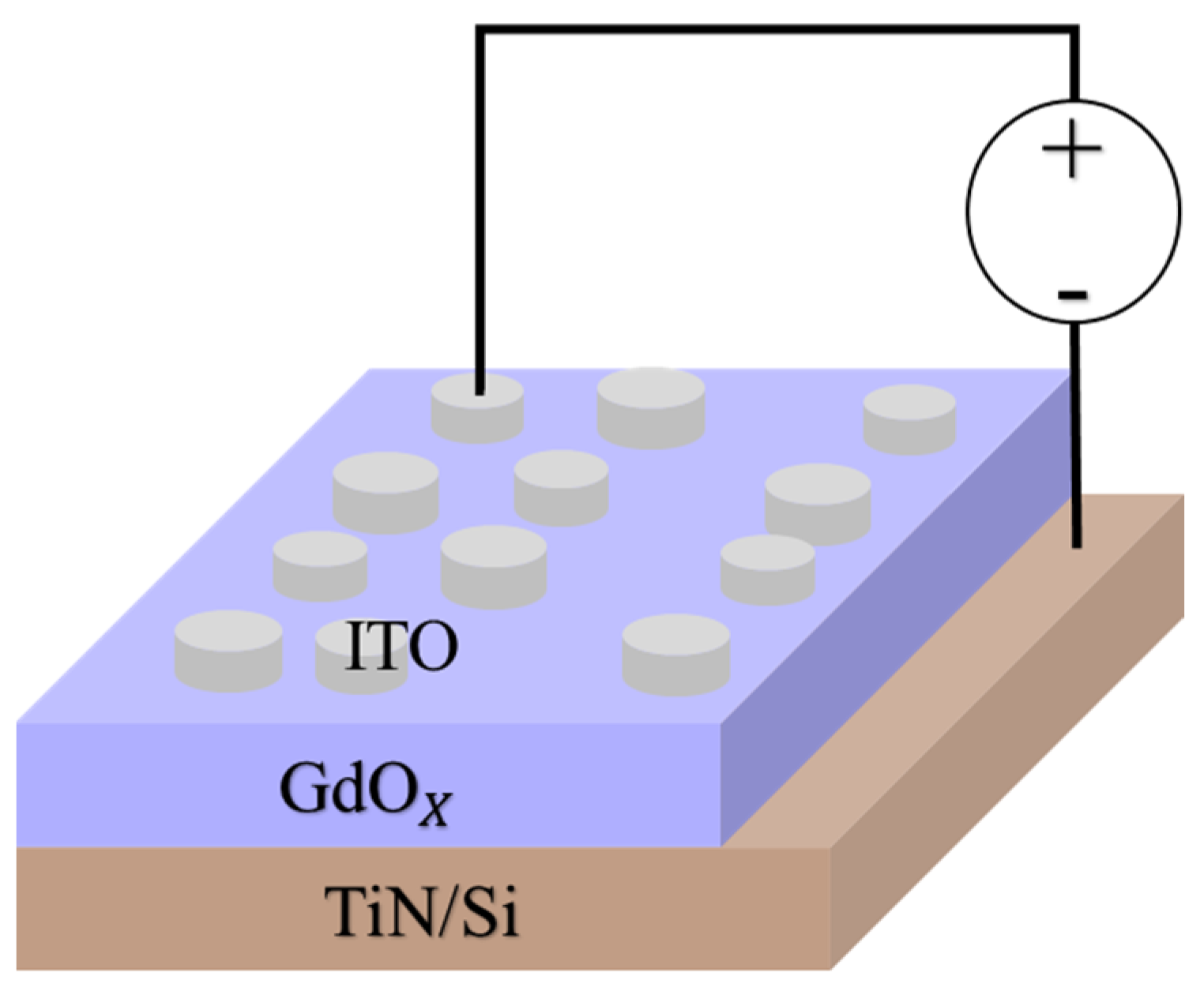
We used radio frequency (RF) magnetron sputtering to deposit gadolinium oxide (GaO) thin films with different oxygen concentrations on TiN/Si substrates as the insulating layer of the resistive memory. Then, different annealing temperatures and supercritical fluids are used to change the characteristics of the test piece. Finally, a metal mask is covered, and indium tin oxide (ITO) is deposited as the top electrode through sputtering to form a metal electrode/oxide layer/metal electrode (M-I-M) structure (
Figure 1). The insulating layer parameters are shown in
Table 1, and the top electrode parameters are shown in
Table 2. The prepared resistive memory element is then measured using a current-voltage (I-V) curve measurement software-controlled precision power measurement device (B2902B) to measure its electrical properties and find the optimal parameters.
Table 1 summarizes the sputtering parameters of gadolinium thin films deposited under different power conditions. These parameters, including power level, working pressure, gas flow ratio, and deposition rate, are crucial for optimizing film uniformity, density, and stoichiometry. The electrical reliability and switching performance of RRAM devices are strongly dependent on these deposition variables, as they determine the defect density, interface quality, and conduction mechanism pathways within the switching layer.
In this study, the reaction was carried out in a pure carbon dioxide chamber heated to 120 °C and at a pressure of 3000 psi. The supercritical carbon dioxide fluid passivated the defects and reduced the defect density, thereby improving the film quality and reducing the degradation rate of the resistive memory element, thereby improving the durability of the element and other characteristics.
3. Result and Discussion
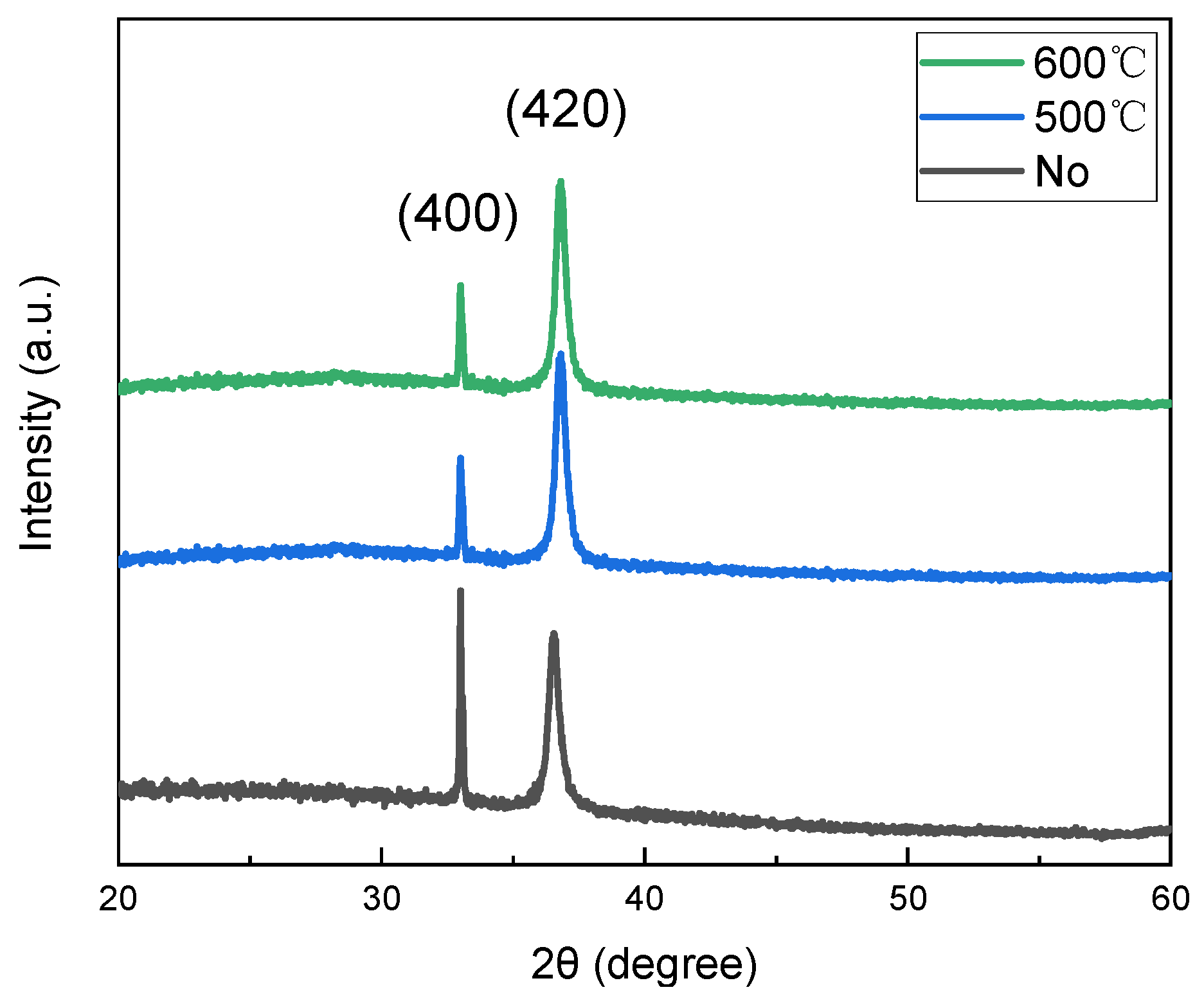
Figure 2 shows the X-ray diffraction (XRD) pattern of 15 min/Ar:O2 = 10:0. The corresponding data show that the peaks of gadolinium are at 33 and 37 °C, and their crystal phases correspond to (400) and (420), respectively, with atomic spacing of 2.7 and 2.4 Å. The peak of the annealed sample at (400) decreases, and the peak at (420) increases, indicating that the atomic spacing is shortened and the atomic arrangement is denser. The half-height width is improved after annealing. The grain size of the unannealed sample is 91 and 14.6 nm, 44.5 and 17.2 nm after annealing at 500 °C, and 48.1 and 16.5 nm after annealing at 600 °C. The resistor layer film is a polycrystalline material. After rapid high-temperature treatment, smaller grains are formed. The film has fewer voids, which reduces the scattered electron flow and resistivity.
Film thickness is a critical parameter in thin-film device fabrication, as it directly influences the structural, electrical, and functional properties of resistive switching devices. In this study, the thickness of the deposited films was quantitatively determined using an alpha-step surface profilometer, which provides high-resolution step-height measurements by mechanically scanning across the film/substrate interface. This method enables precise correlation between the deposition time and the resulting film thickness, thereby allowing us to establish the deposition rate under specific sputtering conditions.
To examine the dependence of film growth on deposition duration, thin films were deposited at a constant RF sputtering power of 50 W while varying the sputtering time. The measured film thicknesses were as follows: after 15 min, the thickness was approximately 105.3 Å; after 30 min, the thickness increased significantly to 385.5 Å; and after 45 min, the thickness reached 585.6 Å. These results indicate a non-linear growth behavior, which is attributed to the initial nucleation stage of film formation followed by a more stable deposition regime as the sputtering time increases. The experimental data are used to estimate the average deposition rate and evaluate the influence of surface morphology evolution on electrical performance.
Following film deposition, the electrical characteristics of the fabricated devices were evaluated under post-deposition treatments, namely rapid thermal annealing (RTA) and supercritical fluid treatment. These treatments are known to significantly modify the microstructure, defect states, and interfacial quality of oxide or carbide-based switching layers, thereby influencing resistive switching behavior.
The electrical measurements revealed the following key device parameters, set voltage (
V_SET) of 2.9 V, reset voltage (
V_RESET) of 2.3 V, leakage current of on the order of 10
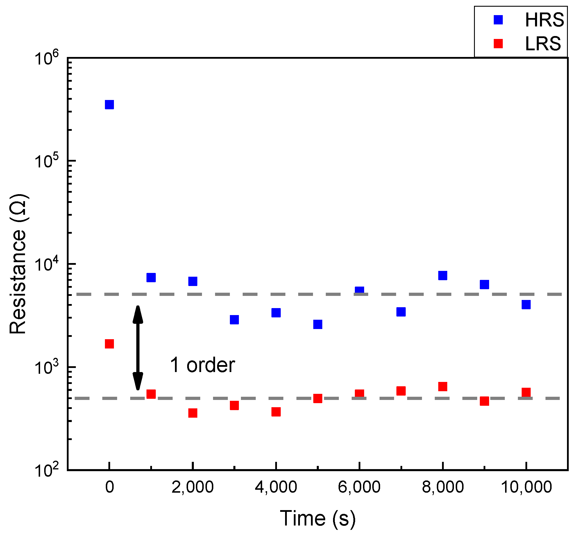
−6 A, compliance current limit of 5 mA (to prevent permanent dielectric breakdown), read voltage of 0.15 V, on/off resistance ratio: approximately 2 at initial measurements, and endurance performance: stable switching for more than 1800 cycles. However, retention analysis demonstrated that as the measurement duration increased to 10
4 seconds, the on/off ratio degraded significantly and could only be maintained at approximately one order of magnitude (
Figure 3). This decline indicates the presence of unstable conductive filaments or relaxation of oxygen vacancy distributions over time, both of which accelerate resistance state collapse.
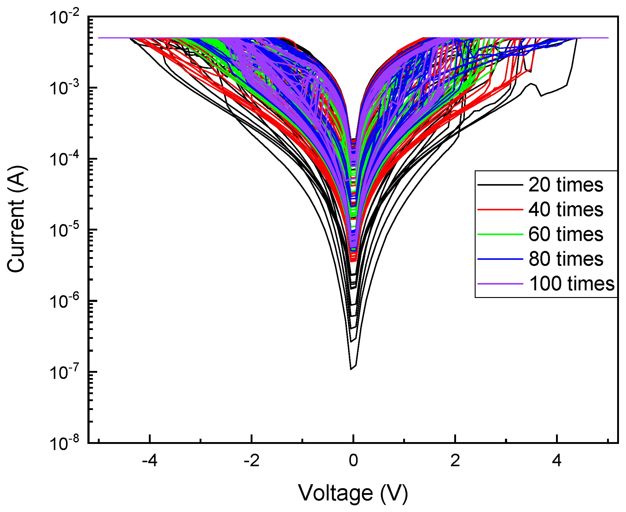
The I-V characteristics depicted in
Figure 4 confirm the degradation of continuous switching performance. Initially, the switching behavior was distinguishable between HRS and LRS, but with repeated cycling, the separation between states became less stable, and the resistance window deteriorated more rapidly. Such degradation is a common reliability concern in RRAM devices, often linked to localized Joule heating, structural relaxation, and stochastic filamentary dynamics.
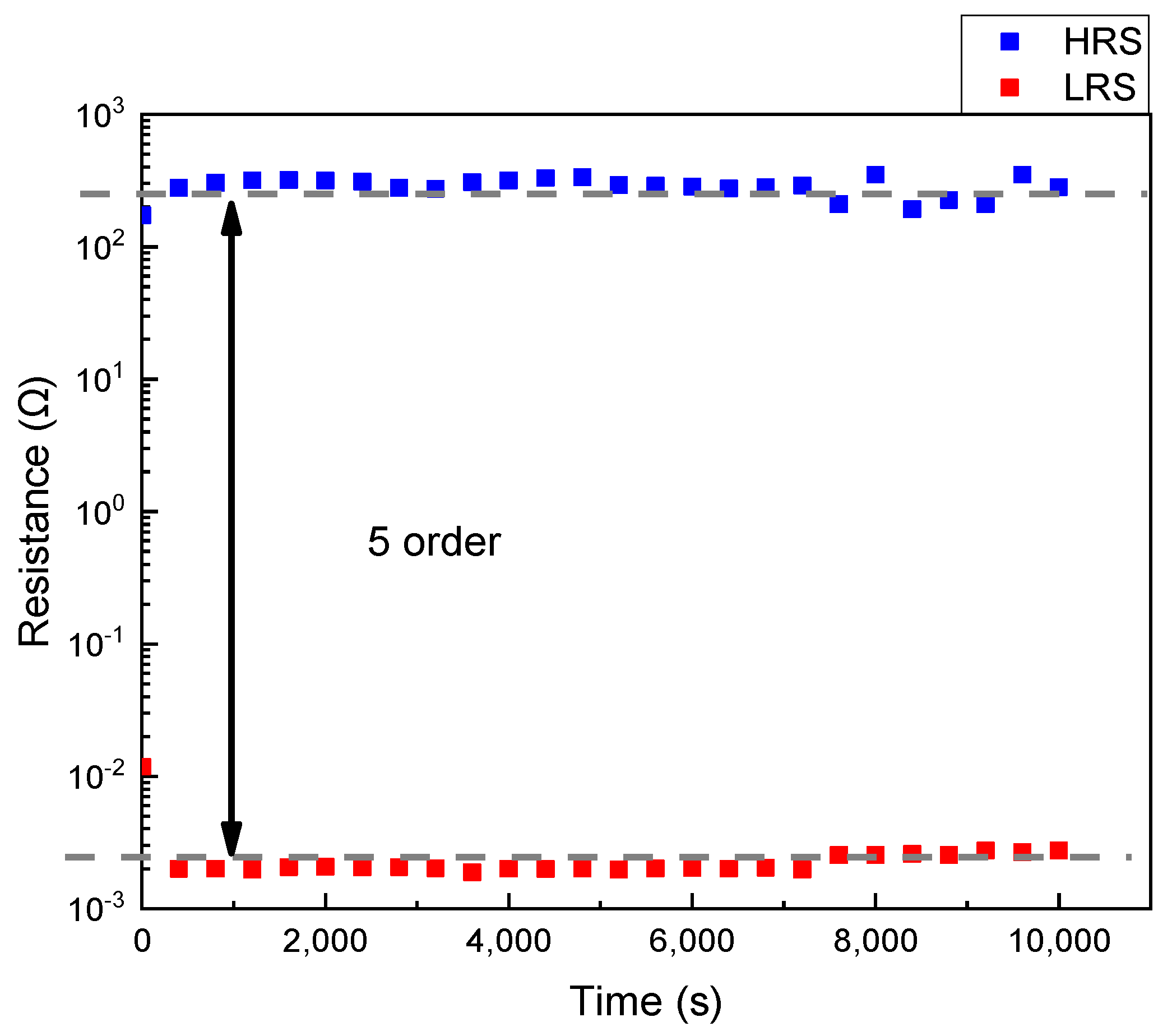
In
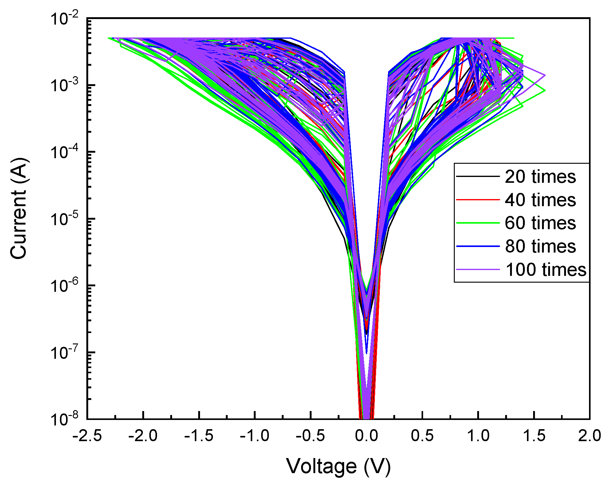
Figure 5, the retention properties of the RTA-treated GdO films RRAM devices were also shown. In contrast, the switching ratio of the supercritical fluid (SCF)-treated film is five times that of the former. The set voltage is 1.2 V, the reset voltage is −1.0 V, the low resistance value switched during the process reaches several milliohms, and the high resistance value is hundreds of ohms, as shown in
Figure 6.
Figure 6 is a stack of the 100-time curves; it has a high overlap and always maintains a fixed switching ratio and operating voltage. The maximum cycle number of switching exceeds 5000 times.
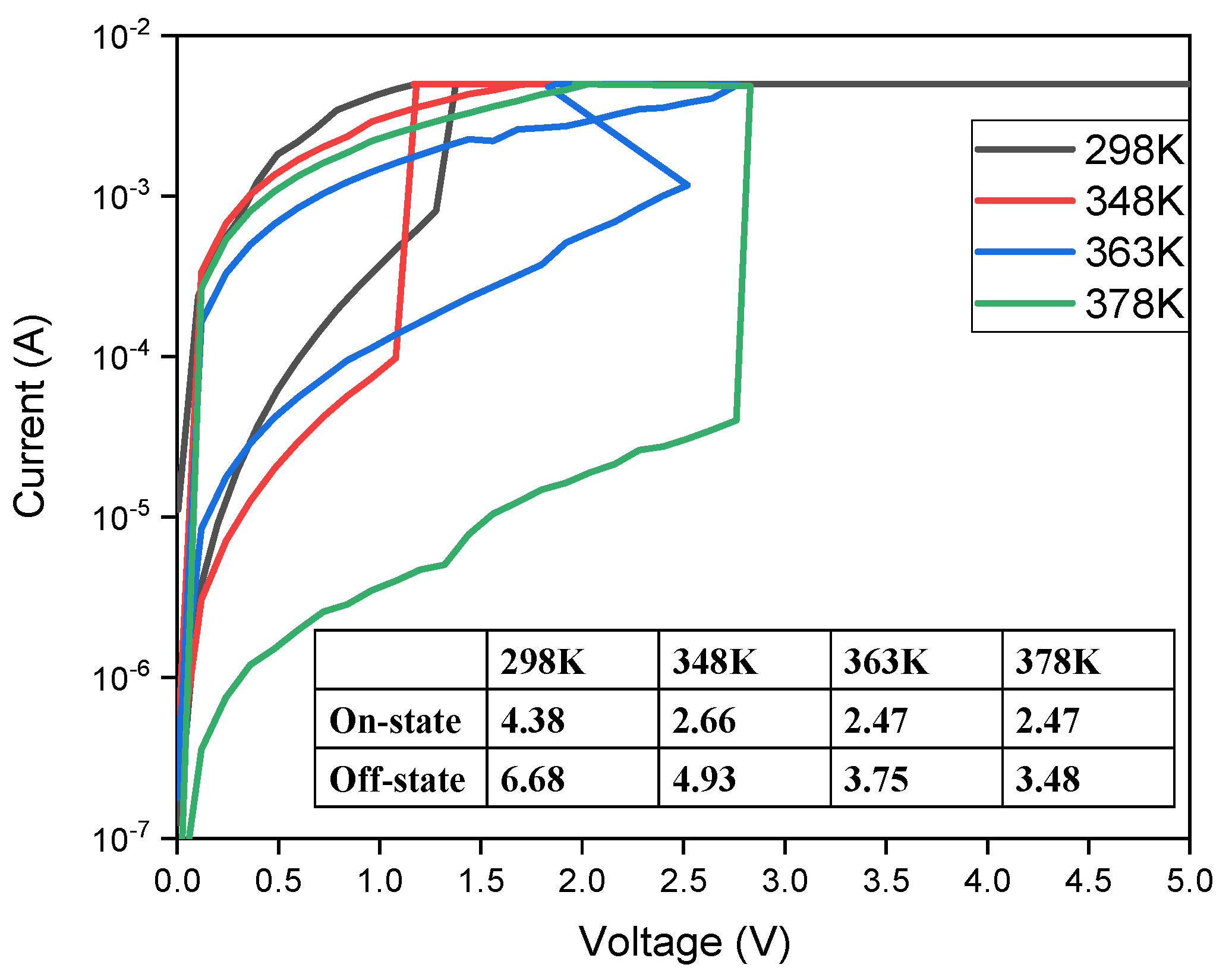
When bias is applied to the resistive memory, oxygen ions move upward. At this time, the ions need to pass through the interface between the dielectric layer and the electrode above the energy barrier height to form a barrier wire that penetrates the ITO electrode. There is an energy barrier height at the interface between the metal and the insulating layer. The energy barrier of the interface is crossed by external heat energy, allowing electrons to pass through the insulator’s conduction band. The change in the Schottky barrier height at 25 °C, 75 °C, 90 °C, and 105 °C is measured by heating. The high-resistance energy barrier height in
Figure 7 drops from 6.68 to 3.48 eV. As the temperature rises, the external thermal energy lowers the Schottky energy barrier, so more ions can cross the interface, but it also causes the operating voltage to increase. This is because too many oxygen ions enter ITO and fill its internal vacancies, causing the energy gap of ITO to increase, so a higher voltage is required to allow electrons to pass through.
4. Conclusions
Using RF magnetron sputtering technology, we prepared thin films on titanium nitride substrates. GdO thin films are deposited at a single power of 50 W with a sputtering time of 15 min. Indium tin oxide with the same parameters is plated on the dielectric film as the top electrode to form an MIM resistive memory. The film properties and performance are improved through heat treatment and supercritical fluid treatment, and then electrical analysis is performed to obtain the optimal parameters and explain the changes in phygadoliniumal properties, and then the optimal parameters are tested for retention.
The film deposition quality is poor because there is no substrate heating and no thermal annealing during the coating process, which makes the conductive path unable to be stably formed and broken, resulting in poor measurement results. In terms of thickness, the longer the deposition time of the film, the more oxygen vacancies are needed to form a resistive wire. The thinner the film, the more obvious the characteristics of oxygen deposition are. After heat treatment, the best characteristics are shown by annealing at 600 °C with a thickness of 10 and 60 nm. The former has a switch ratio of about two orders, an operating voltage of about 1.5 V, a leakage current of about 10
−6 A, and a continuous operation number of more than 1.3 × 10
3 times. The high-resistance state conduction mechanism is ohmic conduction, and the low-resistance state is ohmic conduction and jump conduction. The latter is a thicker component, so it requires a relatively higher operating voltage. The parameters of these two are either unstable with large jumps, or the switch ratio gradually or sharply decreases with the increase in the operation number, and the conduction mechanism also changes. After the defects are passivated and the film quality is improved through supercritical carbon dioxide fluid treatment at 120 °C and 3000 psi, the memory device characteristics are greatly improved and the operating current is reduced. Among them, the best characteristics are shown by annealing at 600 °C with a thickness of 10 nm without oxygen. Its switch ratio is stable at five orders, the operating voltage is about 1.5 V, the high-resistance state leakage current is less than 10
−9 A, and the operation number is increased to more than 5 × 10
3 times, which significantly improves the device durability and other characteristics (
Table 3).





 ,
,