Abstract
Virtual lifetime estimation is growing in importance, as replacing physical tests by simulations leads to cost reductions in the development of microelectronics assemblies. However, the predictions made by fatigue models often differ significantly from the lifetimes recorded in physical tests. Tuning these models is not straightforward, and results are often accurate only in specific test cases. Deviations may arise from manufacturing tolerances in the soldering process which can lead to deviations in the solder joint geometry. These include variations in the size of the copper pad area or in the volume of solder material. These factors, which have impacts on estimated lifetimes, are not fully understood. This paper assesses the impact of solder geometry in parallel with that of thermal cycling properties on estimated lifetimes. It is demonstrated that the shape and thermocycling properties of the solder joint significantly affect the thermomechanical lifetimes of surface-mounted resistors.
1. Introduction
The thorough testing of electronic assemblies and, especially, the virtual prediction of solder joint lifetimes has never been as crucial as today, due to several reasons: (1) Surface-mount devices are dominant, but their mechanical robustness relies purely on the quality of the solder joint as they lack the strengthening factor of through-hole leads. (2) As electronics devices become more and more miniaturized, they become less and less resilient against mechanical loads. (3) Experiences with lead-free solder materials have found that they are less successful, and their mechanical properties inferior, compared with their leaded counterparts. One of the most widely used lead-free solder materials is the SAC305 alloy containing 96.5% tin (Sn), 3% silver (Ag), and 0.5% copper (Cu). This is the focus of this paper [1].
The difference in thermal heat expansion between the electric component and the printed circuit board (PCB) causes a cyclic mechanical load yielding thermal fatigue failure [2,3]. This is addressed in this paper. Although the literature on this subject is already rich, the generalization and enhancement of thermal fatigue lifetime models are still core objectives in electronics reliability research [4,5]. However, open questions remain not only with regard to fatigue models, most of which are reviewed in [4], but also the solder material itself. Study [6] applied various damage-based prediction models, such as Coffin–Manson, Syed, and Engelmaier, in FE simulations. Via damage indicators—plastic strain, shear strain, and accumulated creep energy density—it is demonstrated how viscoplastic material models such as the Anand model affect long-term deformation and, therefore, lifetime predictions. Indeed, viscoplastic material models can take thermal cycling parameters into account.
Objectives
In the present study, we perform life cycle estimation based on finite element (FE) analysis of a surface-mounted thick-film resistor [3] solder joint subjected to cyclic thermomechanical loading, similar to that used in our earlier work [7], in which sensitivity to thermal cycle parameters was not considered. However, thermal cycling properties do have a strong effect on lifetime [2]. In parallel with studying five different thermal cycling profiles, a simulation test matrix is built up with three different solder geometries. The sensitivity of estimated fatigue life is analyzed in the resulting fifteen test scenarios. The study explores the impact on fatigue life of geometrical modifications and variations in the thermal cycling profile.
2. Methodology
The resistor, the solder, and the PCB model are built up in Abaqus FE analysis software. Five different thermal cycling profiles are combined with three different solder geometries in a full-factorial analysis, resulting in 15 simulation cases. After obtaining stresses and strains, lifetime estimation models are applied, allowing comparison of the results with empirical data from the literature.
2.1. Geometry and Finite Element Model
The FE model consists of the resistor component, the PCB (i.e., the substrate), and the solder itself. The copper pad is removed from the model for the sake of simplicity. Due to the symmetric load caused by the thermal expansion, a quarter of the model is created.
The geometry of the Panasonic ERJ-H3G resistor [8] subjected to the investigation is depicted in Figure 1a. Here, the geometric data are length Lres = 1.6 mm, width Wres = 0.8 mm, thickness Tres = 0.45 mm, and terminal lengths a = 0.3 mm and b = 0.3 mm. The geometric data of the modelled PCB volume are length LPCB = 3.2 mm, width WPCB = 1.6 mm, and thickness TPCB = 1.57 mm (see Figure 1b–d). Inspired by [5], straight, concave, and convex solder geometry types are distinguished. On the PCB side, the solder dimensions are identical with those of the copper pad: the length of the copper pad Lcopper_pad = 0.55 mm, and the width of the copper pad Wcopper_pad = 0.8 mm. The solder wets the two sides of the termination of the resistor totally (see Figure 1b–d). The solder standoff height hstandoff = 0.02 mm in every case. The solder volumes Vsolder are Vstraight = 0.027 mm3, Vconcave = 0.022 mm3, and Vconvex = 0.039 mm3.
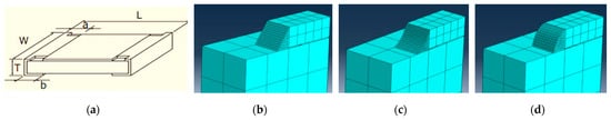
Figure 1.
ERJ-H3G Resistor component specification [8] (panel (a)); FE models for straight, concave, and convex geometries (panels (b), (c), and (d), respectively).
Course hexahedral mesh is used for the PCB and the chip resistor, as shown in panels b, c, and d of Figure 1. Because the solder joint is the critical region, fine mesh is set up for it. However, due to the uneven geometry, tetrahedral elements are used here. The total number of nodes are 963, 934, and 987 for the straight, concave, and convex models, respectively.
2.2. Material Properties
The exposure of electronic devices to fluctuating thermal conditions leads to material degradations such as creep and fatigue, which often culminate in failure. Solder joints experience creep due to sustained stress, especially at elevated temperatures. The modeling of viscoplastic behavior is crucial when estimating fatigue lifetime. Therefore, the Anand material model was applied for the solder joint. The Anand parameters of the SAC305 material were taken from [5]. All other material parameters are collected in Table 1.

Table 1.
Material properties (Definition of abbreviations: E—Young’s modulus, ν—Poisson’s ratio, CTE—Coefficient of Thermal Expansion).
2.3. Thermal Cycle Parameters
The temperature cycling properties collected in Table 2 are based on existing standards. Two thermal shock cycles (Types I and II) which are commonly used in reliability testing to assess the durability of solder joints and electronic assemblies are chosen. These usually consist of a 10–15-min dwell time tD and a rapid, less-than-30-second ramp time tR. The other three cycles (Types III, IV, and V) are conventional thermal cycles which are suitable for simulating real-life scenarios where temperature changes occur over time. The thermal cycles were imposed using temperature field definitions over time. The temperature history was controlled using amplitude curves which define how the temperature changes with time across specific steps or intervals between the maximum Tmax and minimum Tmin temperature. These temperature variations resemble realistic operating or environmental conditions where the assembly experiences periodic heating and cooling.
Table 2.
Thermal cycling conditions.
Initially, room temperature Troom = 18 °C was set on the entire model. Troom represents the system’s baseline state before any thermal loading is applied; this ensures that all components—resistor body, solder joints, and substrate—begin from a uniform thermal condition. After ramping up from Troom, four complete cycles were accomplished (see Figure 2).
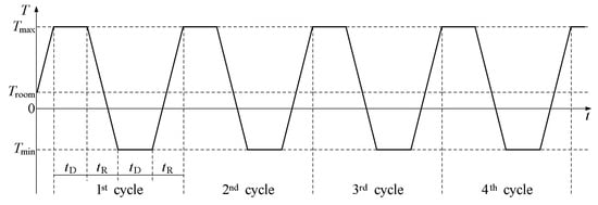
Figure 2.
Thermal cycling pattern.
By prescribing the thermal loading in the above explained manner—through time-dependent temperature fields rather than direct heat flux—the model captures the thermomechanical strain generated by differences in the CTE among the materials. This is essential for evaluating thermal fatigue behavior, as the induced expansion and contraction in the solder joints drive stress accumulation and potential crack initiation over multiple thermal cycles.
2.4. Damage Indicators CEEQ and CENER
The equivalent creep strain (CEEQ) and creep dissipation energy density (CENER) values were evaluated in Abaqus in the post-process phase of the FE simulations. These damage accumulation indicators were calculated by integrating corresponding strain and stress values over time in the four thermal cycles.
CEEQ is generally used to represent the accumulated total creep deformation over time. It shows how much the material has permanently deformed due to long-term loading. Because the solder expands and contracts during the cycles, this can lead to a build-up of creep strain in the material. Over many cycles, this creep strain can build up to a point where micro-cracks are formulated in the solder.
CENER represents the amount of energy per unit volume that is irreversibly dissipated as heat due to creep deformation over time. When a material undergoes creep, internal friction and microstructural changes convert certain portions of the mechanical work into thermal energy. This value helps quantify damage accumulation in regions undergoing creep. In FE analysis of solders, CENER is often used alongside CEEQ to identify critical failure zones. High CENER values typically correlate with areas at risk of crack initiation or fatigue.
2.5. Solder Joint Lifetime Estimation
Three models, the Akay, Syed, and Darveaux models [4], were applied for estimating the lifetime of the solder joint with different geometries and loads. These three models use CEEQ and CENER as input. The Akay model is a creep-damage-based model [9], expressed as follows:
where = Vsolder CENERav is the total strain energy. Material constants are k = −0.8165 = 0.358 Nmm.
Another creep-damage-based model used here is the Syed model [10], expressed as follows:
where = CEEQav is the accumulated creep strain and C = 0.9 is the creep ductility.
The Darveaux model is a damage-accumulation-based model [11] that operates with the crack growth rate and calculates the cycle number until the crack reaches the defined final crack length a in the solder joint. The estimated lifetime in cycles is as follows:
where = CENERav, which is the average viscoplastic strain energy density; empirical constants are = 14, = −0.9, = 0.014, and = 0.7; and the final crack length a = 0.55 mm.
3. Results
3.1. Damage Indicators CEEQ and CENER
Figure 3 and Figure 4 show the FE results on CEEQ and CENER for the thermal shock cycle Type I and the conventional thermal cycle Type III. In both Figure 3 and Figure 4, CEEQ is shown in the top row, while CENER is in the bottom row. The first, second, and third columns contain the results for the straight, concave, and convex geometries, respectively. The color scale goes from 0 to 0.25 for CEEQ (dimensionless) and from 0 to 13 mJ/mm3 for CENER. The corresponding numerical data are illustrated by the graphs in Figure 5.
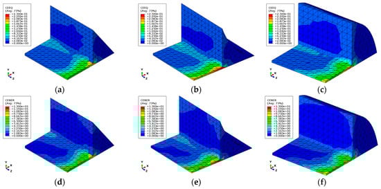
Figure 3.
Thermal shock cycle Type I: CEEQ results for straight, concave, and convex geometries, respectively, in panels (a–c); CENER results for straight, concave, and convex geometries, respectively, in panels (d–f).
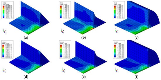
Figure 4.
Thermal cycle Type III: CEEQ results for straight, concave, and convex geometries, respectively, in panels (a–c); CENER results for straight, concave, and convex geometries, respectively, in panels (d–f).
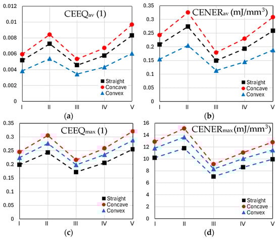
Figure 5.
Test matrices with CEEQ (1) and CENER (mJ/mm3) results: cycle Types I, II, III, IV, and V in the horizontal axes; geometry types indicated by different markers: (a) average CEEQ values (b) average CENER values (c) maximum CEEQ values (d) maximum CENER values.
3.2. Thermal Fatigue Lifetime Estimations
The fatigue lifetime of the solder joints was estimated based on the formulae overviewed in Section 2.5. The resulting lifetime values for the complete test matrix are illustrated in Figure 6.
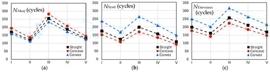
Figure 6.
Test matrices with lifetime (cycles) results: cycle Types I, II, III, IV, and V in the horizontal axes; geometry types indicated by different markers: (a) presents the predicted lifetimes from Akay model, (b) the lifetimes from the fatigue model of Syed and (c) predicted lifetimes from Darveaux.
4. Discussion
4.1. Effect of Geometry on CEEQ and CENER
It can be observed in both Figure 3 and Figure 4 that in all cases, peak CEEQ and CENER and, therefore, the highest probability of micro-crack formation took place on the outer side of the mounting surface. This supports the idea that there is a chance to detect and observe crack initiation and failure by relying on optical techniques in practice.
The highest maximum and average CEEQ and CENER values were registered in the case of the concave solder geometry, as Figure 4 shows. This fact indicates that the concave solder geometry is exposed to the greatest damage accumulation, most probably because it contains the smallest amount of solder material.
The lowest average values appear in the case of the convex solder geometry. Contrarily, the lowest peak (i.e., maximum) CEEQ and CENER values are obtained from the straight geometry. This contradiction indicates that, in terms of CEEQ and CENER, it is not clear whether a straight or convex solder geometry is optimal from the point of view of damage accumulation. The average CEEQ and CENER results indicate that solder volume is a factor of significant importance in lifetime. In terms of maximum CEEQ and CENER, however, straight geometry led to the smallest values. It indicating that it had the best strain distribution out of the three geometry types.
4.2. Effect of Thermal Cycling Profile on CEEQ and CENER Values
The results in Figure 5 indicate a significant increase in CEEQ and CENER under thermal shock (thermal cycle Types I and II), as compared to loadings under conventional thermal cycling profiles (Types II, IV, and V). The finding that a higher temperature gradient leads to greater damage accumulation is in line with the literature [4,5,6].
Not only the timing, but also the temperature range (see Table 2) has a strong effect on damage accumulation. Larger temperature ranges consistently lead to higher values of CEEQ and CENER damage accumulation indicators.
4.3. Interplay of Geometry, Thermal Cycling Properties, and Lifetime
By comparing Figure 5 and 6, one concludes that, in terms of temperature cycling properties, all lifetime models are coherent: higher values of damage accumulation indicators (CEEQ and CENER) lead to lower predicted lifetimes, and vice versa.
However, in terms of solder geometry, there is a contradiction between the Akay model and the two other fatigue lifetime models. The lifetime NSyed produced by the Syed model and the lifetime NDarveaux produced by the Darveaux model (i.e., the number of cycles until 50% probability of failure [4]) are consistent with the average values of CEEQ and CENER, respectively, indicating that larger volume leads to longer lifetime. However, the Akay model suggests that the trend of the lifetime NAkay is inverse to the trend of the solder volume Vsolder. Predicted lifetime is coherent with the average CENER value. However, the longest lifetime results for the concave geometry type, which contains the lowest volume of solder material. This discrepancy occurs because the Akay model accounts for the dissipated energy in the complete solder volume, thereby penalizing larger volumes. This issue has been already observed and explained in [7].
The FE analysis-based virtual test matrix provides insight into the coupled effect of thermal cycling conditions and geometric deviations. Until it is clear whether the Akay model or the other two models are more reliable, the application of straight solder geometry seems the safest choice in virtual lifetime prediction. Also, one can conclude that the Darveaux model with the convex geometry provides the most economic design for any thermal cycling properties because it predicted the highest lifetime among the investigated models while the Syed model with the concave geometry type produced the most conservative lifetime estimation. In light of this information, the contradiction with regard to the Akay model becomes irrelevant in practice.
5. Conclusions
The thermomechanical behavior of chip resistor solder joints under various thermal cycling conditions and various geometries were assessed using FE modeling with a viscoplastic material model. The comparative analysis captured the effect of the temperature cycling intensity—the predicted lifetime significantly reduced under thermal shock. As a new contribution of the work, as well as the thermal cycling parameters, the geometry was also varied. Among the three tested geometries—straight, concave, and convex—the convex configuration demonstrated superior fatigue resistance based on the Syed and Darveaux models, while the concave shape showed higher lifetime using the Akay model. This contradiction arises because the Akay model takes the total volume of the solder and the total dissipated energy into account, thus penalizing larger volume. The contradictions in lifetime predictions highlighted the necessity of model calibration and validation through experimental data.
The Darveaux model with convex geometry yields the most economical design across thermal cycling conditions by predicting the highest lifetime, while the Syed model with concave geometry gives the most conservative estimate for surface-mounted thick-film resistors. Thus, the contradictions with the Akay model become irrelevant in practical applications.
In future work, FE simulations will be conducted with further detailed parametrization of the thermal cycles. The simulation data will be benchmarked with experimentally collected lifetime data.
Author Contributions
Three-dimensional modeling and paper editing, Y.D.; finite element simulations and paper editing, N.K.; finite element simulations, M.J.S., research of background literature, D.S.; evaluation of results, M.M.D.F.; conceptualization and supervision of the work. A.B. All authors have read and agreed to the published version of the manuscript.
Funding
The publication was created in the framework of the Széchenyi István University’s VHFO/416/2023-EM_SZERZ project entitled “Preparation of digital and self-driving environmental infrastructure developments and related research to reduce carbon emissions and environmental impact” (Green Traffic Cloud).
Institutional Review Board Statement
This study did not require ethical approval as it did not involve humans or animals.
Informed Consent Statement
Not applicable, as the study did not involve human participants.
Data Availability Statement
Data supporting the findings of this study are contained within the article.
Acknowledgments
This work was supported by Audi Hungaria Zrt., Győr, Hungary. Special thanks to Tamás Fülöp for the discussions.
Conflicts of Interest
The authors declare no conflicts of interest related to this study.
References
- Yuan, C.; Su, Q.; Chiang, K.N. Coefficient Extraction of SAC305 Solder Constitutive Equations Using Equation-Informed Neural Networks. Materials 2023, 16, 4922. [Google Scholar] [CrossRef] [PubMed]
- Pang, J.H.L.; Chong, D.Y.R.; Low, T.H. Thermal cycling analysis of flip-chip solder joint reliability. IEEE Trans. Compon. Packag. Technol. 2001, 24, 705–712. [Google Scholar] [CrossRef]
- Rizvi, M.J.; Lu, H.; Bailey, C.; Bevan, E.; Pountney, N.; Coates, J. Finite element modelling of failures in thick film chip resistor solder joints. In Proceedings of the 5th International Microsystems Packaging Assembly and Circuits Technology Conference, Taipei, Taiwan, 20–22 October 2010; pp. 1–4. [Google Scholar]
- Su, S.; Akkara, F.J.; Thaper, R.; Alkhazali, A.; Hamasha, M.; Hamasha, S. A State-of-the-Art Review of Fatigue Life Prediction Models for Solder Joint. J. Electron. Packag. 2019, 141, 040802. [Google Scholar] [CrossRef]
- Ha, J.; Lai, Y.; Yang, J.; Yin, P.; Park, S. Enhanced solder fatigue life of chip resistor by optimizing solder shape. Microelectron. Reliab. 2023, 145, 114994. [Google Scholar] [CrossRef]
- Depiver, J.A.; Mallik, S.; Amalu, E.H. Thermal fatigue life of ball grid array (BGA) solder joints made from different alloy compositions. Eng. Fail. Anal. 2021, 125, 105447. [Google Scholar] [CrossRef]
- Bakonyi, A.; Fekete, G.; Zelei, A. In Silico Benchmarking of Fatigue Life Estimation Models for Passive SMD Solder Joints Under Thermal Cycling. Appl. Mech. 2024, 5, 877–907. [Google Scholar] [CrossRef]
- Panasonic High Temperature Thick Film Chip Resistor (Automotive Grade). Available online: https://industrial.panasonic.com/cdbs/www-data/pdf/RDQ0000/ast-ind-151033.pdf (accessed on 11 June 2025).
- Akay, H.U.; Paydar, N.H.; Bilgic, A. Fatigue Life Predictions for Thermally Loaded Solder Joints Using a Volume-Weighted Averaging Technique. ASME J. Electron. Packag. 1997, 119, 228–235. [Google Scholar] [CrossRef]
- Syed, A. Predicting Solder Joint Reliability for Thermal, Power, and Bend Cycle Within 25% Accuracy. In Proceedings of the 51st Electronic Components and Technology Conference, Orlando, FL, USA, 29 May–1 June 2001; pp. 255–263. [Google Scholar]
- Darveaux, R. Effect of Simulation Methodology on Solder Joint Crack Growth Correlation. In Proceedings of the Electronic Components and Technology Conference (ECTC), Las Vegas, NV, USA, 21–24 May 2000; pp. 1048–1058. [Google Scholar]


Disclaimer/Publisher’s Note: The statements, opinions and data contained in all publications are solely those of the individual author(s) and contributor(s) and not of MDPI and/or the editor(s). MDPI and/or the editor(s) disclaim responsibility for any injury to people or property resulting from any ideas, methods, instructions or products referred to in the content. |
© 2025 by the authors. Licensee MDPI, Basel, Switzerland. This article is an open access article distributed under the terms and conditions of the Creative Commons Attribution (CC BY) license (https://creativecommons.org/licenses/by/4.0/).