Proceeding Paper

Design of Complementary Metal–Oxide–Semiconductor Encoder/Decoder with Compact Circuit Structure for Booth Multiplier †

Department of Electronic Engineering, National Chin-Yi University of Technology, Taichung 411030, Taiwan
*
Author to whom correspondence should be addressed.
Presented at the 8th Eurasian Conference on Educational Innovation 2025, Bali, Indonesia, 7–9 February 2025.
Eng. Proc. 2025, 103(1), 21; https://doi.org/10.3390/engproc2025103021
Published: 1 September 2025

Abstract

Multipliers are crucial components in digital processing and the arithmetic logic unit (ALU) of central processing unit (CPU) design. As the data bit length increases, the number of partial products in the multiplication process increases, resulting in an increased summation time for the partial products. Consequently, the speed of the multiplier circuit is adversely affected by increased time delays. In this article, we present a combined radix-4 Booth encoding module that employs metal–oxide–semiconductor (MOS) transistors that share common control signals to reduce the transistor count. In HSPICE simulations, the functionality of the proposed circuit architecture was verified, and the number of transistors used was successfully reduced.

1. Introduction

Multiplication is a fundamental arithmetic operation and is critical in various microprocessors and digital signal processing systems. The traditional multiplication process consists of two main operations: partial product generation and the addition of these partial products. In the digital multiplication of two binary numbers, the multiplicand and the multiplier are used to generate the related partial products. Once all partial products are generated, a matrix of partial products is formed. After this process, related partial products are added, from the least significant bit (LSB) to the most significant bit (MSB), by using a digital adder array. In a multiplier chip design, the adder array used for partial product accumulation is a major source of the chip area, time delay, and power consumption. Furthermore, as the data bit length increases, the traditional adder array needs more time to calculate the corresponding sum and carry values. The operating time of a multiplier in a traditional circuit architecture increases with the bit length of input data.
Booth’s multiplication algorithm was invented in the 1950s by Andrew Donald Booth, a British electrical engineer and computer scientist. Radix-4 Booth encoding technology reduces the number of partial product rows but effectively decreases the number of accumulation operations. As a result, the overall performance of multipliers is improved by Booth encoding, compared with that of the conventional multiplier circuits. By encoding the input data of the multiplier, the number of partial product rows is decreased. The reduction in partial product rows means that fewer adders are required. Fewer adders lead to significant reductions in the multiplier’s area, delay, and power consumption [1,2]. Therefore, the technique of radix-4 Booth encoding is often employed in advanced multiplier designs [3,4,5,6,7].
In this study, we explored the design of the corresponding complementary metal–oxide–semiconductor (CMOS) circuit for the radix-4 Booth encoder/decoder. Furthermore, we simplified the circuit design and reduced power consumption at the cost of a slight time delay penalty.

2. Radix-4 Booth Encoding

The Booth algorithm, first proposed by Andrew D. Booth in 1951 [8], is based on the data of the multiplier. If consecutive 1s in the multiplier are detected, the bits starting from the first 1 in the sequence are changed to a value of −1, with the next bit after the consecutive 1s being set to 1, while the bits in between are set to 0. Therefore, as the number of 0s in the multiplier increases, the number of generated partial product rows that require addition operations decreases as follows:
( 14 ) 10   =   ( 0   0   1   1   1   0 ) 2
X   ×     0   0   1   1   1   0   2 = X   ×     2 3 + 2 2 + 2 1 = X   ×   14
X   ×   ( 0   1   0   0 1   0 ) 2   = X   ×   2 4 2 1 = X   ×   14  
where X is the multiplicand, and the number 14 in this case is the multiplier. Equation (1) shows the binary representation of the decimal number 14. In traditional multiplication, as shown in Equation (2), three partial products are generated. However, if we convert from (0 0 1 1 1 0)2 to (0 1 0 0 −1 0)2, (3), only two partial products are generated in this case.
The traditional Booth encoding, specifically referred to as radix-2 Booth encoding, was proposed in Ref. [8]. The encoding method is shown in (6), and this method does not reduce the number of products generated. Therefore, this encoding is not effective in reducing the generation of partial product rows.
B 10 = i = 0 n 1 b i × 2 i
( B ) 10 = b n 1 × 2 n 1 + i = 0 n 2 b i × 2 i
B = b n 2 b n 1 × 2 n 1 + b n 3 b n 2 × 2 n 2 + b n 4 b n 3 × 2 n 3 + + b 0 b 1 × 2 1 + b 1 b 0 × 2 0
Radix-4 Booth encoding [1] is an improvement over radix-2 Booth encoding and is also called modified Booth encoding. Its encoding method, as shown in (7), reduces the number of partial product rows from n to either n/2 or (n/2) + 1, depending on whether the multiplication is signed or unsigned. The coefficients for radix-4 Booth encoding, with a digit set of −2, −1, 0, 1, and 2, are shown in Table 1, where Y represents the multiplier, X represents the multiplicand, and PP represents the coefficient of the partial product.
B = 2 b n 1 + b n 2 + b n 3 × 2 n 2 + 2 b n 3 + b n 4 + b n 5 × 2 n 4 + + 2 b 3 + b 2 + b 1 × 2 2 + 2 b 1 + b 0 + b 1 × 2 0

3. Proposed Radix-4 Booth Encoding Module

3.1. Encoder

The radix-4 Booth coding module is illustrated in Figure 1a, with its generated coefficients presented in Table 2. The signal negi represents a negative multiplier and is directly generated by the signal Y2i+1. The signal YiS represents a multiple of 1 and is generated by a CMOS-based XOR gate, with its inverted signal YiSI produced through an inverter. The signal YiC represents a multiple of 2 and is generated by a 3-3 OAI (OR-AND-Invert) structure, with its inverted signal YiCI also produced through an inverter. The signal zeroi represents a multiple of 0 and is generated by a 3-3 OAI (OR-AND-Invert) structure. The signal Si is a correction bit required for the modified sign extension structure technique proposed in reference [9], considering its use in the adder array. The signal Si is generated by a 2-1 AOI (AND-OR-Invert) structure, with its inverted signal SiI produced through an inverter.

3.2. Decoder

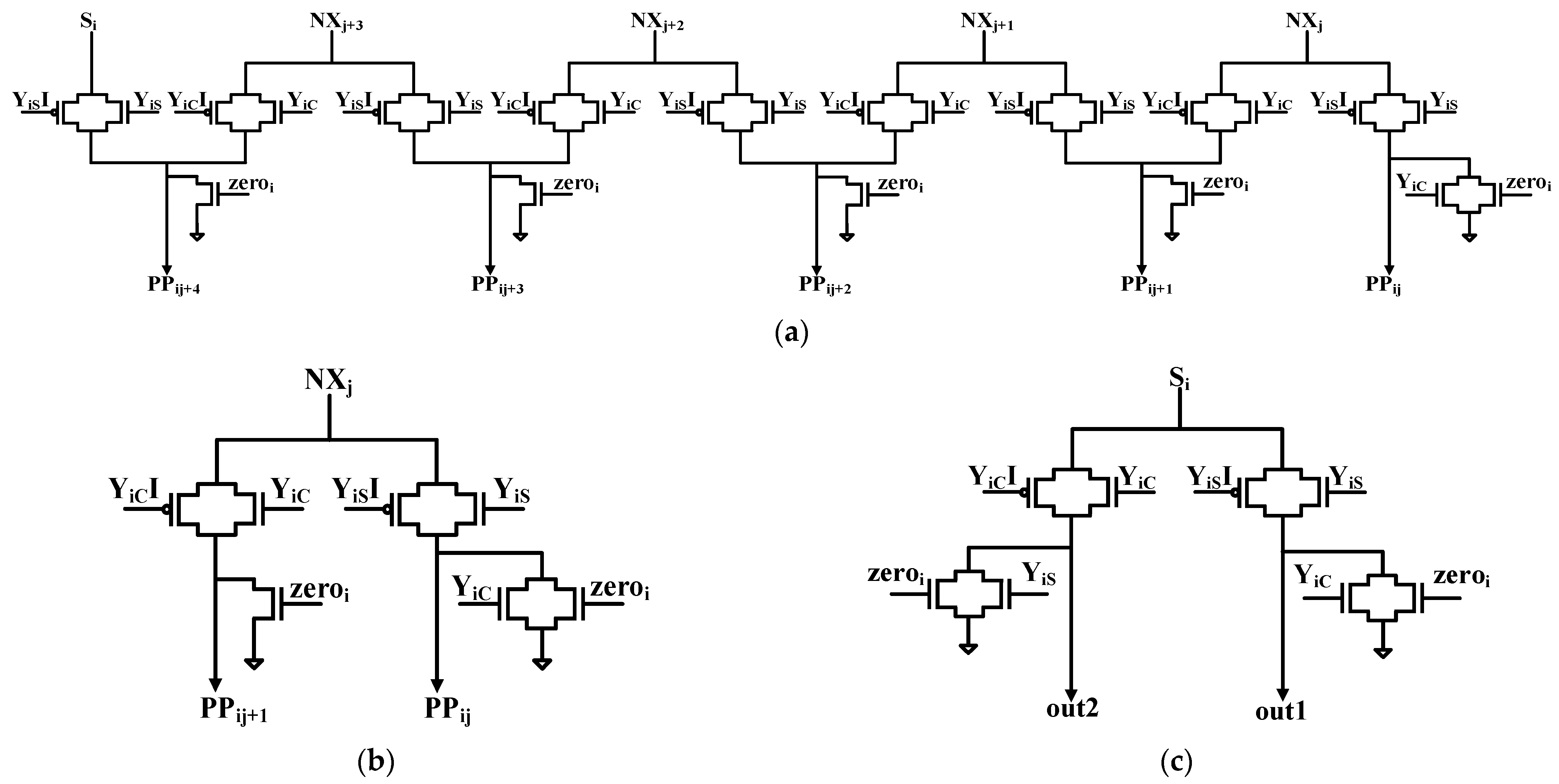
The transistor-level implementation of the demux-type 4-bit radix-4 Booth decoder circuit is illustrated in Figure 2a. Each stage of the demux is controlled by a transmission gate (TG), which is driven by the YiS and YiC signals. The first stage of the decoder circuit is illustrated in Figure 2b, which demonstrates the elemental principles. By observing the signals YiS, YiC, and zeroi in Table 2, signals YiS, YiC, and zeroi never become 1 simultaneously. When signal YiS = 1, the TG gate controlled by signal YiS is turned on, while the TG gate controlled by signal YiC remains off, and the signals NXj output is directed to PPij. When signal YiC = 1, the TG gate controlled by signal YiS remains off, while the TG gate controlled by signal YiC and the NMOS connected to PPij turn on. The signals NXj output is directed to PPij+1, and the NMOS outputs 0 to PPij. When signals zeroi = 1, both TG gates remain off, and the NMOS controlled by the signal zeroi turns on, outputting 0 to all PP. The demux-type decoder used to output the correction bit Si is illustrated in Figure 2c. Its operation is the same, with the difference being the additional NMOS controlled by the signal YiS at out2. When the signal YiS = 1, the NMOS conducts and outputs 0 to out2.

4. Circuit Improvement and Simulation Results

4.1. OAI_zeroi and OAIT_zeroi

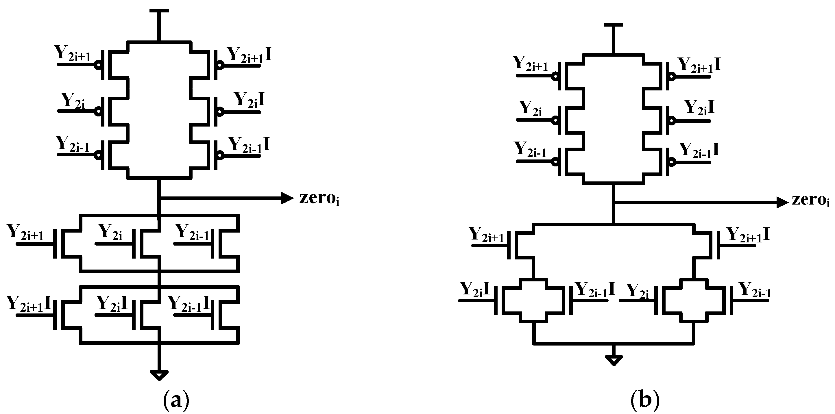
The OAI structure used to generate the signal zeroi is illustrated in Figure 3a. Its delay time was imbalanced, so the NMOS part was modified, resulting in the architecture illustrated in Figure 3b. Compared with the original structure, the delay time of the proposed architecture is more balanced, with values closer to those of the original structure’s better performance, as shown in Table 3.

4.2. Xj_2 and Xj2

In the decoder, the signal NXj is obtained by performing an XOR operation between the multiplicand Xj and the signal Y2i+1, indicating a negative value in Booth encoding. The operation results are shown in Table 4. When Y2i+1 = 0, it indicates a positive value, and the signal NXj is the same as Xj. Conversely, when Y2i+1 = 1, it indicates a negative value, and the signal NXj is the inverse of Xj. The corresponding truth table is shown in Table 4.
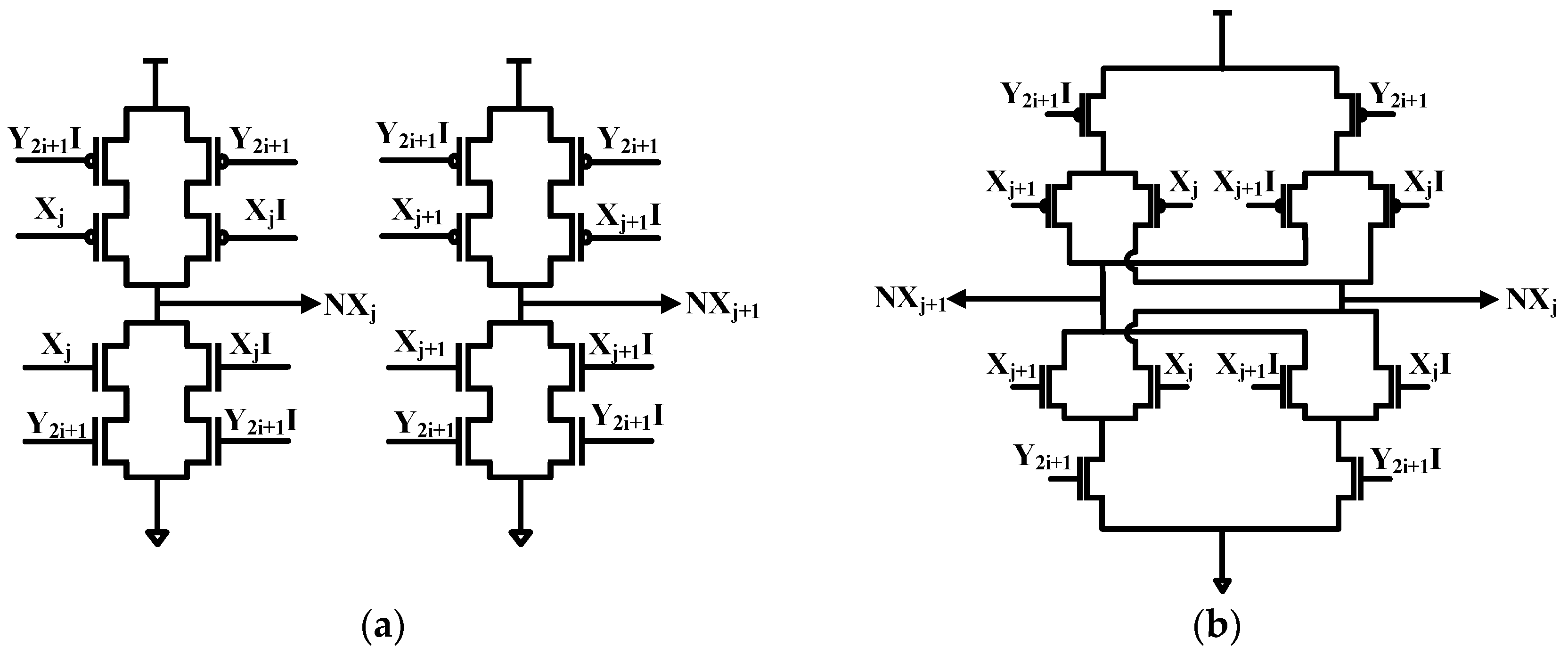
Figure 4a illustrates two CMOS-type XOR gates, which share the signal Y2i+1 from the same Booth encoding group. To optimize the design, they were merged into a single structure by sharing MOS transistors controlled by the common signal, resulting in the architecture shown in Figure 4b. Table 5 presents a comparison of the original and revised architectures, showcasing the proposed design’s advantages in terms of reduced power consumption, lower delay, and a reduced number of transistors.

4.3. z_c_s, zc_s, and zcs

The original architecture for generating the Booth encoding signals YiC, YiS, and zeroi is illustrated in Figure 5a. In this design, many MOS transistors are controlled by the same signals. To optimize the design, we implemented a shared MOS approach. The combined architecture for generating the zeroi and YiC signals is shown in Figure 5b, while Figure 5c presents the fully integrated architecture, which also incorporates YiS signal generation. Table 6 provides a comparison of these three architectures. Although the fully merged design reduces the transistor count compared to the other two, it exhibits greater signal delay.

5. Conclusions

We examined a circuit design for shared MOS transistors to reduce the transistor count. By sharing MOS transistors controlled by the same signals, different signal generation architectures are merged into a single design. The proposed architecture in this study maintains correct functionality. Although it does not yield significant improvements in power consumption or delay time, it successfully reduces the number of transistors used.

Author Contributions

Conceptualization, Y.-N.W. and Y.-C.H.; experiments and data validation, Y.-N.W.; writing—original draft preparation, Y.-N.W.; writing—review and editing, Y.-C.H. All authors have read and agreed to the published version of the manuscript.

Funding

This research received no external funding.

Institutional Review Board Statement

Not applicable.

Informed Consent Statement

Not applicable.

Data Availability Statement

All simulated results were obtained by using HSPICE simulator of EDA (electronic design automation) software tools for VLSI designing.

Acknowledgments

We would like to express our gratitude to the United Microelectronics Corporation (UMC), Taiwan, and the Taiwan Semiconductor Research Institute (TSRI) for providing the EDA software that allows us to perform IC layout and simulations at our laboratory.

Conflicts of Interest

The authors declare no conflicts of interest.

References

  1. MacSorley, O. High-speed arithmetic in binary computers. IRE Proc. 2007, 49, 67–91. [Google Scholar] [CrossRef]
  2. Rubinfield, L.P. A proof of the modified Booth’s algorithm for multiplication. IEEE Trans. Comput. 1975, 24, 1014–1015. [Google Scholar] [CrossRef]
  3. Cheng, Q.; Dai, L.; Huang, M.; Shen, A.; Mao, W.; Hashimoto, M.; Yu, H. A low-power sparse convolutional neural network accelerator with pre-encoding radix-4 Booth multiplier. IEEE Trans. Circuits Syst. II: Express Briefs. 2023, 70, 2246–2250. [Google Scholar] [CrossRef]
  4. Wang, H.; Liu, Y.; Han, J. The design of multipliers based on radix-4 Booth coding. In Proceedings of the 2022 4th International Academic Exchange Conference on Science and Technology Innovation (IAECST), Guangzhou, China, 9–11 December 2022; pp. 1471–1475. [Google Scholar]
  5. Cui, X.; Liu, W.; Chen, X.; Swartzlander, E.E.; Lombardi, F. A modified partial product generator for redundant binary multipliers. IEEE Trans. Comput. 2016, 65, 1165–1171. [Google Scholar] [CrossRef]
  6. Park, J.; Kim, S.; Lee, Y.-S. A low-power booth multiplier using novel data partition method. In Proceedings of the 2004 IEEE Asia-Pacific Conference on Advanced System Integrated Circuits, Fukuoka, Japan, 4–5 August 2004; pp. 54–57. [Google Scholar]
  7. Abu-Khater, I.S.; Bellaouar, A.; Elmasry, M.I. Circuit techniques for CMOS low-power high-performance multipliers. IEEE J. Solid-State Circuits. 1996, 31, 1535–1546. [Google Scholar] [CrossRef]
  8. Booth, A.D. A signed binary multiplication technique. Quart. J. Mech. Appl. Math. 1951, 4, 236–240. [Google Scholar] [CrossRef]
  9. Ercegovac, M.D.; Lang, T. Digital Arithmetic; Morgan Kaufmann: Los Altos, CA, USA, 2003. [Google Scholar]
Figure 1. (a) The gate-level encoder for the signals negi, YiC, YiS, zeroi, and Si generator; (b) the transistor-level encoder for the YiS generator; (c) the transistor-level encoder for the YiC generator; (d) the transistor-level encoder for the Si generator.
Engproc 103 00021 g001
Figure 2. (a) The transistor-level implementation of the demux-type 4-bit radix-4 Booth decoder circuit; (b) the first stage of the decoder circuit; (c) the demux-type decoder used to output the correction bit Si.
Engproc 103 00021 g002
Figure 3. (a) OAI_zeroi; (b) OAIT_zeroi.
Engproc 103 00021 g003
Figure 4. (a) Xj_2; (b) Xj2.
Engproc 103 00021 g004
Figure 5. (a) z_c_s; (b) zc_s; (c) zcs.
Engproc 103 00021 g005
Table 1. Coefficients of radix-4 Booth encoding.
Y2i+1Y2iY2i−1PP Coef. 1
000 0   ×  Xj
001 + 1   ×  Xj
010 + 1   ×  Xj
011 + 2   ×  Xj
100 2   ×  Xj
101 1   ×  Xj
110 1   ×  Xj
111 0   ×  Xj
1 Coefficient of the partial product.
Table 2. Coefficients of the radix-4 Booth encoding module.
Y2i+1Y2iY2i−1PP Coef.negiYiCYiSzeroiSi
000 0   ×  Xj00010
001 + 1   ×  Xj00100
010 + 1 ×  Xj00100
011 + 2   ×  Xj01000
100 2   ×  Xj11001
101 1   ×  Xj10101
110 1   ×  Xj10101
111 0   ×  Xj10010
Table 3. Simulation results of OAI_zeroi and OAIT_zeroi.
OAI_zeroiOAIT_zeroi
Avg. (uW)9.29579.4973
Delay (ps)80.8/12091.1/86.4
Table 4. Truth table of the signals NXj and NXj+1 generator.
Y2i+1Xj+1XjNXj+1NXj
00000
00101
01010
01111
10011
10110
11001
11100
Table 5. Simulation results of Xj_2 and Xj2.
Xj_2Xj2
Avg. (uW)12.144310.9709
Delay Time (ps)NXj 66.4/32.7NXj 60.7/28.4
NXj+1 66.3/32.8NXj+1 45.2/39.2
Numbers of Transistors11 PMOS9 PMOS
11 NMOS9 NMOS
Table 6. Simulation results of z_c_s, zc_s, and zcs.
z_c_s
(Figure 5a)
zc_s
(Figure 5b)
zcs
(Figure 5c)
Avg. (uW) 23.882723.081423.2156
Delay Time (ps)YiC123/117182/116164/127
YiCI141/143199/143180/155
YiS88.5/11579.5/105123/158
YiSI107/14298.8/13195.3/141
zeroi105/86.4102/144113/137
Numbers of Transistors 23 PMOS19 PMOS17 PMOS
23 NMOS19 NMOS17 NMOS
Disclaimer/Publisher’s Note: The statements, opinions and data contained in all publications are solely those of the individual author(s) and contributor(s) and not of MDPI and/or the editor(s). MDPI and/or the editor(s) disclaim responsibility for any injury to people or property resulting from any ideas, methods, instructions or products referred to in the content.