1. Introduction
The measurement of complex dielectric properties, namely relative permittivity (
) and loss tangent (
), holds increasing significance across diverse applications ranging from communication devices to military systems. Material characterization is a crucial aspect of the design of microwave RF and electronic devices, in which electrical, thermal, and mechanical properties influence the overall behavior of the circuit [
1]. A comprehensive understanding of the properties of materials operating at microwave frequencies is imperative. Challenges arise due to discrepancies in the measured values of the dielectric constant
, which can result from the use of different test methods—such as Full Sheet Resonance (FSR) and X-band clamped stripline resonators—and variations in the interactions of electromagnetic (EM) fields with the substrate. These factors can lead to results differing in unexpected ways between target applications and testing conditions [
2].
In microwave and millimeter-wave technology, the effectiveness of RF devices critically depends on the quality of modern RF substrates. These substrates must be accurately characterized to ensure reliability and enhance credibility in the competitive RF market. Additionally, RF researchers and engineers require precise electromagnetic (EM) 2D/3D simulations based on accurate real-world data on the dielectric properties of materials, including substrates, low-heights, multi-layer composites, and absorbers, to design efficient and high-performing devices.
Substrate manufacturers employ various methods for material characterization at high frequencies. These methods primarily utilize resonant cavities, including coplanar waveguides [
3,
4], transmission lines [
5], and resonant structures such as the coaxial line [
6,
7]. However, these existing methods often suffer from limitations, including narrow frequency bands, destructive sample preparation, and the difficulty of isolating material properties from conductor effects in transmission lines.
Common methods like those using capacitance meters are unsuitable for high-frequency applications due to the increased parasitic inductance and resistance (RLC effects) that affect test fixtures and probes operating beyond 1 GHz.These parasitic components can introduce significant measurement errors, reducing measurement accuracy in RF applications [
8]. The resonant-cavity method, on the other hand, is highly accurate but operates within narrow frequency bands. The typical frequency range for application of the resonant-cavity method is usually limited to a specific band determined by the resonator’s design. For example, it is often tuned to frequencies such as 10 GHz or 30 GHz or even to higher frequencies depending on the cavity structure and can measure only a limited range within these frequencies [
9]. Additionally, the method is often destructive, meaning the sample may need to be altered or cut to fit inside the cavity, which is a drawback for materials that are sensitive or costly to prepare.
Methods utilizing transmission lines without corrected conductor effects lack precision (with error values up to 10%) for values of relative permittivity and loss tangent, particularly at low frequencies [
10]. Planar transmission lines offer improved permittivity estimation for low-height substrates utilizing either the FSR test method or the Stripline Resonator Method (SRM) [
11]. However, challenges arise because the propagation constant depends on both the dielectric low-height and the metallic conductors in the transmission line, making it difficult to separate the two components. This issue poses challenges in calculating low-height permittivity, rendering these methods inappropriate for characterizing the studied low-k low-height substrates [
12,
13]. Early methods using patch antennas for dielectric characterization were introduced by Du in 1986 [
14]. While these approaches were effective in narrowband setups, they typically relied on a single resonant mode and did not account for fabrication-related nonidealities. Building upon this foundation, our method introduces three key refinements: (1) wideband iterative fitting across multiple resonances; (2) compensation for fringing fields, surface waves, and dimensional variability; and (3) the use of both reflection coefficient and input impedance for dual-parameter convergence.
In a departure from traditional approaches, this study introduces a wideband technique (8–16 GHz) specifically designed to mitigate distortions caused by fringing fields and surface waves. These phenomena, which become particularly critical in RF design when dealing with low-height substrates with thicknesses ≤0.4 mm, can mimic capacitance and lead to significant discrepancies between simulation and measurement data, ultimately affecting circuit performance. Our method, tailored to address these challenges in high-performance RF circuits, offers accurate, adaptable, and cost-efficient characterization. Although it does not eliminate the need for destructive sample preparation, it substantially overcomes most existing limitations.
Microwave and RF designers invest significant time, computational resources, and financial effort into the development of electromagnetic (EM) simulation tools that accurately predict circuit behavior. These tools depend critically on precise modeling of material parameters—particularly the relative permittivity (
) and loss tangent (
)—to ensure alignment between simulated and measured circuit performance [
13,
15]. However, it is not uncommon for discrepancies to arise between simulated responses based on nominal datasheet values and the actual measurements obtained from fabricated devices. To mitigate these mismatches, a tuning phase is often employed. During this phase, dielectric parameters are adjusted in simulation to achieve better agreement with physical results. This challenge becomes even more pronounced when designers are dealing with anisotropic substrates or multilayer stackups [
16].
While manufacturers provide nominal and values, there are multiple practical scenarios in which these values require post-fabrication validation. Examples include the following:
Dispersive materials such as polyimide or PTFE composites used in Ku-band and mm-wave systems, in which dielectric properties vary significantly with frequency.
Non-standard or hybrid stackups (e.g., RO4000/FR-4 laminates) affected by bonding, etching, or thermal processing.
Substrates subjected to environmental aging, humidity, or thermal cycles that lead to material degradation.
Flexible or conformal dielectrics in wearable or curved-surface antennas, in which mechanical stress and boundary effects influence effective properties.
In such cases, relying solely on nominal datasheet values can result in inaccurate frequency predictions, mismatched impedances, or degraded antenna performance. The method proposed in this work provides a systematic route for extracting effective material parameters under these application-specific conditions.
The proposed method is built on resonant patch structures designed for wideband behavior in the 8–16 GHz range. While resonant-based techniques themselves are well-established, our approach enhances their utility through multimode patch antenna design, iterative fitting of both and , and practical calibration using measured data. By refining substrate parameter extraction through retrosimulation, we improve the simulation-to-measurement correlation and reduce the dependency on operator expertise. This is particularly critical for real-world environments where non-idealities such as fringing fields, surface waves, and parasitic radiation are pronounced.
A key insight emerging from our study is that low-height substrates (thickness mm) are highly sensitive to fringing field effects and surface wave propagation, which are often underestimated in classical modeling approaches. These phenomena introduce deviations between expected and actual behavior, leading to design inaccuracies. Through controlled iterative refinement, we demonstrate that dielectric parameters reported in datasheets frequently fail to account for these effects—necessitating re-evaluation for reliable RF and microwave design performance.
To address these discrepancies, we propose a cost-effective method that accounts for the variability in the fabrication process. specifically for its influence on the relative permittivity () and the loss tangent () of low-height substrates. This method can be universally applied across industrial labs, R&D centers, and universities, particularly for the design of antennas on low-height substrates. Our technique involves fabricating a multimode patch antenna and extracting the values and using the measurements of the S-parameter and numerical fitting. This approach not only handles the fringing field effects but also integrates iterative fitting to ensure that the final dielectric values accurately reflect the real-world behavior of the material. To validate this method, these refined values were applied in the design of ~9 GHz monomode antennas, in which application they yielded excellent alignment between measurements and simulations, thus proving the reliability and precision of our method.
The proposed method was applied to three low-height base materials: RO4350B (254.7 μm), RO4450F (202 μm), and RO4003C (203 μm). The design and manufacturing of a random multimode antenna within a wide frequency band (11–19 GHz) were carried out for each material. Measurements performed using a ZNA67 Rohde & Schwarz (Munich, Germany) Vector Network Analyzer (VNA) included the real and imaginary parts of the input impedance, , as well as the reflection coefficient, . Analyzing input impedance, , rather than relying solely on the reflection coefficient, , provides deeper insights into the EM behavior of the materials. Although this technique requires physically cutting the substrate to create different antennas, making it destructive, its strength lies in its ability to handle low-height substrates and account for fringing field effects that cause significant differences between simulated and measured data.
To summarize, our contribution addresses three core challenges in substrate characterization for modern RF design:
Wideband multimode characterization (8–16 GHz): Traditional narrowband techniques (e.g., split-cylinder [
17,
18] and split-post resonator methods [
19,
20]) extract dielectric properties at isolated frequencies. In contrast, our approach leverages multimode antenna behavior across a broad frequency range, enabling multi-resonance fitting for improved accuracy, explicit modeling of fringing fields and surface roughness, and iterative convergence using both
and
.
Cost-effective implementation: The method relies on standard PCB fabrication and commercially available measurement equipment, avoiding the high cost and complexity of systems such as Fabry–Perot interferometers [
21] or open-space setups [
22] and thus making it accessible to both industry and academia.
Efficient algorithmic fitting: A secant-based tuning algorithm allows for fast convergence (typically ≤ 6 iterations), with results that meet strict validation criteria (≤0.2% frequency error, ≤10% MRE for
), improving the reproducibility of parameter extraction across tools [
23,
24].
While resonator-based characterization techniques are well established, our work refines and extends these methods specifically for low-height profile substrates (thickness ≤ 0.4 mm), for which classical assumptions—such as negligible fringing or uniform field confinement—often break down. By integrating wideband multimode behavior, compensation for real-world fabrication effects, and dual-domain simulation fitting (both and ), the proposed workflow delivers a scalable and transferable methodology for accurate dielectric evaluation in practical RF design environments. Importantly, the proposed method is not intended to replace industrial-grade metrology used by substrate manufacturers, who routinely employ narrowband, high-precision cavity or transmission-line techniques. Instead, our approach is designed for RF engineers, system integrators, and academic researchers seeking material validation in specific assembled contexts—such as altered stack-ups, nonstandard dielectrics, or frequency-dispersive substrates. Representative use cases include prototyping with aged or third-party materials, verifying flexible substrates, and re-characterizing laminates in 5G/6G and conformal antenna applications.
This paper is structured as follows:
Section 2 explains the technical details of the characterization method;
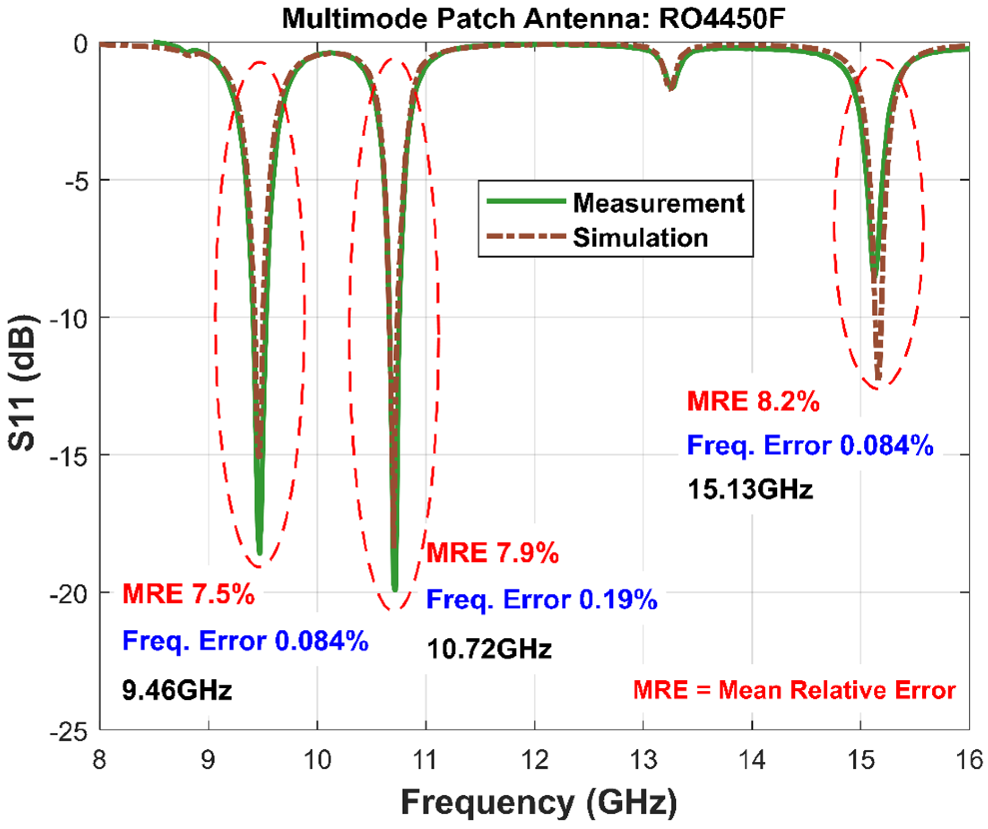
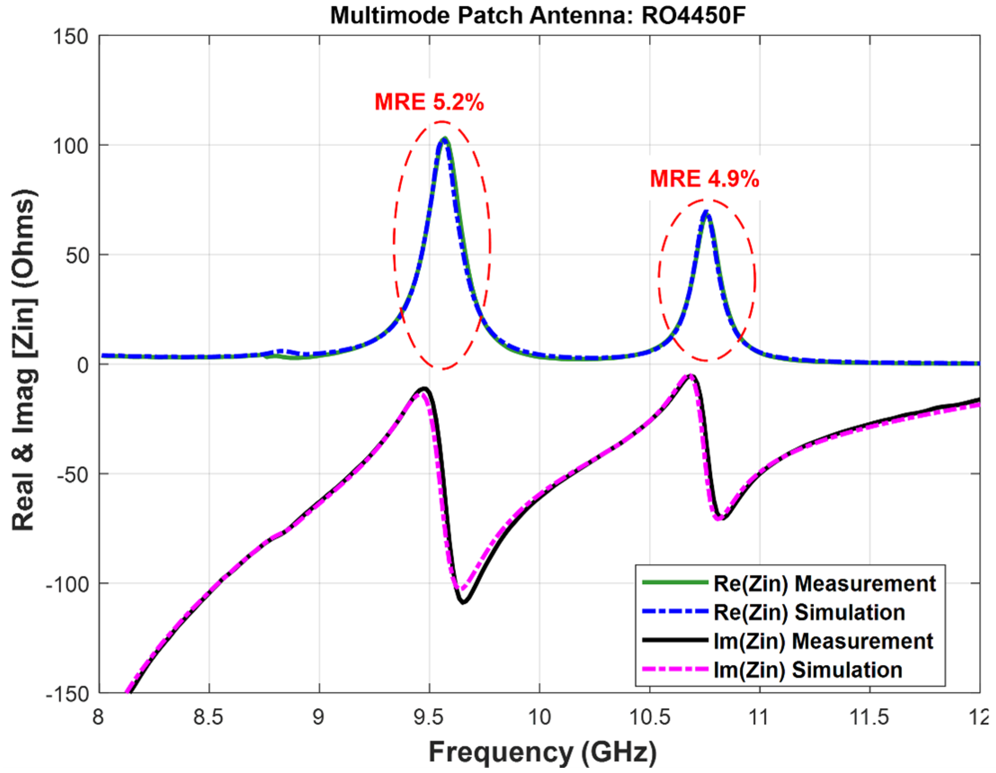
Section 3 presents experimental results for all three substrate materials and the manufactured patch antennas;
Section 4 provides a discussion of the methodological strengths and limitations of the proposed technique; and finally,
Section 5 concludes the work and offers perspectives and directions for future work on the proposed method.
2. The Characterization Method
The properties of dielectric substrate materials often deviate slightly from the manufacturer’s specified data due to variability in the fabrication process. The key parameters for designers of antennas and microwave circuits are the relative dielectric permittivity and the loss tangent . Even minor variations in these parameters can significantly impact circuit performance, leading to issues such as shifts in resonant frequency and impedance mismatches. Consequently, the accurate characterization of substrate materials is an indispensable phase in the design process, as it directly influences the reliability and efficiency of microwave components.
In this study, the characterization method integrates both simulation and experimental measurements and is structured in three sequential steps:
Design, fabrication, and measurement of a multimode patch antenna.
Numerical fitting of the measured results by fine-tuning the substrate parameters (, ).
Design, fabrication, and measurement of a monomode antenna for validation purposes.
The steps involved in the proposed characterization method are detailed in
Figure 1.
A multimode antenna is chosen in Step 1 to increase the statistical accuracy of the characterization process. These antennas exhibit multiple resonant frequencies (“spikes”) within a wideband frequency range, a behavior that can provide more data points for fitting during retrosimulation. This abundance of spikes helps reduce the error probability, as more resonances allow for a better match between simulations and measurements, statistically lowering the fitting error margin. The use of multimode antennas not only enhances data density but also helps in identifying potential anomalies in the properties of the dielectric material.
In Step 3, a monomode antenna is used to validate the fitted parameters. These antennas have a single resonance point at 9 GHz, making it harder to directly fit the substrate parameters. However, if the obtained relative permittivity and loss tangent values were to accurately predict the performance of a monomode antenna (one having a single resonant frequency), such a result would strongly confirm the validity of the method. This validation is crucial because it reinforces the integrity of the initial assumptions regarding the substrate materials, ensuring that the characterization process is not just an isolated exercise, but is linked to practical applications. Essentially, a successful fit of the retrosimulated values to a monomode antenna demonstrates that the technique effectively characterizes the substrate, validating the accuracy of the entire process.
2.1. Step 1: Design of the Multimode Antenna
The initial phase involves designing and fabricating a multimode patch antenna adapted to the targeted characterization frequency, which is typically within the range of 8 to 16 GHz. The design process uses advanced EM-simulation tools to fine-tune critical parameters such as patch dimensions and feed mechanisms, which are essential for optimal bandwidth and efficiency. The antenna’s design includes specific dimensions and shapes to support multiple resonant peaks. The inclusion of a greater number of these peaks is crucial, not arbitrary, as it enhances frequency diversity and allows for better characterization of substrate materials in a wide permittivity range.
Subsequently, discrepancies arise between the
and
measured via VNA and the simulated results, highlighting the impact of manufacturing variability on the substrate’s parameters. These variations can be categorized as deterministic errors (systematic deviations due to fabrication tolerances) or stochastic errors (random variations influenced by environmental factors). The impact of these variations is taken into account in the theory of the resonant cavity model applied to the analysis of patch antennas.
Figure 2 demonstrates that the relative permittivity
influences the resonant frequency
for all modes, as described by Equation (
1). This equation serves as a conceptual expression derived from the rectangular cavity resonator model, illustrating the dependence of the resonant frequency
on the effective permittivity
. It is not used directly in our extraction process but rather provides intuition regarding the modal frequency shifts observed in multimode patch antennas. It can be written as follows:
where
L,
W, and
h represent the geometric length and width of the patch antenna’s top conductor and the substrate’s thickness (i.e., height). Additionally, the loss tangent
primarily influences the depth of the reflection coefficient minimum near resonance. Higher values of
increase dielectric losses, which reduce the sharpness of the
curve and the peak of the input impedance response. While
does not alter the resonant frequency itself, it plays a significant role in determining the quality and amplitude of the impedance match.
The actual values of and are determined using full-wave 3D electromagnetic simulations (CST Microwave Studio and ADS FEM), which are calibrated against measured and responses of the fabricated antenna.
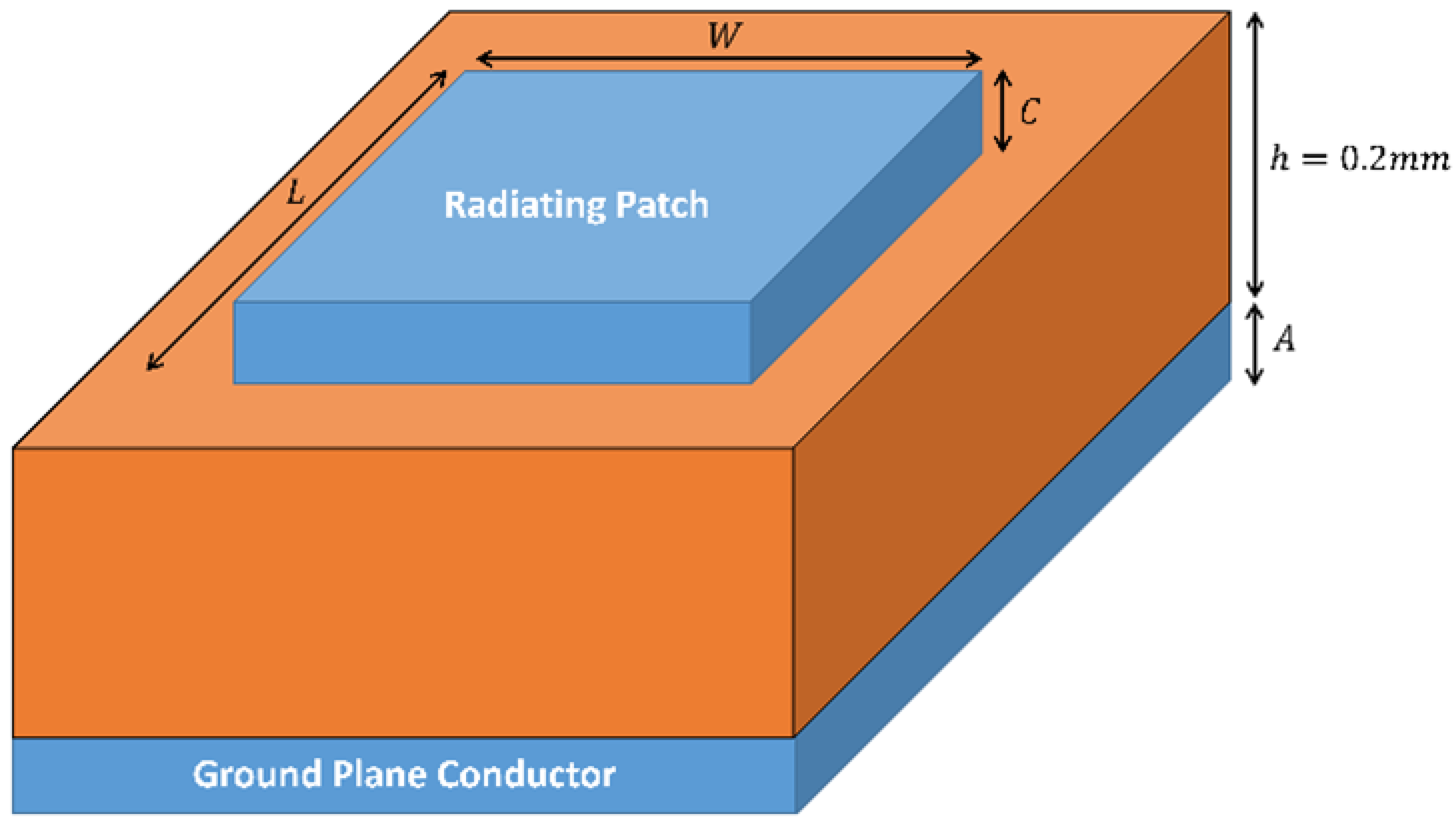
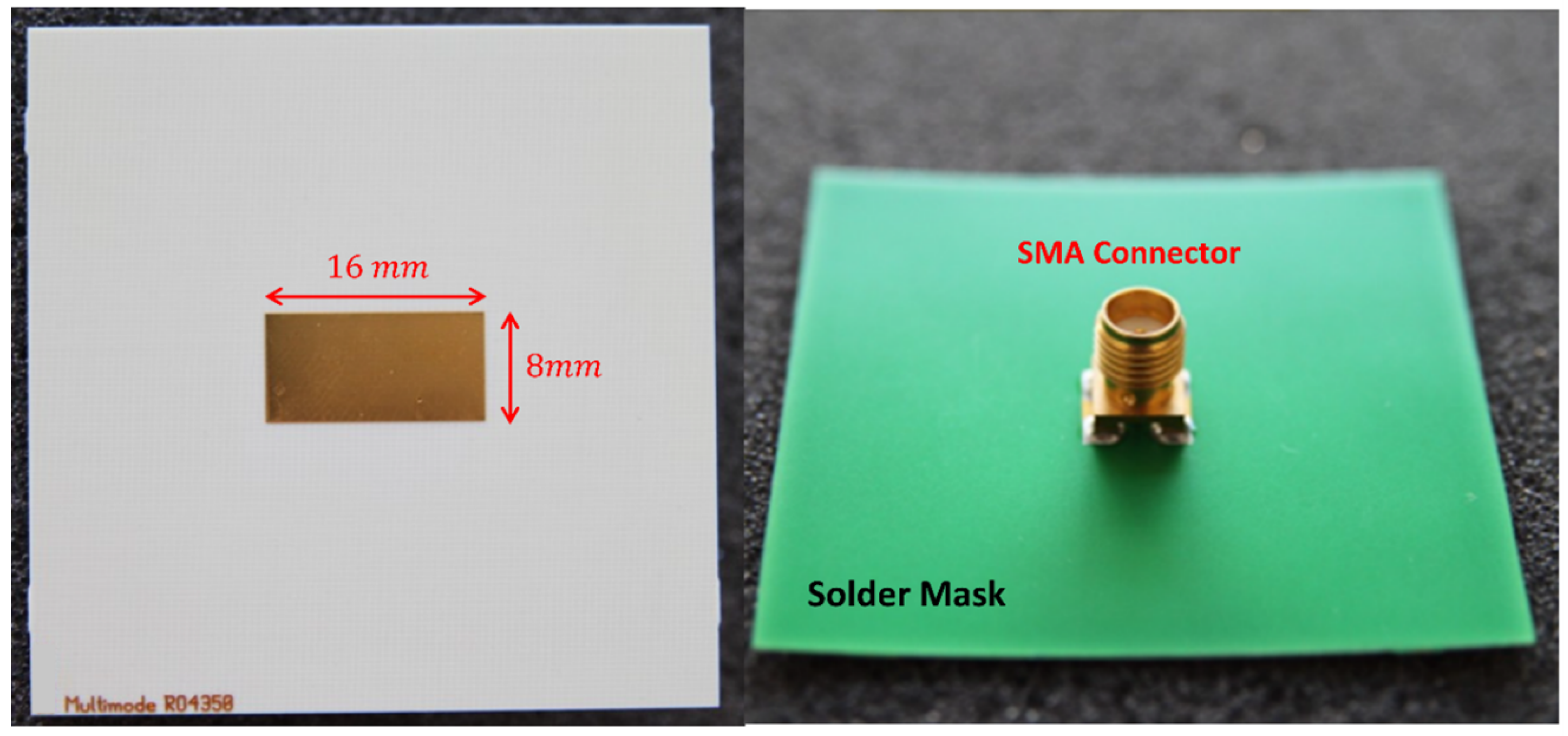
To visualize the impact of these variations, the antenna simulation model was built in CST Microwave Studio using the FIT solver. The substrate selected was RO4003C with a thickness of 0.2 mm, and the patch was excited using a vertical probe-feed through an SMA connector. Boundary conditions were set to open (add space), and a mesh size of
was used for all structures. Simulation calibration was extended to 20 GHz to ensure accurate wideband behavior. These settings were selected to match the physical measurement setup as closely as possible. The antenna was fabricated on a 0.2 mm-thick RO4003C dielectric substrate.
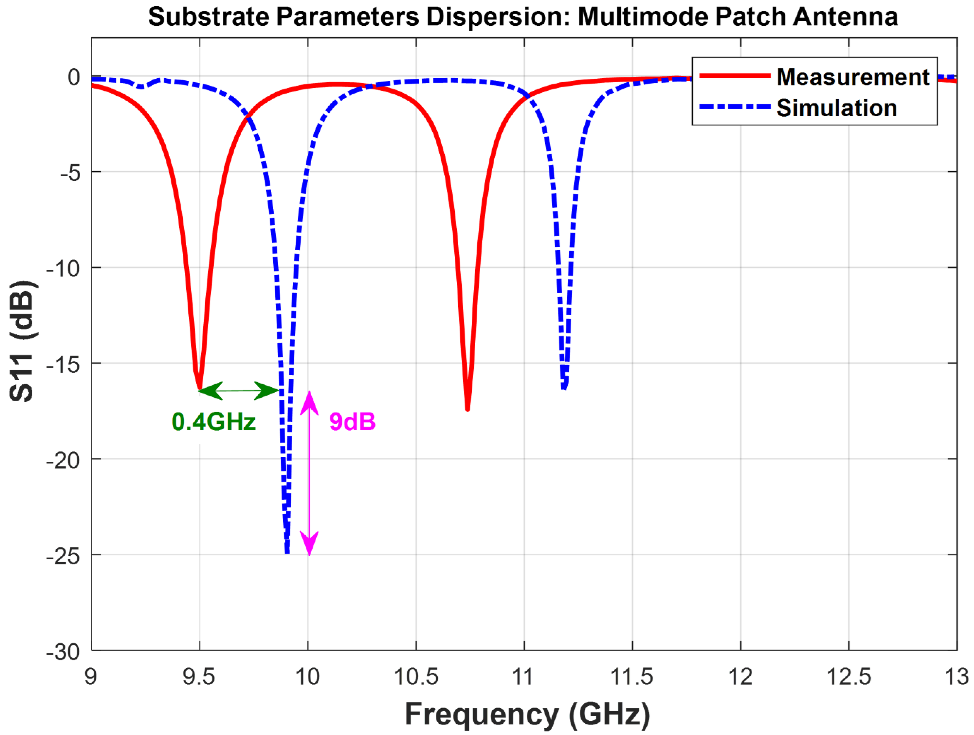
Figure 2 visually represents the simulation (dotted line) alongside the experimental results, following
measurements. In particular, a slight dispersion in
resulted in a resonant frequency shift of approximately 400 MHz in the lower mode. Additionally, a minor
dispersion contributed to an approximate 9 dB difference in the
minimum. These shifts underscore the critical role of substrate characterization in ensuring reliable antenna design.
These discrepancies are attributed to the influence of high fringing fields and the roughness of the material’s surface. Such effects can manifest in various distributed device structures such as antennas, filters, and couplers. Given the low substrate height, the modification of the field lines by surface roughness induces an increase in capacitance between the designed antenna and the ground plane. This higher capacitance significantly increases the relative permittivity value, highlighting the need for a high relative permittivity value to align with the results observed in
Figure 2.
2.2. Step 2: Tuning of Substrate Parameters
To ensure precise alignment between the EM simulations and the experimental results, the substrate parameters
and
were numerically tuned. According to Equation (
1), when the physical dimensions (L, W, h) of the fabricated multimode antenna perfectly match the simulation settings, variations in the resonant frequencies (
) are mainly influenced by the relative permittivity
. However, as indicated by Equation (
1), the resonant frequencies
are sensitive to changes in both the physical dimensions (i.e.,
) and the relative permittivity, each of which can induce shifts in frequencies. Therefore, it is crucial to measure effective antenna dimensions, including the top conductor geometry and substrate thickness, and incorporate these measurements into the CST V20 EM software settings before proceeding with data fitting. In this work, antenna dimensions were initially measured using a microscope to achieve the accuracy required to estimate the physical dimensions. Additionally, to maintain measurement precision, the substrate thickness for both multimode and monomode antennas was controlled within
of the nominal value during fabrication. Although thickness variations can shift resonant frequencies and alter input impedance, the iterative tuning algorithm effectively compensates for such deviations by adjusting
and
to match measured data.
The fitting procedure was enhanced through a series of validation steps, ensuring that the input impedance remained consistent with the expected values throughout the tuning process. Performing complete curve fitting across a broad spectrum of frequencies, such as from 8 to 16 GHz, is computationally demanding due to the time-consuming nature of EM-simulation software. This method is not well-suited for use with the measured data in this work. Instead, a more efficient approach was employed. The fitting process focused on two key parameters: the resonant frequencies of all modes and segments of the curve within 500 MHz around . In particular, the decision to fit only the peak value would not provide a comprehensive representation of the matching quality by itself. Hence, the chosen approach, targeting resonant frequencies and specific portions of the curve, ensures a more nuanced and accurate assessment of the matching quality without the computational burden associated with complete curve fitting.
The tuning process was executed to ensure precision in the characterization of the substrate parameters. Initially, the resonant frequency was tuned by adjusting until the relative error between simulation and measurement fell below 0.2%. The impact of on the values was temporarily ignored during this phase.
Once the optimal value of had been determined—ensuring accurate alignment of the resonant frequencies—the fitting procedure progressed to tuning the loss tangent . This step focused on matching the amplitude characteristics of the simulated and measured curves in the vicinity of each resonance . Rather than influencing the resonant frequency position, was iteratively adjusted to reproduce the depth of the null and the corresponding amplitude of the input impedance , capturing the energy-dissipation effects inherent to dielectric losses. This process of sequential adjustment helps in isolating the effects of each parameter, enabling a more precise tuning strategy. This iterative process continued with a reasonable number of steps and simulation time. The partial curve-fitting ceased when the mean relative error (MRE) on the target points dropped below 10%, ensuring a correlation exceeding 90%.
Notably, ’s influence on is minimal, a factor that facilitates a progressive convergence of the tuning procedure and ensures reliable identification of the solution.Achieving MRE < 5% can be made feasible by extending the number of tuning steps, depending on the accuracy requirements of the specific application. For this work, a 90% correlation between simulation and measurement data of on MHz around was deemed sufficiently accurate, providing a robust foundation for substrate parameter characterization.
In optimizing parameter tuning, a linear fixed step, while straightforward, proved impractical for this work. The extensive time required by the EM time-domain solver to traverse all predefined sweeping values, especially when the target value deviates significantly from the manufacturer’s data, rendered this method unsuitable. Furthermore, the use of Newton’s method for root-finding faced limitations due to the intricate mathematical relations linking to and to within the complex EM simulator.
A more effective approach emerged with the utilization of the secant iterative algorithm. Its application in this work was facilitated by the monotonic behavior exhibited by the functions described in Equation (
1). The secant iterative algorithm provides a practical and efficient means of achieving accurate parameter tuning, overcoming the limitations of direct sweeping and Newton’s method.
The tuning algorithm outlined in Equations (
2)–(
5) forms a crucial part of this methodology, ensuring precise parameter adjustments for optimal antenna performance. Equation (
2) governs the iterative tuning of relative permittivity to match the measured resonant frequency:
is the measured resonant frequency of the experimental results, and
is the relative permittivity at step k. The iterative process is repeated until 99.8% accuracy is reached (0.2% relative error) per Equation (
3):
Equation (
4) defines the iterative tuning of the loss tangent (
) for accurate
curve fitting:
MRE (
) represents the mean relative error between measured and simulated values of
at iteration step
k. The constant value of 5 in Equation (
4) represents the ideal reference MRE for optimal loss-tangent tuning. This value is determined based on empirical analysis, ensuring that simulated and measured
values exhibit minimal deviation. The iterative process continues until the MRE value drops below 10%, as enforced by Equation (
5):
Here, N is the number of points in a bandwidth of ±500 MHz around , and and are the linear value of measured and simulated respectively.
Before the final step of the characterization process begins, a comparison is made between measured and simulated curves of the real and imaginary parts of the input impedance (). The target value for Real() is set at 50 to align with the SMA connector used for antenna feeding. A successful fitting ensures that Real() approaches 50 when Imag() is near 0 .
A summary of the implemented secant algorithm for parameter tuning is illustrated in
Figure 3.
2.3. Step 3: Validation by Monomode Antenna
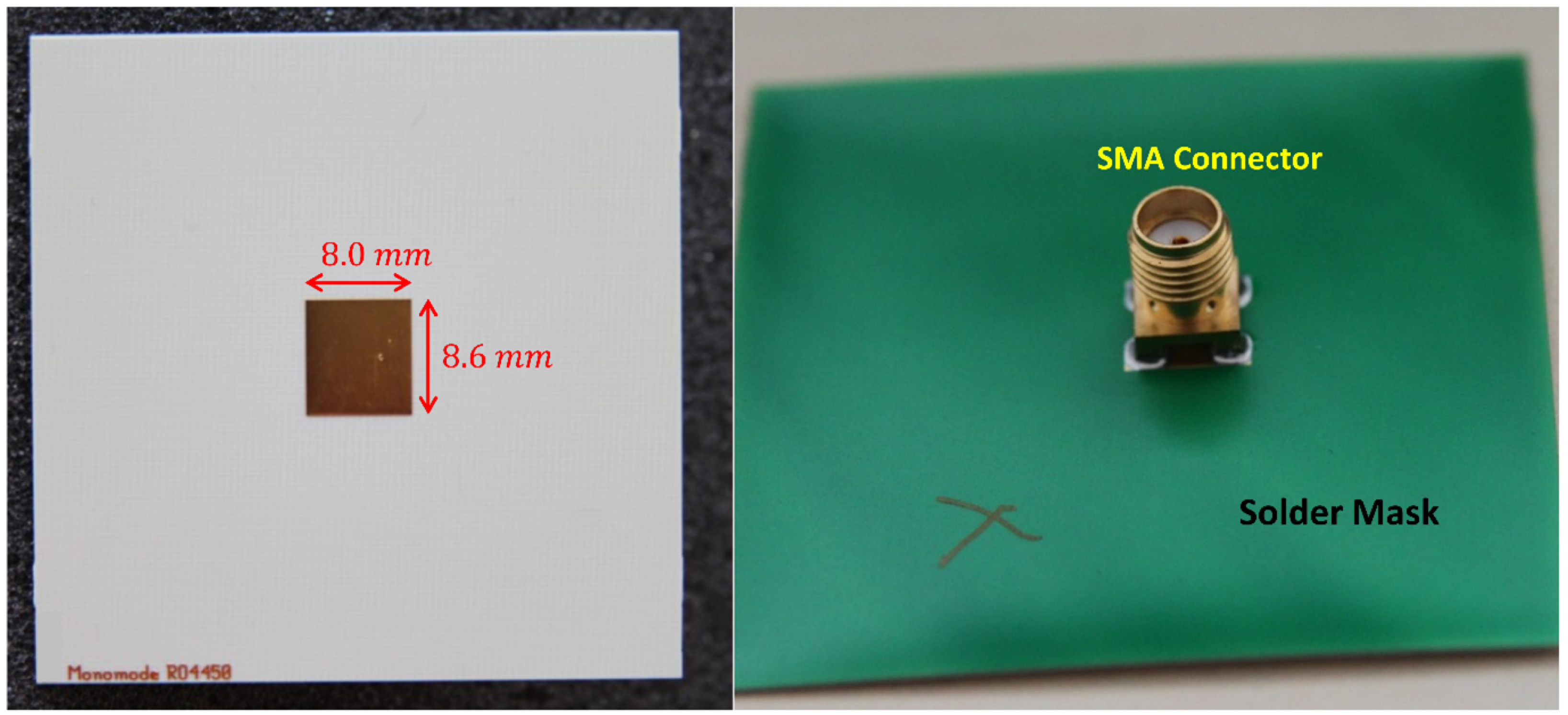
In the final phase, which is dedicated to validating the characterization method, a monomode rectangular patch antenna is designed on a new center frequency (around 8.6 GHz). The critical aspect of this step involves employing the tuned values of relative permittivity and loss tangent obtained from Step 2. Subsequently, the designed monomode antenna undergoes the stages of fabrication, measurement, and a comparison with the design simulations for thorough verification. This phase serves as a critical test of the entire characterization process, ensuring that the parameters obtained from the multimode fitting accurately predict the performance of a simpler single-resonance system.
To enhance the robustness of the validation phase, measurements of the monomode antenna were compared to values obtained from simulations conducted on two distinct high-performance 3D EM-analysis software (CST V20) platforms. These software solutions employed diverse solving methods, including the time-domain Finite-Integration-Technique (FIT, akin to FDTD) in CST Microwave Studio and the frequency-domain Finite Element Method (FEM) in Keysight ADS. This dual-software comparison ensured a comprehensive assessment of the monomode antenna’s performance, affirming the reliability and accuracy of the proposed characterization method across different simulation platforms and methodologies.
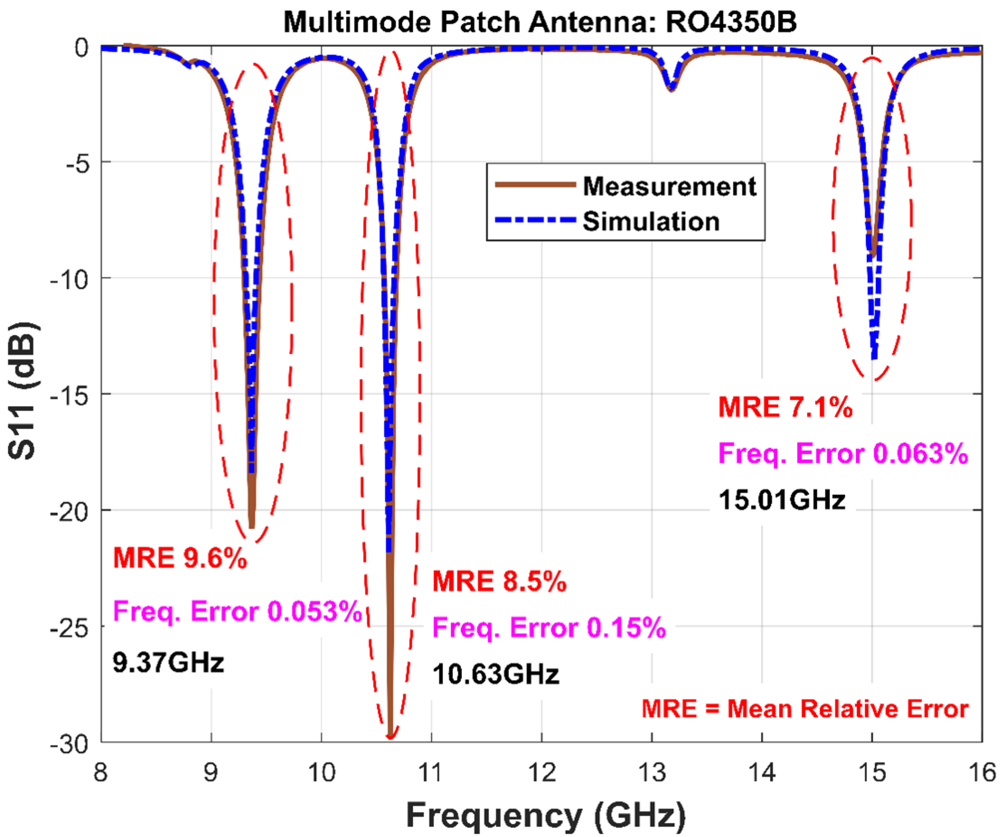
To ensure the accuracy of the validation phase, the resonant frequency shift and partial curve-fitting accuracy are estimated. These estimates are then compared with the identical target criteria utilized in Step 2, which requires a relative error below 0.2% on and an MRE < 10% on the curve. To further enhance the verification process, an additional check is performed on the quality factor of impedance matching in the measured and simulated curves of the monomode antenna.
For validation to be considered valid, the method stipulates that the bandwidth over which must exhibit a relative error of 10%. This corresponds to a matching error of 10 MHz on a bandwidth of 100 MHz. serves as one of the indicators of the quality of antenna matching.
A key benefit of the proposed method is its natural wideband characteristics. Multimode antennas inherently cover a broad spectrum of frequencies, ensuring that the characterization results remain valid across a wide range of operating microwave frequencies. This broadens the applicability and reliability of the method for diverse microwave-frequency scenarios.
4. Strengths and Limitations of the Proposed Methodology
One of the primary strengths of the proposed methodology is its wideband capability, as it effectively spans the 8–16 GHz frequency range. This enables a comprehensive characterization of dielectric substrates across multiple frequencies, enhancing the applicability of the method in various sectors, including radar systems, telecommunications, and advanced material analysis. Compared to narrowband methods, the wideband approach captures frequency-dependent variations in material properties more effectively, providing more reliable insights for practical applications.
Another advantage of the presented technique lies in its iterative and retrospective simulation approach. This method continuously refines electromagnetic (EM) simulation models based on preliminary measurement results, significantly enhancing accuracy in predicting antenna performance. This iterative strategy streamlines the design process, shortens development timelines, and offers considerable benefits in industries that require rapid prototyping and validation.
Additionally, the extracted parameters reflect effective dielectric behavior under realistic circuit conditions, capturing the influence of fringing fields, conductor surface roughness, SMA transitions, and surface wave propagation. While these values may not align exactly with metrological standards derived from idealized laboratory settings, they offer improved predictive accuracy in EM simulations. This makes the method highly relevant for design engineers seeking alignment between simulation and measurement, particularly for those working with modified, aged, or non-standard substrates.
However, the methodology does have certain limitations. Primarily, it currently relies on destructive testing methods, which may not be suitable for applications requiring non-destructive evaluation.
5. Conclusions and Future Work
In this work, we present a systematic and cost-effective methodology for the accurately characterization of dielectric substrate materials using rectangle-shaped patch antennas. The process integrates a wideband antenna design, precise fabrication, full-wave electromagnetic simulation, and iterative parameter fitting to extract both relative permittivity () and loss tangent () values over the 8–16 GHz band. Validation was performed using monomode antennas to cross-check the extracted parameters, thereby reinforcing the robustness of the approach.
While patch antennas have been historically employed in substrate characterization [
14], our work significantly refines this principle by introducing a wideband, multimode-based extraction process that accounts for practical fabrication variabilities and electromagnetic nonidealities. This refinement is particularly beneficial for low-height substrates (≤0.4 mm), for which traditional resonator-based methods often overlook critical effects such as fringing fields, surface wave propagation, and conductor losses.
We validated the methodology on three commercial low-height substrates using both time-domain (CST/FIT) and frequency-domain (ADS/FEM) solvers. The results show excellent agreement between simulation and measurement, with mean relative errors below 10% in the curves and resonant-frequency deviations under 0.2%. These outcomes demonstrate the accuracy, scalability, and reproducibility of our workflow across different platforms and material types.
This work contributes a practical advancement rather than a conceptual novelty. It provides a reproducible and transferable method for RF engineers and researchers seeking to characterize low-height-film materials beyond datasheet approximations—especially in design scenarios involving emerging packaging technologies, compact multilayer circuits, and high-frequency-signal integrity.
Future extensions of this method may include variants using non-destructive characterization, applications involving broader frequency ranges, and testing on novel substrate families such as flexible dielectrics and advanced composites. Such developments could enable critical support for next-generation technologies, including 5G/6G communication systems, wearable electronics, and conformal antennas.

